What occurs when PCB power integrity fails in high-speed circuit designs? Poor power integrity leads to signal distortion, component malfunction and shortened product lifespan, making it a critical aspect of high-speed PCB design. This guide details everything needed to understand, analyze, simulate and optimize PCB power integrity for high-performance, reliable electronic devices.
What is PCB Power Integrity in High-Speed Circuit Design?
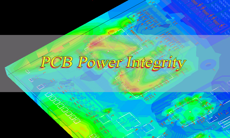
PCB power integrity refers to the ability of a PCB’s power distribution network to deliver clean, stable power to all components at required voltage and current levels. In high-speed circuit designs where signal frequencies exceed 1 GHz and components demand rapid current changes, maintaining consistent power delivery becomes significantly more challenging.
Unlike low-speed designs, high-speed circuits are highly sensitive to voltage fluctuations and noise. Even minor deviations from ideal voltage can cause timing errors, signal degradation and functional failures. PCB power integrity ensures the power distribution network minimizes noise, voltage drop and impedance variations to provide a reliable power supply to every active component on the board.
The core goal of PCB power integrity is maintaining stable voltage across all component power pins even as current demands change rapidly. This requires careful design of the power distribution network including power planes, vias, traces and decoupling components to minimize parasitic inductance and capacitance that contribute to power-related problems.
Why Does PCB Power Integrity Matter for High-Speed PCB Performance and Reliability?
PCB power integrity directly impacts the performance and reliability of high-speed PCBs. Without proper power integrity, even well-designed signal paths fail to deliver expected performance resulting in costly rework, delays and product failures. Below are the key reasons it matters.
- Prevents Signal Distortion: Power noise and voltage fluctuations couple into signal traces causing jitter, skew and signal degradation. This is especially critical in high-speed interfaces like DDR5, PCIe and Ethernet where even small signal distortions lead to data errors.
- Ensures Component Longevity: Consistent voltage delivery prevents overheating and stress on components. Voltage spikes or drops damage sensitive ICs reducing their lifespan and increasing failure rates in field applications.
- Meets Regulatory Requirements: Many industries require electronic devices to meet strict electromagnetic compatibility standards. Poor PCB power integrity increases electromagnetic interference emissions making it difficult to pass compliance tests.
- Reduces Design Iterations: Addressing PCB power integrity early in the design process avoids costly rework and redesigns. Fixing power-related issues after prototyping or manufacturing adds significant time and expense to a project.
- Supports High-Density Designs: Modern high-speed PCBs feature smaller components and tighter spacing. Proper power integrity ensures these dense designs operate reliably without crosstalk or power-related failures.
How Does PCB Power Integrity Differ from PCB Signal Integrity?
PCB power integrity and PCB signal integrity are closely related but address distinct aspects of high-speed PCB design. Both are critical for performance but focus on different parts of the circuit and solve different problems. The table below highlights their key differences.
| Comparison Dimension | PCB Power Integrity | PCB Signal Integrity |
| Function | Deliver clean, stable power to all components via the power distribution network, ensuring consistent voltage and current under dynamic load conditions. | Ensure signals transmit from source to load with minimal distortion, maintaining signal fidelity and timing accuracy across high-frequency operations. |
| Challenges | Voltage drop, power noise, power plane impedance mismatches, inadequate decoupling, via parasitics, and power plane resonance. | Signal reflections, crosstalk, jitter, insertion/return loss, timing skew, and electromagnetic interference coupling. |
| Components Involved | Power regulators, decoupling capacitors, power/ground planes, power vias, and current-carrying connectors. | Signal traces, transmission lines, IC I/O pins, signal connectors, and termination components. |
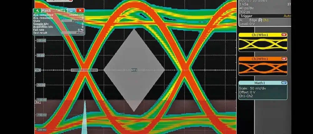
| Measurement Indicators | Voltage ripple amplitude, power plane impedance, voltage drop percentage, and noise spectral density. | Eye diagram parameters, jitter magnitude, insertion/return loss values, and crosstalk coupling level. |
| Design Optimization Strategies | Power plane optimization, strategic decoupling capacitor placement, via parasitic minimization, and impedance matching for power paths. | Controlled impedance routing, trace length matching, shielding, proper termination, and crosstalk mitigation. |
What are the Common Issues Affecting Power Integrity in PCB Design?
Power integrity in PCB designs faces several common challenges especially in high-speed and high-density applications. These issues often stem from poor power distribution network design, component selection or layout practices. Understanding these issues is the first step to resolving them.
- Voltage Drop: Occurs when current flows through power traces, vias or planes creating a reduction in voltage at the component. High current demands in high-speed ICs exacerbate this issue leading to voltage levels below the component’s operating range. Target voltage drop should not exceed 3% for most applications.
- Power Noise: Includes voltage ripple, switching noise and electromagnetic interference. Switching noise from digital components creates voltage fluctuations in the power distribution network that couple into signal traces and cause distortion. Common sources include clock signals, data buses and power regulators.
- Impedance Mismatches: Power planes and traces have inherent impedance. Mismatches between the power source, distribution network and load cause reflections increasing noise and voltage fluctuations. For example, DDR5 power planes require impedance of 3mΩ or less to maintain stability.
- Poor Decoupling: Decoupling capacitors filter out high-frequency noise and provide instant current to components. Issues include using the wrong capacitor values, placing capacitors too far from component pins or using capacitors with high parasitic inductance. This leads to inadequate noise suppression and voltage instability.
- Power Plane Resonance: Power and ground planes form a resonant cavity. At specific frequencies this cavity resonates amplifying noise and increasing impedance. Resonance is often caused by improper plane size, shape or spacing between power and ground planes.
- Via Parasitics: Vias used to connect power planes across layers introduce parasitic inductance and capacitance. Excessive via inductance slows current delivery and increases noise especially in high-speed designs where current changes rapidly. Prioritize vias with 0.3mm or larger apertures to minimize parasitic inductance.
How to Perform Effective Power Integrity Analysis in PCB?
Effective power integrity analysis identifies potential issues early in the design process reducing the risk of failures and rework. The process combines design reviews, simulation and measurement to evaluate the power distribution network’s performance. Below are the key steps to perform thorough analysis.
- Review Power Distribution Network Design: Start with a detailed review of the power distribution network layout. Check power plane size, trace width, via placement and component spacing. Ensure power planes are adjacent to ground planes to minimize impedance and noise.
- Calculate Target Impedance: Determine the required impedance for the power distribution network based on component specifications. Use impedance formulas to verify that power planes, traces and vias meet the target. For example, CPU 12V power planes typically require impedance of 5mΩ or less.
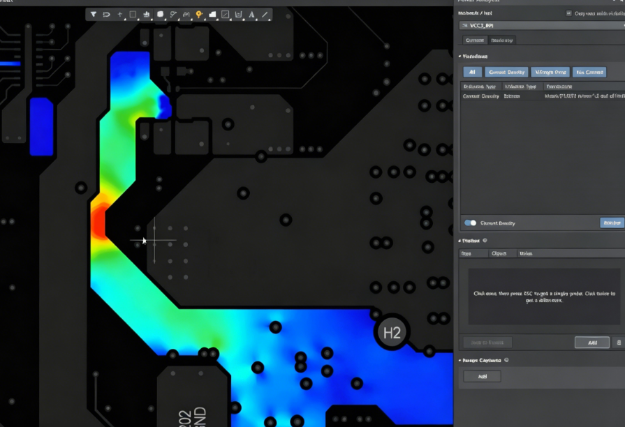
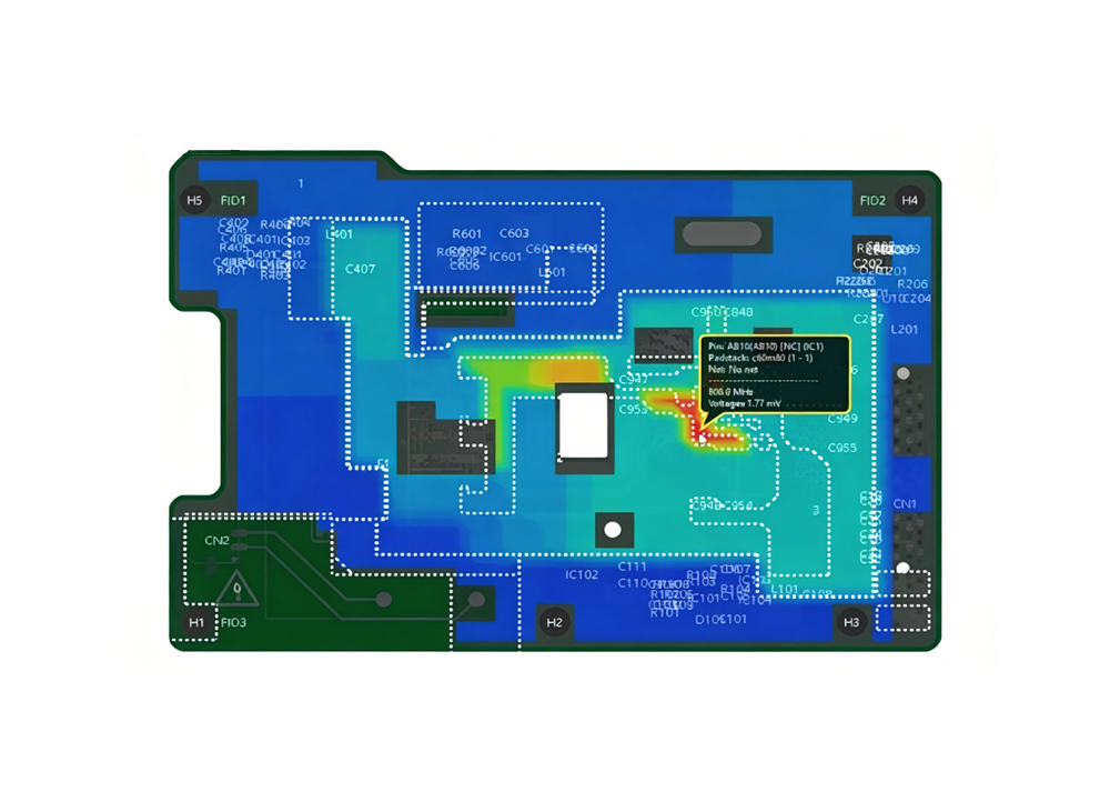
- Simulate Power Delivery: Use specialized simulation tools to model the power distribution network. Simulate voltage drop, noise and impedance across different frequencies to identify problem areas. Focus on high-current components and high-frequency operation.
- Analyze Decoupling Effectiveness: Evaluate the placement and selection of decoupling capacitors. Simulate their performance to ensure they filter noise effectively and provide adequate transient current. Test different capacitor combinations to optimize noise suppression.
- Measure Prototype Performance: After prototyping use test equipment like oscilloscopes and network analyzers to measure actual voltage drop, noise and impedance. Compare results with simulation data to validate the design and identify any discrepancies.
- Iterate and Optimize: Use analysis results to make design adjustments. Modify power plane layout, adjust decoupling capacitor placement or change component values to resolve identified issues. Repeat the analysis process until the power distribution network meets all requirements.
What Tools Are Essential for PCB Power Integrity Simulation and Analysis?
PCB power integrity simulation and analysis require specialized tools to model complex power distribution networks, simulate performance and measure real-world behavior. The right tools help identify issues early and optimize designs efficiently. Below are the essential tools for the process.
- Power Distribution Network Simulation Tools: These tools model the power distribution network to simulate voltage drop, noise and impedance. They use circuit solvers and electromagnetic solvers to accurately predict performance. Examples include tools with mixed simulation engines that handle complex plane structures and parasitic parameters.
- Electromagnetic Simulation Tools: Used to analyze electromagnetic interference and power plane resonance. These tools simulate the interaction between power planes, traces and components identifying resonance points and noise sources. They are critical for high-speed designs where electromagnetic effects are significant.
- Oscilloscopes: Essential for measuring real-world voltage ripple, noise and voltage drop on prototypes. High-bandwidth oscilloscopes (1 GHz or higher) capture fast transient signals allowing accurate measurement of power-related noise. Probe selection is critical; use low-inductance probes for precise measurements.
- Network Analyzers: Measure the impedance of the power distribution network across a range of frequencies. This helps identify resonance points and impedance mismatches that contribute to power integrity issues. Network analyzers are also used to validate simulation results against physical measurements.
- PCB Design Software with PI Analysis: Integrated PCB design tools with built-in power integrity analysis features allow designers to check power distribution network performance during layout. These tools flag issues like inadequate trace width, poor via placement or insufficient decoupling enabling real-time optimization.
- SPICE Simulators: Used to model the power distribution network at the component level. SPICE simulators analyze the behavior of power regulators, capacitors and other components helping optimize the power delivery path. They are particularly useful for evaluating decoupling capacitor performance.
What Steps Are Involved in PCB Power Integrity Simulation for High-Speed Boards?
PCB power integrity simulation for high-speed boards follows a structured process to ensure accurate results and actionable insights. The process involves setting up the model, defining parameters, running simulations and analyzing results. Below are the key steps to follow.
1. Define Simulation Objectives: Clearly outline what you want to achieve with the simulation. Common objectives include measuring voltage drop, identifying noise sources, verifying decoupling effectiveness or locating power plane resonance. Define acceptance criteria for each objective to evaluate results.
2. Create the Power Distribution Network Model: Build a detailed model of the power distribution network using simulation software. Include power planes, traces, vias, power regulators, decoupling capacitors and load components. Use accurate component models including parasitic parameters like ESR and ESL for capacitors.
3. Set Up Simulation Parameters: Define the simulation parameters including frequency range, input voltage, load current and operating conditions. For high-speed boards simulate frequencies up to 10 GHz to capture high-frequency noise and resonance. Set up transient simulations to model rapid current changes.
4. Run the Simulation: Execute the simulation based on the defined parameters. Run multiple simulations if needed such as frequency-domain simulations for impedance and noise and time-domain simulations for voltage drop and transient response. Ensure the simulation converges to accurate results.
5. Analyze Simulation Results: Review the simulation data to identify issues. Check voltage drop across critical components, noise amplitude, impedance levels and resonance points. Compare results against acceptance criteria to determine if the power distribution network meets requirements.
6. Optimize the Design: Make design adjustments based on simulation results. Modify power plane layout, adjust decoupling capacitor placement or values or change trace widths to resolve issues. Re-run the simulation to verify that changes improve power integrity.
7. Validate with Physical Measurements: After optimizing the design prototype the PCB and measure real-world performance using oscilloscopes and network analyzers. Compare measurement results with simulation data to confirm accuracy and ensure the design meets all requirements.
How to Optimize Power Integrity in PCB Design to Reduce Noise and Voltage Drop?
Optimizing power integrity in PCB design reduces noise and voltage drop ensuring stable power delivery to components. The process involves design choices that minimize impedance, suppress noise and improve current delivery. Below are practical optimization techniques.
- Optimize Power Plane Design: Use large, solid power planes to minimize impedance. Place power planes adjacent to ground planes with a small layer spacing (0.2mm or less) to maximize parallel plate capacitance reducing impedance. Ensure power planes are complete with minimal splits and use isolation bands for different voltage domains.
- Select and Place Decoupling Capacitors Strategically: Use a combination of high-frequency and low-frequency capacitors to filter noise across a wide frequency range. Place high-frequency capacitors (0.1μF MLCC, X7R material) within 1mm of component power pins and low-frequency capacitors (10μF MLCC + 100μF aluminum electrolytic) nearby. Use short, wide traces for capacitor connections to minimize parasitic inductance.
- Minimize Via Parasitics: Use short, wide vias for power connections. Avoid using multiple vias in series and place vias close to component pins. For high-current applications use multiple vias to distribute current and reduce inductance. Use blind or buried vias to minimize trace length and parasitic effects.
- Control Trace Width and Length: Use wide enough traces to handle the required current and minimize resistance. For high-current paths increase trace width to reduce voltage drop. Keep power traces as short as possible to minimize inductance and noise. Avoid sharp bends in traces which increase impedance.
- Implement Impedance Control: Design power planes and traces to meet the target impedance. Use impedance calculation tools to determine the correct trace width, spacing and layer stackup. For high-speed designs ensure power plane impedance is consistent across the entire board.
- Reduce Switching Noise: Minimize the number of components switching simultaneously to reduce current spikes. Use power regulators with fast response times to handle transient current demands. Add ferrite beads or inductors to filter switching noise from power regulators.
What are the Considerations for Power Integrity in High-Density PCB Layouts?
High-density PCB layouts present unique challenges for power integrity including limited space, increased component density and tighter trace spacing. These factors can lead to higher impedance, increased noise and voltage drop. Below are key considerations to maintain power integrity in dense designs.
- Layer Stackup Design: Prioritize power and ground plane placement in the layer stackup. Use a symmetric stackup with power planes adjacent to ground planes to minimize impedance and noise. Allocate sufficient layer space for power distribution even in dense layouts.
- Component Placement: Group components by power domain to minimize power trace length. Place high-current components close to the power source to reduce voltage drop. Keep decoupling capacitors as close to component power pins as possible even in tight spaces.
- Trace Routing: Use microvias and blind/buried vias to route power traces in inner layers freeing up surface space. Avoid routing power traces through congested areas which can increase crosstalk and impedance. Use wide enough traces to handle current demands without excessive voltage drop.
- Decoupling Optimization: Use smaller decoupling capacitors (0402 or 0201 packages) to save space in dense layouts. Place capacitors in arrays around high-speed components to ensure each power pin has adequate decoupling. Use simulation to verify that decoupling is effective despite space constraints.
- Thermal Management: High component density increases heat which can degrade power integrity. Use thermal vias to dissipate heat from power components and power planes. Select components with lower power dissipation to reduce heat buildup which can affect voltage stability.
- Impedance Control: Maintain consistent impedance in power planes and traces even in dense layouts. Use impedance simulation to identify areas where spacing or trace width changes cause impedance mismatches. Adjust the layout to correct these issues without sacrificing space.
How Can You Identify and Resolve Power Integrity Issues in PCB Before Manufacturing?
Identifying and resolving power integrity issues before manufacturing saves time, money and rework. The process involves proactive analysis, simulation and design reviews to catch issues early. Below are steps to identify and resolve issues pre-manufacturing.
- Conduct Early Power Distribution Network Reviews: Review the power distribution network design during the schematic phase. Check component selection, power source sizing and decoupling strategy. Identify potential issues like inadequate trace width or improper component placement early.
- Use Pre-Layout Simulation: Run pre-layout simulations to model the power distribution network before finalizing the layout. Simulate voltage drop, noise and impedance to identify issues like insufficient decoupling or impedance mismatches. Adjust the design based on simulation results.
- Perform Layout Checks: Use PCB design software to run layout checks for power integrity. Check for trace width violations, via placement issues, power plane splits and decoupling capacitor placement. Fix any issues before proceeding to manufacturing.
- Run Post-Layout Simulation: After completing the layout run post-layout simulations to validate performance. Use detailed models of the actual layout including parasitic parameters to simulate real-world behavior. Compare results against design requirements.
- Validate with Design Rule Checks: Use design rule checks to ensure the layout meets power integrity requirements. Set rules for trace width, spacing, via placement and power plane design. Fix any rule violations that could impact power integrity.
- Consult Design Guidelines: Refer to component datasheets and manufacturer design guidelines for power integrity best practices. Many IC manufacturers provide specific recommendations for decoupling, power plane design and layout to ensure optimal performance.
How to Ensure Long-Term Power Integrity Performance in High-Speed PCB Applications?
Long-term power integrity performance is critical for the reliability of high-speed PCB applications especially in harsh environments or long-service-life products. Ensuring consistent performance over time requires careful design, component selection and testing. Below are key steps to achieve this.
- Select High-Quality Components: Choose components with stable electrical characteristics over time. Select decoupling capacitors with low ESR and ESL and power regulators with high stability and long lifespan. Avoid low-quality components that degrade over time leading to power integrity issues.
- Design for Thermal Stability: Heat is a major factor in component degradation. Design the PCB with adequate thermal management including thermal vias, heat sinks and proper airflow. Ensure power components operate within their temperature limits to maintain stable performance.
- Account for Aging Effects: Components like capacitors degrade over time affecting their decoupling effectiveness. Overdesign the decoupling network to account for aging ensuring adequate noise suppression even as components age. Use simulation to model aging effects and validate long-term performance.
- Test for Long-Term Reliability: Conduct accelerated aging tests on prototypes to simulate long-term use—adopt 85℃/85%RH environmental conditions for 1000 hours. Test voltage drop, noise and impedance over time to ensure they remain within acceptable limits. Make design adjustments if aging affects performance.
- Implement Protective Measures: Add overvoltage, overcurrent and ESD protection to the power distribution network. These measures prevent damage to components from voltage spikes or electrostatic discharge which can degrade power integrity over time.
- Monitor Performance in Field Applications: For critical applications implement monitoring systems to track power integrity metrics in the field. Use sensors to measure voltage, noise and temperature and use this data to identify potential issues before they cause failures.
How to Choose Professional Power Integrity Analysis Services in PCB?
Professional power integrity analysis services provide expertise and tools to optimize PCB designs especially for complex high-speed applications. Choosing the right service ensures accurate analysis and actionable recommendations. Below are key factors to consider when selecting a service.
- Expertise in High-Speed PCB Design: Select a service with experience in high-speed PCB design and power integrity. Look for services that specialize in your industry or application as they will understand the unique challenges and requirements.
- Advanced Simulation Tools: Ensure the service uses state-of-the-art simulation tools capable of modeling complex power distribution networks. Tools with mixed circuit and electromagnetic solvers provide the most accurate results for high-speed designs.
- Proven Track Record: Review the service’s past projects and client testimonials. Look for examples of successful power integrity optimization and design improvements. A proven track record indicates reliability and expertise.
- Comprehensive Analysis Capabilities: Choose a service that offers end-to-end power integrity analysis including pre-layout simulation, post-layout simulation, prototype testing and optimization. Comprehensive services provide a complete solution for power integrity issues.
- Timely Delivery: Ensure the service can deliver results within your project timeline. Delays in analysis can hold up design iterations and manufacturing increasing costs. Look for services with efficient processes and clear timelines.
- Cost-Effectiveness: Compare pricing across different services but prioritize value over cost. A high-quality service may cost more upfront but can save money by reducing rework and failures. Look for transparent pricing with no hidden fees.
- Technical Support: Choose a service that provides ongoing technical support. This includes answering questions, explaining results and assisting with design optimization. Good support ensures you can implement the service’s recommendations effectively.
FAQs About High-Speed PCB Power Integrity Analysis & Simulation
Q1: What is the acceptable voltage drop for power integrity in high-speed PCB designs?
A1: The acceptable voltage drop for most high-speed PCB designs is 3% or less of the nominal voltage. For critical components like CPUs and DDR memory the voltage drop should be kept below 2% to ensure stable performance. Exceeding these limits can cause timing errors and component failure.
Q2: How do decoupling capacitors improve power integrity in PCB designs?
A2: Decoupling capacitors improve power integrity by filtering high-frequency noise and providing instant transient current to components. They act as local power reservoirs reducing voltage fluctuations caused by rapid current changes. Properly placed capacitors minimize impedance in the power distribution network suppressing noise and voltage drop.
Q3: Can power integrity issues cause signal integrity problems in high-speed PCBs?
A3: Yes, power integrity issues frequently cause signal integrity problems. Power noise and voltage fluctuations couple into signal traces leading to jitter, skew and signal distortion. This is especially common in high-speed interfaces where even small signal changes can cause data errors. Resolving power integrity issues often improves signal integrity.
Q4: What is the difference between pre-layout and post-layout power integrity simulation?
A4: Pre-layout simulation is done before the PCB layout is finalized using simplified models of the power distribution network. It helps identify potential issues early in the design process. Post-layout simulation uses the actual layout geometry including parasitic parameters to provide accurate performance predictions. It validates the final design before manufacturing.
Q5: How can I reduce power plane resonance in high-speed PCB designs?
A5: To reduce power plane resonance optimize the size and shape of power and ground planes to avoid resonant frequencies within the operating range. Use decoupling capacitors to dampen resonance and reduce impedance at critical frequencies. Ensure power planes are adjacent to ground planes with minimal spacing to increase capacitance and reduce resonant effects.
Q6: What tools are best for measuring power integrity in PCB prototypes?
A6: The best tools for measuring power integrity in PCB prototypes are high-bandwidth oscilloscopes (1 GHz or higher) for measuring voltage ripple and noise and network analyzers for measuring power distribution network impedance. Low-inductance probes are essential for accurate oscilloscope measurements as they minimize parasitic effects.
Q7: How does PCB layer stackup affect power integrity?
A7: PCB layer stackup directly affects power integrity by influencing impedance, noise and heat dissipation. Placing power planes adjacent to ground planes minimizes impedance and noise. A symmetric stackup reduces warpage and improves signal and power integrity. Allocating sufficient layers for power distribution ensures stable current delivery in high-speed designs.