

When PCB heat dissipation fails, components can be damaged, and product lifespan shortened so how do you implement effective techniques to avoid this? PCB heat dissipation is vital for electronic design, as excess heat causes component failure, signal distortion, and safety risks. This guide explains everything needed to understand, design, and optimize heat dissipation in PCB, from basic concepts to advanced methods, ensuring stable, reliable, and cost-effective designs.
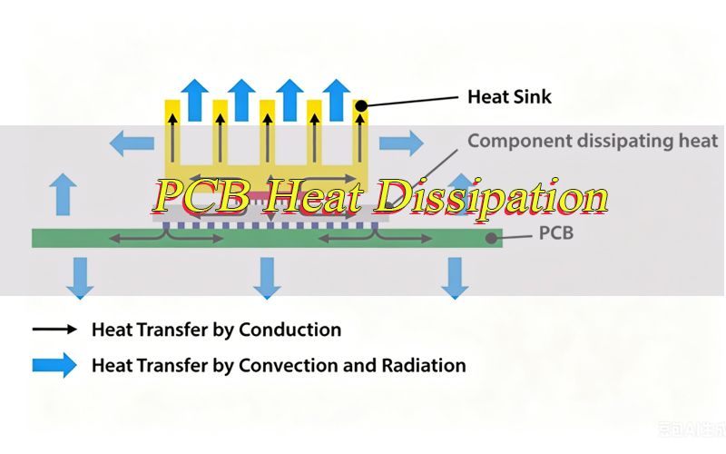
What is PCB Heat Dissipation and Why is it Critical?
PCB heat dissipation is the process of transferring heat from PCB-mounted electronic components to the surrounding environment to prevent localized overheating. PCBs act as both component platforms and heat transfer media, as all electronic components generate heat during operation.
Excessive heat buildup damages components: temperatures exceeding a component’s operating limit cause rapid performance degradation, permanent damage to capacitors and resistors, and premature product failure. In high-reliability applications (automotive electronics, industrial control systems), poor PCB heat dissipation leads to system downtime, safety hazards, and increased maintenance costs, even risking PCB substrate carbonization and fire in extreme cases.
PCB heat dissipation is critical for three core reasons: it extends component lifespan by keeping parts within rated temperature ranges, maintains consistent system performance and signal integrity, and minimizes fire or malfunction risks, especially in high-power or enclosed devices.
What Causes Excessive Heat in PCB Heat Dissipation?
Excessive heat in PCB heat dissipation comes from component, design, and environmental factors. Identifying these causes is the first step to effective solutions, as each issue needs targeted adjustments to restore proper heat transfer.
- High Power Density Components – Power transistors, voltage regulators, and LED drivers generate significant heat due to high power consumption. Dense packing of these components on a PCB leads to rapid heat accumulation, overwhelming natural heat dissipation.
- Poor Component Layout – Placing high-heat components too close together or in confined areas (such as PCB corners) creates hotspotslocalized extreme heat that degrades nearby components and disrupts overall heat dissipation in PCB.
- Inadequate Copper Pour – Copper is an excellent thermal conductor, but insufficient copper area or thin layers limit heat transfer. Small trace widths or gaps in copper pours prevent even heat spread across the PCB.
- Low-Quality Substrate Materials – Standard substrates like FR-4 have low thermal conductivity, making it hard for heat to transfer from components to the PCB surface. This creates bottlenecks in heat dissipation in PCB, especially for high-power designs.
- Enclosed or Poorly Ventilated Environments – PCBs in sealed enclosures or low-airflow areas cannot release heat to the environment. Stagnant air traps heat, causing steady temperature rises during operation.
- Thermal Resistance Issues – Poor solder joints, missing thermal interface materials, or gaps between components and heat sinks increase thermal resistance, slowing heat transfer and causing excessive heat buildup.
How to Calculate PCB Heat Dissipation Accurately for Your Project?
Accurate calculation of heat dissipation in PCB ensures designs meet thermal requirements without over engineering or waste. The process involves calculating total heat generation, thermal resistance, and expected temperature rise, using simple formulas and component specifications.
- Calculate Total Power Dissipation – Sum the power consumption of all PCB components. For each component, use the formula P = V × I (power = voltage × current) or refer to the datasheet for power dissipation values (often labeled Pmax or TDP).
- Determine Thermal Resistance – Thermal resistance (Rθ), measured in °C/W, indicates how well heat transfers through a material or assembly. Key values include RθJA (junction to ambient), RθJC (junction to case), and RθPCB (junction to PCB)all found in component datasheets.
- Calculate Temperature Rise – Use the formula ΔT = P × RθJA, where ΔT is temperature rise (°C), P is total power dissipation (W), and RθJA is total thermal resistance from component junction to ambient. This gives the component’s expected junction temperature relative to the environment.
- Verify Against Component Limits – Compare the calculated junction temperature (ambient temperature + ΔT) to the component’s maximum rated junction temperature (Tjmax) from the datasheet. If it exceeds Tjmax, adjust the design to improve heat dissipation in PCB.
- Use Thermal Simulation Tools – For complex designs, tools like ANSYS Icepak or Flotherm simulate heat distribution, identify hotspots, and validate calculations. These tools account for component layout, copper distribution, and airflow, delivering more accurate results than manual calculations.
Which PCB Substrate Materials Boost PCB Heat Dissipation?
PCB substrate material directly impacts heat dissipation in PCB, as different materials have varying thermal conductivity. Choosing the right substrate ensures efficient heat transfer from components to the PCB surface and environment, reducing hotspots and component stress.
- Aluminum-Based PCBs (MCPCB) – Aluminum (thermal conductivity 200–237 W/m·K) is ideal for high-heat applications like LEDs and power electronics. Aluminum-based PCBs transfer heat quickly to the aluminum base, which acts as a built-in heat sink. They are lightweight and cost-effective for medium-power designs.
- Copper-Based PCBs – Copper (385 W/m·K) has the highest thermal conductivity among common substrates. Used in high-power applications like industrial power supplies and automotive electronics, copper-based PCBs deliver maximum heat dissipationthey cost more than aluminum-based options but offer superior performance.
- High-Thermal FR-4 – Standard FR-4 (0.3–0.5 W/m·K) has low thermal conductivity, but high-thermal FR-4 (modified with ceramic fillers, 1.0–2.0 W/m·K) is a cost-effective alternative to metal-based substrates for low to medium-power designs. It remains compatible with standard PCB manufacturing processes.
- Ceramic Substrates – Ceramic materials like alumina (Al2O3) and aluminum nitride (AlN) have high thermal conductivity (150–300 W/m·K) and excellent electrical insulation. They are used in high-temperature, high-power applications like aerospace and military electronics, where extreme-reliability is required.
- Hybrid Substrates – Hybrid substrates combine materials (e.g., FR-4 with copper or aluminum inserts) to balance thermal performance and cost. They are ideal for designs with mixed high-heat and low-heat components, focusing heat dissipation on critical areas.
How to Dissipate Heat from PCB Effectively at Low Cost?
Effective heat dissipation in PCB does not require expensive components or complex designs. Several low-cost techniques significantly improve heat transfer, making them perfect for budget-constrained projects or low-power applications.
- Optimize Copper Pour – Increase copper pour area on power and ground planes. Copper is affordable and effective for thermal conduction; larger copper areas spread heat evenly across the PCB. Use 2oz copper instead of 1oz for critical areas to boost thermal conductivity without major cost increases.
- Improve Component Layout – Spread high-heat components to avoid hotspots. Place high-power components near PCB edges, where heat dissipates more easily to the environment. Keep heat-sensitive components (e.g., sensors, capacitors) away from hotspots to prevent performance degradation.
- Add Thermal Relief Pads – Thermal relief pads are small copper pads connected to larger copper areas via narrow traces. They transfer heat from components to the main copper pour while simplifying soldering. They are low-cost and require no additional components.
- Use Natural Convection – Design the PCB to leverage natural airflow. Mount it vertically to let hot air rise and cool air replace it. Avoid blocking airflow with components or enclosures, and leave gaps between PCBs in multi-board systems.
- Apply Thermal Interface Material (TIM) – Low-cost TIMs like thermal paste or adhesive pads fill gaps between components and heat sinks (or the PCB surface), reducing thermal resistance. Even basic thermal paste improves heat transfer by 30–50% compared to no TIM.
What are the Best PCB Heat Dissipation Techniques for High-Power Devices?
High-power devices (e.g., power converters, motor drivers, high-current LEDs) generate significant heat, requiring advanced PCB heat dissipation techniques to prevent overheating. These methods focus on maximizing heat transfer from components to the environment, even in confined spaces.
- Heat Sinks – Attach heat sinks to high-power components to increase heat dissipation surface area. Choose finned heat sinks to enhance airflow, and use TIM to ensure good thermal contact between the component and heat sink. For extreme heat, use active heat sinks with fans for forced airflow.
- Thermal Vias – Drill thermal vias through the PCB to transfer heat from the top layer (component-mounted) to inner or bottom copper layers. Solder or copper-filled thermal vias boost thermal conductivity, moving heat away from hotspots quickly.
- Metal Core PCBs – Use aluminum or copper core PCBs for high-power components. The metal core acts as an integrated heat sink, transferring heat directly from components to the metal base, which dissipates it to the environment. This is especially effective for LEDs and power modules.
- Forced Air Cooling – Use fans or blowers to circulate cool air over the PCB, enhancing convective heat transfer. Position fans to direct airflow over hotspots, and align heat sink fins with airflow direction for maximum efficiency.
- Liquid Cooling – For extremely high-power designs (e.g., industrial power supplies, server motherboards), liquid cooling systems circulate coolant through tubes attached to the PCB or heat sinks. Liquid cooling is more efficient than air cooling and ideal for enclosed or high-density designs.
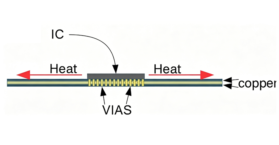
How Do Thermal Vias Improve PCB Heat Dissipation in Multi-layer Boards?
Thermal vias are critical for heat dissipation in PCB, especially multi-layer boards. They enable heat transfer between layers, preventing heat buildup in inner layers and hotspots on the top layermulti-layer boards often have limited surface area for heat dissipation, making thermal vias essential.
- Heat Transfer Between Layers: Thermal vias connect top-layer high-heat components to inner copper planes and the bottom layer, spreading heat across multiple layers to boost heat dissipation efficiency and reduce thermal buildup.
- Reduce Hotspot Formation: Thermal vias transfer heat from top-layer high-heat components to inner layers (with larger copper areas), evenly spreading heat and lowering hotspot temperatures, critical for preventing component damage.
- Enhance Thermal Conductivity: Solder or copper-filled thermal vias outperform empty vias by eliminating air gaps (thermal insulators), ensuring efficient heat transfer between layers and reducing thermal resistance.
- Optimal Placement: Install thermal vias directly under high-heat components (e.g., power chips, LEDs) to minimize heat travel. Use multiple small vias (instead of one large one) for even heat distribution and easier manufacturing.
- Design Considerations: Use 0.3–0.5 mm vias (optimal for performance/manufacturability), space them 1–2 mm apart under high-heat components, connect to large copper planes, and keep them away from signal traces to avoid interference.
What are the Top LED PCB Heat Dissipation Solutions?
LEDs generate significant heat relative to their size; poor heat dissipation in PCB reduces LED brightness, lifespan, and color consistency. LED PCB heat dissipation solutions focus on transferring heat from the LED chip to the environment, as LED chips are temperature-sensitive.
- Aluminum-Based MCPCBs: The most practical LED PCB solution, with aluminum core acting as an integrated heat sink to quickly transfer LED chip heat to the environment. Lightweight and cost-effective, suitable for most LED lighting scenarios (e.g., indoor lighting, small outdoor fixtures).
- Thermal Vias Under LEDs: Drill thermal vias directly under LED packages to transfer heat to inner/bottom copper layers, lowering chip temperature to extend lifespan and maintain brightness. For high-power LEDs, use multiple 0.3–0.5mm vias (spaced 1–2mm apart) for optimal heat transfer.
- Heat Sinks for High-Power LEDs: Attach finned heat sinks to LED PCBs for high-power arrays (street lights, industrial lighting). Apply thermal paste to ensure tight thermal contact, maximizing heat dissipation efficiency.
- PCB Layout Optimization: Space LEDs evenly (spacing ≥ 2x the LED size) to avoid hotspots, place them near PCB edges for better heat dissipation, and keep heat-generating components at a distance. Use wide copper traces (≥1mm per ampere for high-current paths) and connect them to large copper pours for effective heat spreading.
- Thermal Interface Materials (TIMs): Use thermal paste or pads between LED packages and PCBs/heat sinks to reduce thermal resistance. TIMs fill surface gaps, eliminating air pockets that trap heat and hinder heat transfer.
How to Reduce PCB Heat Dissipation Without Losing Performance?
Reducing heat dissipation in PCB does not require sacrificing performance. Optimizing component selection, design, and power management lowers heat generation while maintaining or improving system performance.
- Select Low-Power Components: Choose components with lower power consumption, such as low-power microcontrollers and efficient voltage regulators, to minimize heat generation. Prioritize components with higher efficiency ratings, as these devices convert more electrical energy into useful work rather than waste heat.
- Optimize Power Management: Utilize power management techniques to reduce power consumption during low-load periods. Common methods include voltage scaling, sleep modes, and pulse-width modulation (PWM). These strategies lower heat generation without compromising performance when full power is required.
- Improve PCB Trace Design: Use wider traces for high-current paths to reduce electrical resistance—lower resistance directly translates to less heat. Avoid long, narrow traces, as these increase resistance and create hotspots. Additionally, use copper pours for power and ground planes to spread heat evenly across the PCB.
- Use Thermal Management Features: Many electronic components come with built-in thermal management features, such as thermal shutdown and current limiting. These features automatically reduce heat generation when temperatures rise, helping prevent overheating without sacrificing system performance.
- Optimize Component Placement: Arrange PCB components to minimize heat overlap. Spread high-heat components apart and position them to leverage natural airflow. This layout strategy reduces heat buildup and allows components to operate at lower temperatures while maintaining full performance.
What Mistakes to Avoid in PCB Heat Dissipation Design?
Common mistakes in PCB heat dissipation design cause overheating, component failure, and costly redesigns. Avoiding these errors ensures heat dissipation in PCB is effective, reliable, and cost-efficient.
- Ignoring Thermal Requirements Early – Waiting until the final design stage to address heat dissipation leads to rushed, ineffective solutions. Incorporate thermal management into the initial design phase, considering component power consumption and layout.
- Overlooking Thermal Resistance – Failing to account for thermal resistance (e.g., between components and heat sinks, or PCB layers) leads to inaccurate temperature calculations. Always include thermal resistance values from component datasheets in your design.
- Using Inadequate Copper Area – Skimping on copper pour or using thin copper layers limits heat transfer. Use sufficient copper area on power and ground planes, and consider 2oz copper for high-heat areas.
- Poor Component Layout – Placing high-heat components too close together or in confined areas creates hotspots. Avoid placing heat-sensitive components near hotspots, and spread high-power components evenly across the PCB.
- Neglecting Airflow – Forgetting to design for airflow (natural or forced) traps heat in enclosed enclosures. Ensure the PCB and enclosure have adequate ventilation, and position components to not block airflow.
- Using Low-Quality Thermal Interface Materials – Cheap or low-performance TIMs fail to fill gaps effectively, increasing thermal resistance. Use high-quality TIMs (e.g., high-thermal-conductivity thermal paste) to ensure good thermal contact.
How to Test PCB Heat Dissipation Effectiveness?
Testing heat dissipation in PCB is critical to verify designs meet thermal requirements and prevent overheating. Effective testing identifies hotspots, measures temperature rises, and validates PCB heat dissipation techniques.
- Infrared (IR) Thermography – Use an IR camera to capture thermal images of the PCB during operation. This identifies hotspots, measures temperature distribution, and shows how heat spreads across the PCB. IR thermography is non-invasive and provides real-time thermal data.
- Thermocouple Measurements – Attach thermocouples to critical components (e.g., power chips, LEDs) and PCB surfaces for accurate temperature readings. Compare these readings to calculated values to validate design performance.
- Environmental Chamber Testing – Test the PCB in an environmental chamber to simulate real-world conditions (e.g., high ambient temperatures, humidity). This ensures heat dissipation in PCB is effective under extreme scenarios.
- Power Cycling Tests – Cycle the PCB between full power and low power to simulate real-world usage. Measure temperature changes during cycling to ensure heat dissipation handles varying power loads without overheating.
- Thermal Simulation Validation – Compare test results to thermal simulation data. Adjust the simulation model or PCB design if discrepancies exist, ensuring simulations accurately reflect real-world performance.
FAQs About Heat Dissipation in PCB
Q1: What is the maximum safe temperature for a PCB?
A1: The maximum safe temperature depends on components, but most PCBs operate safely between 0°C and 70°C. High-temperature PCBs (e.g., automotive, industrial) handle up to 125°C, but components like capacitors and resistors often have lower rated temperatures.
Q2: Can increasing copper thickness improve PCB heat dissipation?
A2: Yes, increasing copper thickness (e.g., 1oz to 2oz) improves thermal conductivity, allowing heat to spread more evenly. Thicker copper reduces resistance and boosts heat transfer, making it ideal for high-heat components.
Q3: Do thermal vias work in single-layer PCBs?
A3: Thermal vias work best in multi-layer PCBs but can transfer heat to a heat sink or PCB bottom surface in single-layer designs. In single-layer PCBs, they connect the top layer (components) to the bottom surface for environmental heat dissipation.
Q4: What is the best thermal interface material for PCB heat dissipation?
A4: The best TIM depends on the application, but thermal paste (1–5 W/m·K thermal conductivity) works for most PCB designs. Thermal pads suit uneven surfaces, while thermal adhesive is ideal for permanent heat sink attachment.
Q5: How does ambient temperature affect heat dissipation in PCB?
A5: Higher ambient temperatures reduce the temperature difference between the PCB and environment, slowing heat transfer. Additional techniques (e.g., fans, heat sinks) are needed in hot environments to prevent overheating.
Q6: Can component placement alone solve PCB overheating issues?
A6: Component placement is critical but often insufficient. High-power designs require additional techniques like heat sinks, thermal vias, or high-thermal substrates to ensure effective heat dissipation in PCB.
Q7: Is liquid cooling necessary for high-power PCBs?
A7: No, liquid cooling is not always needed. Most high-power PCBs work with heat sinks and forced air cooling. Liquid cooling is only required for extremely high-power designs (>100W) or enclosed systems with no airflow.
Q8: How often should PCB heat dissipation be tested?
A8: Test during the design phase, before production, and after any design changes. Field testing during operation is also recommended to ensure performance in real-world conditions.
You may also like


Tags: PCB Heat Dissipation, pcb heat dissipation calculation, PCB Heat Dissipation Techniques