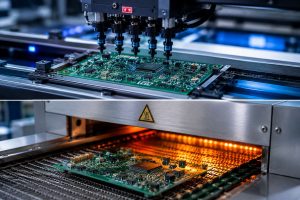
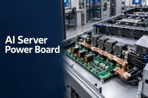
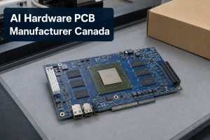
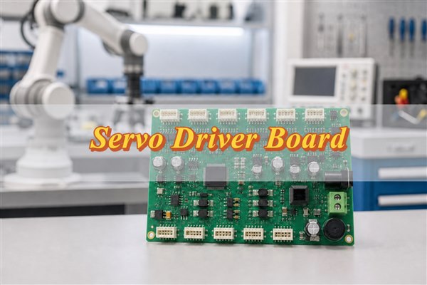
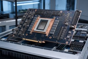
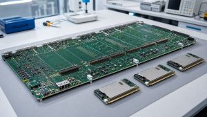
For teams searching AI hardware PCB manufacturer USA, the real challenge is not finding a company that can make a multilayer PCB. AI accelerators, edge-computing modules, machine-vision controllers, robotics platforms, and other high-performance hardware often combine fine-pitch BGAs, high-speed interfaces, controlled impedance, dense power delivery, and thermal constraints on the same board. The better supplier is the one that can support these requirements from prototype through repeat production.
EBest Circuit supports U.S. AI hardware projects through PCB fabrication, PCBA, component sourcing, testing, and box build from our manufacturing operations in China and Vietnam. If you already have a design, send your Gerber or ODB++, stack-up, BOM, assembly files, impedance requirements, quantity, and test requirements to sales@bestpcbs.com for an engineering review.
What Does an AI Hardware PCB Manufacturer Actually Need to Handle?
A manufacturer does not become an AI hardware PCB specialist simply by offering high-layer-count boards. The supplier needs to manage several constraints at the same time.
Typical AI hardware may include:
- GPU, FPGA, NPU, or SoC packages
- DDR memory
- PCIe, Ethernet, USB, MIPI, or SerDes interfaces
- Fine-pitch BGA escape routing
- Multiple power rails
- High-current processor supplies
- Controlled-impedance traces
- Dense passive components
- Thermal vias or copper reinforcement
- Tight SMT and inspection requirements
These requirements interact with one another.
Changing dielectric thickness can affect impedance. Increasing copper weight can alter the stack-up and etching process. A via change around a BGA may make routing easier but increase fabrication difficulty. A board can therefore be electrically correct and still be poorly suited to production.
Can the manufacturer evaluate fabrication, assembly, high-speed constraints, thermal structures, sourcing, and testability as one manufacturing problem?
That is a better indicator of whether the supplier is ready for a real AI hardware project.
What PCB Technologies Are Commonly Required for AI Hardware?
Not every AI board needs HDI, Rogers material, or heavy copper. PCB technology should follow the actual electrical, thermal, routing, and mechanical requirements.
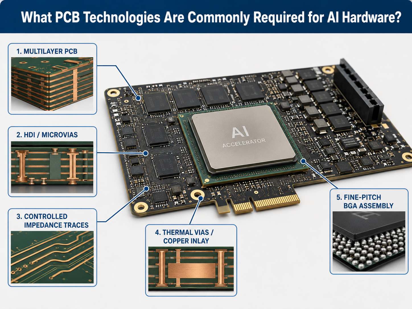
| AI Hardware Need | Common PCB Solution |
|---|---|
| GPU / FPGA / NPU | Multilayer PCB |
| PCIe / SerDes / Ethernet | Controlled impedance |
| Fine-pitch BGA | HDI / microvias |
| High current | Thicker copper / power planes |
| High heat density | Thermal vias / copper inlay |
| Compact edge AI | HDI + fine-pitch SMT |
| RF or very high-speed section | Low-loss laminate |
| High I/O count | More routing layers |
Over-specification can raise cost without improving the finished product.
If a design works reliably on a well-engineered high-Tg FR-4 stack-up, moving the entire PCB to a premium low-loss laminate may not be necessary. The same applies to HDI. It should be used where package pitch, routing density, or board size requires it.
A capable manufacturer should be able to explain where an advanced process is necessary and where the PCB can remain simpler.
What Should USA Companies Look for in an AI Hardware PCB Manufacturer?
Start with the actual board rather than a generic factory capability list.
For an AI hardware project, check four things:
- PCB fit: layer count, HDI structure, via-in-pad, impedance, material, copper weight, and thickness.
- Assembly fit: fine-pitch BGA, QFN/LGA, double-sided SMT, and high thermal-mass boards.
- Inspection and test: SPI, AOI, X-ray, electrical test, ICT, programming, and functional test where required.
- Scale-up support: BOM sourcing, revision control, traceability, test fixtures, repeat orders, and volume ramp-up.
Before placing an order, ask the supplier to confirm the critical requirements against your released Gerber, stack-up, BOM, and assembly data.
The best supplier is not the one with the longest capability list, but the one whose process window matches your board.
Top 15 AI Hardware PCB Manufacturers in the USA
The U.S. has several PCB and electronics manufacturers capable of supporting complex computing, high-speed digital, HDI, advanced assembly, and high-reliability hardware.
The list below is intended as a practical supplier-comparison starting point rather than a strict ranking. Some companies focus more heavily on bare PCB fabrication, while others provide broader PCBA or EMS services.
| Manufacturer | Key Strength | Good Fit For |
|---|---|---|
| TTM Technologies | Advanced multilayer, HDI | Servers, accelerators |
| Sanmina | Complex high-layer PCB | High-end computing |
| Summit Interconnect | HDI, RF, rigid-flex | Advanced NPI |
| AdvancedPCB | HDI, impedance, quick-turn | Prototype to production |
| Sierra Circuits | UHDI, prototype engineering | Dense AI boards |
| Calumet Electronics | Advanced domestic PCB | High-reliability projects |
| American Standard Circuits | UHDI, RF, thermal PCB | Mixed high-speed designs |
| Bay Area Circuits | Quick-turn high-speed PCB | Engineering prototypes |
| RUSH PCB | HDI and turnkey PCBA | Fast prototype builds |
| Epec | Broad PCB technologies | Industrial electronics |
| MacroFab | Digital PCBA manufacturing | Startup scaling |
| Green Circuits | Complex SMT and testing | Edge AI / robotics |
| SVTronics | PCB + PCBA + integration | Complete hardware builds |
| Creation Technologies | Large-scale EMS | Production programs |
| Sierra Assembly Technology | Quick-turn assembly | Low-volume complex PCBA |
The next step is not simply choosing the largest company in the table. Narrow the list according to the actual PCB and production model.
If the project requires U.S.-only manufacturing because of contractual, security, ITAR, or supply-chain requirements, domestic production may be mandatory.
If it does not, compare suppliers on:
- Technical fit
- Engineering support
- Lead time
- Scalability
- Component sourcing
- Production cost
The practical sourcing question is:
Which supplier can build this board correctly now and continue supporting it when volume increases?
High-Speed PCB Manufacturing for AI Accelerators and Computing Hardware
High-speed interfaces are one of the main reasons AI hardware becomes difficult to manufacture.
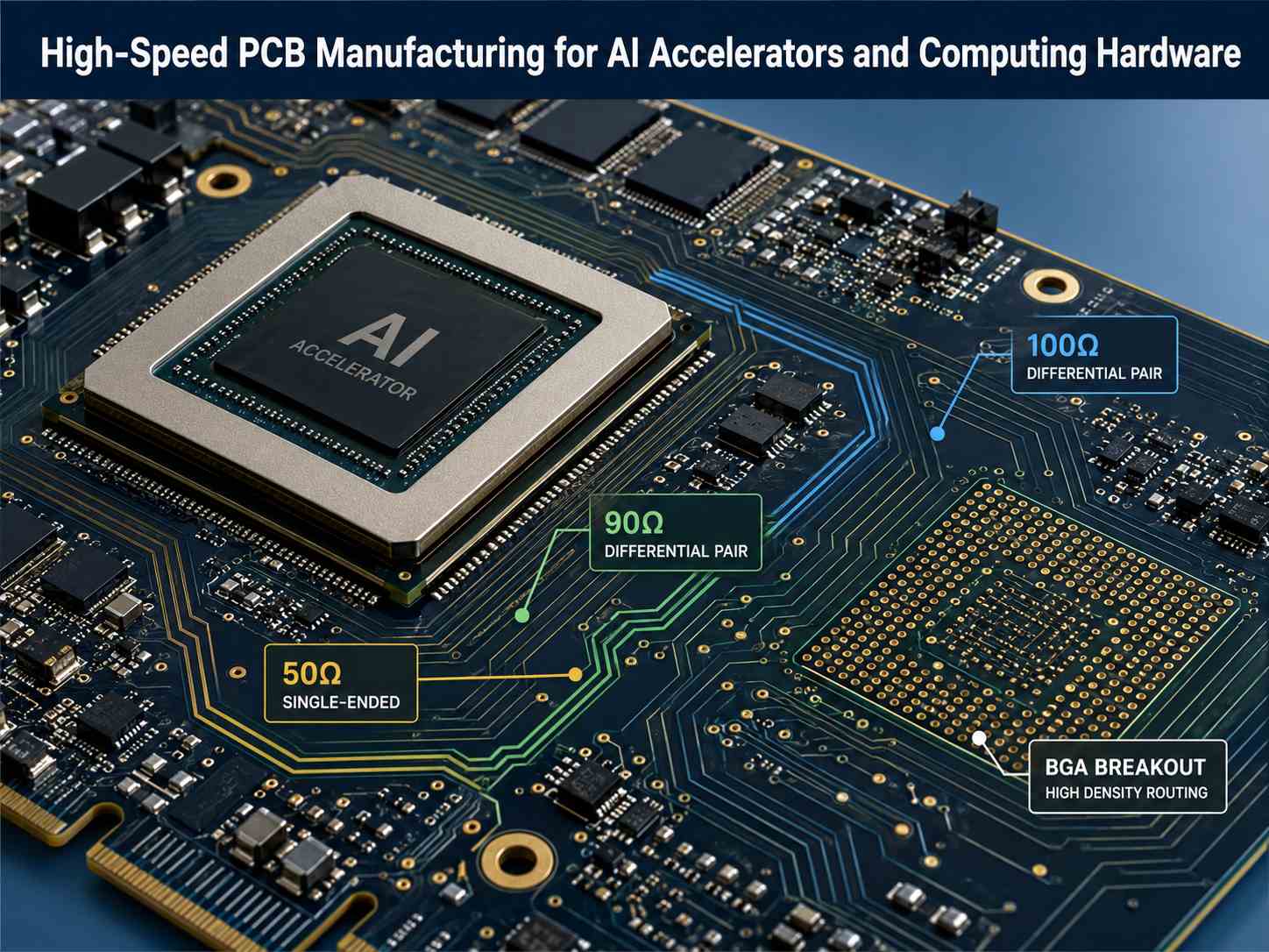
Typical interfaces include:
- PCIe
- DDR
- Ethernet
- SerDes
- USB
- MIPI
- High-speed clock networks
Common impedance targets include 50 Ω single-ended and 90 Ω or 100 Ω differential, although the customer’s released design requirement should always determine the final specification.
For a controlled-impedance RFQ, useful manufacturing data includes:
- Target impedance
- Signal layer
- Reference plane
- Trace width and spacing
- Copper thickness
- Dielectric thickness
- Material grade
Material selection also matters. High-Tg FR-4 is suitable for many AI boards, while lower-loss laminates become more useful when channel-loss requirements are tighter.
At EBest Circuit, we normally ask for more than Gerber files when reviewing a high-speed board. Providing the stack-up, material grade, dielectric thickness, copper weight, and target impedance allows our engineering team to review the structure before fabrication.
How Should Power and Thermal Management Be Built into an AI PCB?
A high-performance processor can create significant electrical and thermal load in a relatively small PCB area.
The board may therefore need to support both current delivery and heat spreading.
Common options include:
- Wide copper areas
- Solid power and ground planes
- Higher copper weight
- Thermal-via arrays
- Local copper spreading
- Copper coin or copper inlay
The correct solution depends on the heat path.
Thermal vias are useful when heat needs to move vertically through the PCB. Copper inlay becomes more attractive when a component requires a stronger direct thermal path.
Heavy copper can also support high-current sections, but increasing copper thickness affects etching, lamination, resin fill, and line-width control. It should therefore be considered during stack-up development rather than added late in the purchasing process.
For a useful thermal review, provide the manufacturer with:
- Copper weight
- High-current net information
- Major heat sources
- Thermal-via requirements
- Maximum board thickness
- Heat-sink or enclosure constraints
This gives the factory enough information to identify manufacturing conflicts before production.
Why HDI and Fine-Pitch Assembly Matter in Compact AI Hardware
Edge AI devices, robotics controllers, embedded vision systems, and smart cameras often need a large amount of processing capability in a small enclosure.
That creates dense routing around BGA devices.
HDI can provide more routing freedom through:
- Laser microvias
- Blind and buried vias
- Via-in-pad
- Sequential lamination
- Smaller capture pads
Microvias around 150 μm or below are commonly used in HDI construction, although the correct size depends on dielectric thickness, pad geometry, aspect ratio, and reliability requirements.
PCB fabrication is only one part of the problem. The assembly process must also control:
- Solder paste
- Placement accuracy
- Reflow profile
- BGA warpage
- Moisture-sensitive devices
- Hidden solder joints
SPI is useful before placement. AOI checks visible assembly defects, while X-ray is more useful for BGA, QFN, and other bottom-terminated packages.
For dense AI hardware, having PCB fabrication and PCBA managed by the same manufacturing partner can also reduce handoff risk when a yield issue appears.
PCB Assembly and Component Sourcing for AI Hardware Projects
A complex BOM can delay an AI hardware project even when the PCB itself is ready.
Common devices include:
- FPGA, NPU, MCU, or SoC
- DDR and Flash memory
- PMIC
- Ethernet PHY
- MOSFETs
- Clock ICs
- Sensors
- High-speed connectors
Before production, the BOM should be checked for:
- Manufacturer part number
- Lifecycle status
- Stock availability
- MOQ
- Approved alternatives
- MSL level
- Programming requirements
Traceability is also important for expensive processors, memory devices, and programmable components.
One practical model for early production is PCB kitting with mixed sourcing. A customer may consign the key FPGA, processor, or memory devices while allowing the PCBA supplier to source standard resistors, capacitors, power components, and connectors.
EBest Circuit supports turnkey, partial-turnkey, and customer-consigned assembly, so the sourcing model can change as the project moves from prototype into production.
How Can DFM Reduce AI Hardware Prototype Risk?
DFM should reduce the chance of discovering expensive manufacturing issues after the boards are already built.
For an AI hardware PCB, useful DFM checks include:
- Trace and spacing
- Annular ring
- Hole-to-copper clearance
- BGA breakout
- Microvia structure
- Via-in-pad
- Copper balance
- Stack-up
- Controlled impedance
- Solder-mask openings
- Component clearance
- Panelization
The important distinction is that manufacturable does not always mean production-ready.
A BGA breakout may technically be buildable but unnecessarily expensive. A stack-up may work for a prototype while leaving very little process margin for repeat production. A component placement may look acceptable in CAD but create inspection or rework problems after assembly.
At EBest Circuit, our DFM review looks at the PCB and PCBA together rather than treating fabrication as a separate step. For AI hardware projects, we review the stack-up, via structure, BGA escape routing, impedance requirements, copper distribution, solder-mask design, assembly clearance, and panelization before production. When HDI, fine-pitch BGA, heavy copper, or low-loss materials are involved, we also check whether the selected process is practical for both prototype and later production.
The better target is a PCB that can be fabricated, assembled, inspected, tested, and repeated consistently as volume increases.
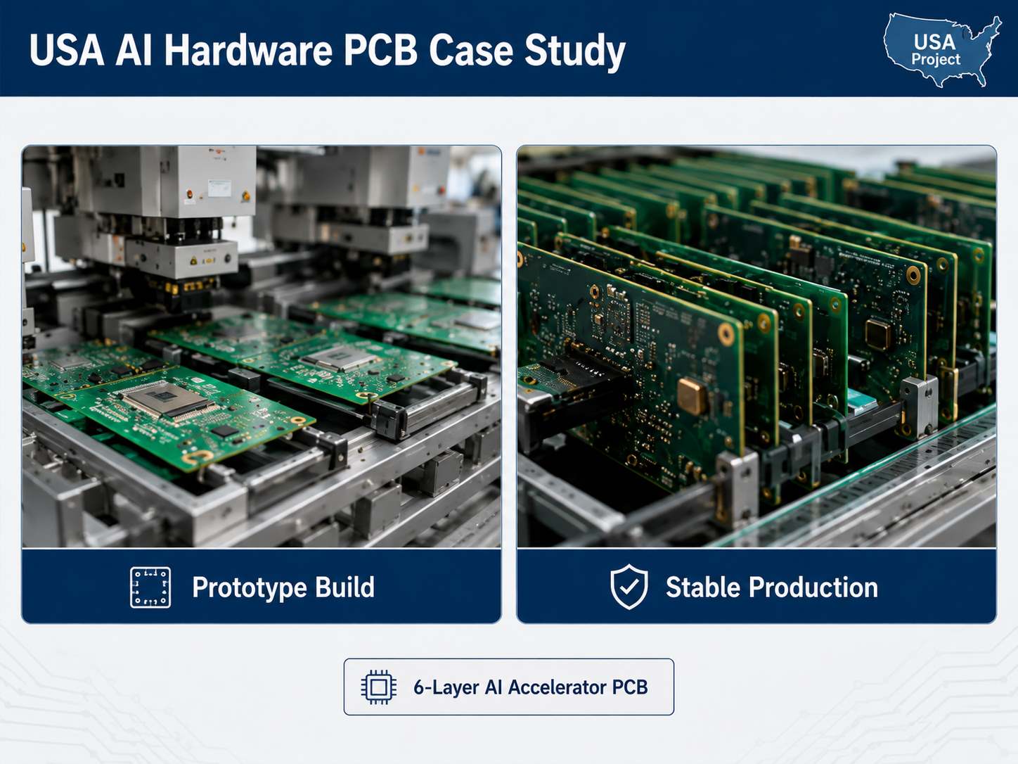
USA AI Hardware PCB Case Study: From Prototype DFM to Stable Production
A U.S. customer required a 6-layer PCB for an AI accelerator. The board used FR-4 Tg 180°C with a finished thickness of 1.0 ± 0.1 mm, while the manufacturing requirements included 50 Ω impedance, resin-filled vias, Class 3 hole copper, serialization, and board-warpage control.
Project Specifications
| Item | Requirement |
|---|---|
| Layer count | 6 layers |
| Material | FR-4, Tg 180°C |
| Thickness | 1.0 ± 0.1 mm |
| Copper | 1 oz each layer |
| Impedance | 50 Ω |
| Via treatment | Resin-filled and plated flat |
| Hole copper | ≥20 μm |
| Surface finish | ENIG, 5 μin Au |
| Serialization | LP-01# to LP-20# |
Challenge
The thin 6-layer construction required careful stack-up, copper balance, and panel control to reduce bow and twist while maintaining 50 Ω impedance. All vias also required resin filling and plating, and only the individual serial numbers could remain on the silkscreen.
EBest Circuit Solution
Before production, we reviewed the stack-up, impedance structure, via process, panelization, and marking requirements together. Production data was then sent to the customer for approval before fabrication.
Result
The project established a controlled manufacturing setup for repeat builds, with the key impedance, via, hole-copper, serialization, and flatness requirements defined before production release.
For AI hardware PCB prototypes, stable production starts with controlling the manufacturing details before the first build.
What Testing Should Be Used for AI Hardware PCB and PCBA?
Testing should follow the manufacturing stage and the actual failure risk.
| Stage | Typical Check |
|---|---|
| Bare PCB | Electrical test |
| Impedance PCB | Impedance test |
| Paste printing | SPI |
| SMT | AOI |
| BGA / QFN | X-ray |
| Finished PCBA | ICT / functional test |
Functional testing should be tied to the product rather than reduced to a simple power-on check.
Depending on the hardware, a test procedure may verify:
- Power rails
- Current consumption
- Boot status
- Firmware programming
- Ethernet
- USB
- Sensors
- Display output
- Fan control
If the customer already has a fixture or test procedure, it should be included in the RFQ package. If not, the test method should be discussed before volume production begins.
Prototype or Mass Production: Which Manufacturing Model Fits Your AI Hardware Project?
AI hardware manufacturing changes as the product moves through development.
Prototype
The priorities are speed, engineering feedback, and design learning.
At this stage:
- Quantities are small
- Revisions are frequent
- The BOM may still change
- DFM feedback often matters more than final unit cost
EVT / DVT / PVT
The manufacturing process should begin to stabilize:
- Stack-up
- Material
- BOM
- Assembly process
- Test fixture
- Programming
- Work instructions
This is where many issues that were acceptable on five boards become expensive.
Volume production
The focus shifts toward:
- Yield
- Repeatability
- Traceability
- Component continuity
- Test coverage
- Cost
- Capacity
If the product is expected to scale, supplier selection should consider the next manufacturing stage as well as the current one.
Changing PCB or PCBA suppliers immediately after prototype validation can add another engineering qualification cycle and slow production ramp-up.
Why USA AI Hardware Companies Work With EBest Circuit
If your project requires U.S.-only manufacturing, EBest Circuit may not be the right fit because our manufacturing operations are based in China and Vietnam.
For U.S. companies open to global manufacturing, we offer one manufacturing partner for complex PCB fabrication, component sourcing, assembly, testing, and production scaling.
Our capabilities relevant to AI hardware include:
- High-layer-count and HDI PCB
- Controlled-impedance and high-speed PCB
- Rogers and hybrid constructions
- Heavy copper and copper inlay
- Fine-pitch BGA assembly
- SPI, AOI, X-ray, ICT, and functional testing
- Turnkey component sourcing and programming
- Prototype through volume production
For an AI accelerator, edge AI device, machine-vision controller, or other high-density computing board, we prefer to review the actual design rather than qualify the project from a generic capability list.
Send us the Gerber or ODB++, stack-up, BOM, impedance requirements, assembly files, and test requirements. Our engineering team can check whether the PCB construction, BGA routing approach, materials, copper requirements, assembly process, and test plan fit the intended manufacturing process before production.
Our quality systems cover ISO 9001, ISO 13485, IATF 16949, and AS9100D requirements, supporting projects that require controlled and traceable manufacturing processes.
What Should You Send for an AI Hardware PCB Quote?
A complete RFQ makes the engineering review faster and reduces assumptions in the quotation.
For PCB fabrication, send:
- Gerber or ODB++
- Fabrication drawing
- Stack-up
- Material requirement
- Copper weight
- Surface finish
- Via specification
- Impedance requirements
- Quantity
For PCBA, add:
- BOM
- Pick-and-place file
- Assembly drawing
- Programming files
- Test requirements
For high-speed boards, also include the target impedance, material grade, dielectric thickness, copper weight, and relevant interface information.
If the design is still in development, you do not need to wait until every production document is complete. The latest Gerber, BOM, stack-up, quantity, and key requirements are usually enough for an initial manufacturing review.
FAQs About AI Hardware PCB Manufacturing
1. What type of PCB is used in AI hardware?
AI hardware commonly uses multilayer rigid PCB, HDI PCB, rigid-flex PCB, or a combination of high-speed and high-current PCB technologies. The correct construction depends on processor package, routing density, interface speed, current, and thermal requirements.
2. Can AI hardware PCBs use standard FR-4?
Yes. Many AI boards can use high-Tg FR-4. A low-loss laminate is normally justified when high-speed channel loss, impedance stability, or frequency requirements exceed what the selected FR-4 system can comfortably support.
3. Do AI accelerator boards require HDI?
Not always. HDI is most useful when fine-pitch BGAs, high I/O density, limited board area, or difficult escape routing make conventional through-via construction inefficient.
4. What materials are suitable for high-speed AI PCBs?
High-Tg FR-4 works for many applications. Low-loss laminates, Rogers materials, or hybrid stack-ups can be considered when signal-loss requirements are more demanding.
5. Can EBest Circuit manufacture AI hardware PCBs for USA customers?
Yes. We support U.S. customers through our China and Vietnam manufacturing operations, covering PCB fabrication, component sourcing, PCBA, inspection, testing, programming, and box build.
6. What files are required for an AI hardware PCB quotation?
For PCB fabrication, send Gerber or ODB++, stack-up, specifications, material, copper weight, impedance targets, quantity, and finish requirements. For PCBA, also provide the BOM, pick-and-place file, assembly drawing, programming files, and test requirements.
Ready to Discuss Your AI Hardware PCB Project?
If you are developing an AI accelerator, edge AI device, machine-vision system, robotics controller, AI computing module, or other high-performance hardware, send your Gerber or ODB++, stack-up, BOM, assembly files, impedance requirements, quantity, and test requirements to sales@bestpcbs.com. Our engineering team can review the project before quotation and help identify PCB fabrication, assembly, sourcing, or testing issues that may affect prototype or volume production.
If you would like to evaluate our manufacturing capabilities in person, you are welcome to visit our factory. We can arrange a factory tour for your engineering or sourcing team to review our PCB fabrication, SMT assembly, inspection, testing, and quality-control processes. To evaluate EBest Circuit for your AI hardware PCB manufacturer USA project, send project files or arrange a factory visit through sales@bestpcbs.com.