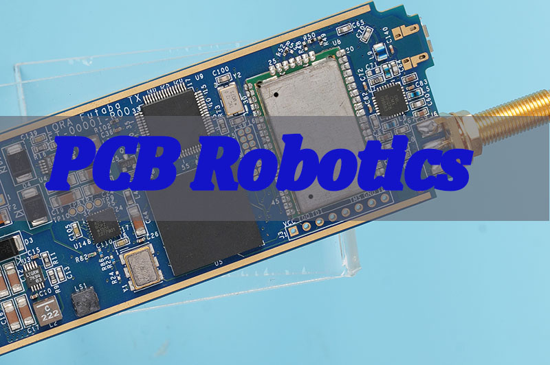
AI robotics PCB manufacturing brings computing, vision, sensing, motion control, communications, and power electronics into one hardware program. A computing board may require dense BGA breakout and controlled impedance, while motor-control and power-distribution boards must carry pulsed current without disturbing sensors or data links.
Prototype success does not guarantee repeat production. Mixed file revisions, unavailable processors, fine-pitch solder defects, motor-related power noise, concentrated heat, and incomplete test limits can cause rework, inconsistent builds, or delayed product validation.
EBest Circuit reviews the complete manufacturing package. We align PCB data, BOM, placement, assembly, programming, inspection, and customer-defined test requirements before production, then support fabrication and assembly from prototype through volume builds. Send your Gerber/ODB++, BOM, quantity, assembly files, and test scope to sales@bestpcbs.com for a free DFM review and quotation.
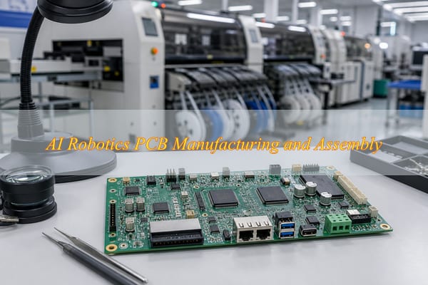
What Types of PCBs Are Used in AI Robotics Systems?
Board partitioning should follow system function. An AI robotics system may distribute computing, sensing, motion, power, and communication across several PCBs or combine selected functions on one board. Common PCB categories include:
| PCB Type | Main Function | Typical Requirements |
| AI computing PCB | Runs AI inference, control algorithms, and data processing | Dense BGA routing, high-speed interfaces, controlled impedance, thermal management |
| Vision PCB | Connects cameras and image sensors | High-speed interfaces, low-noise power, compact layout |
| Sensor PCB | Collects encoder, IMU, force, distance, or environmental data | Low-noise analog circuits, stable references, reliable sensor interfaces |
| Robot control PCB | Coordinates motion, I/O, and communications | MCU/FPGA integration, CAN/Ethernet interfaces, mixed-signal layout |
| Motor control PCB | Drives BLDC motors, servos, and other actuators | Higher current, MOSFET thermal paths, reinforced power connections |
| Power distribution PCB | Converts and distributes battery or DC input power | Current-carrying capacity, power connectors, protection devices, thermal control |
| Communication PCB | Handles wired or wireless links | Controlled impedance, RF requirements, connector and antenna constraints |
A humanoid robot may place motor-control boards close to individual joints while keeping AI computing and vision processing in the head or torso. An autonomous mobile robot may use a central computing board connected to separate motor, navigation, power, and communication boards.
The exact architecture depends on processing load, mechanical space, cable length, current distribution, and serviceability. Before releasing each board, verify its power budget, interface ownership, connector path, mounting envelope, and replacement boundary; an unclear split can create overloaded connectors, duplicated power conversion, or interfaces that cannot be tested independently.
Which Components and Interfaces Are Commonly Used on AI Robot PCBs?
Package mix and interface speed drive PCB complexity. AI robot PCBs may combine processors, memory, sensors, power devices, and communication circuits whose electrical, assembly, and test-access requirements must be reviewed together.
Common components include:
- AI processors and SoCs: Run computer vision, neural-network inference, navigation, and higher-level decision functions.
- MCUs and FPGAs: Handle real-time I/O, timing-sensitive control, motion functions, and interface management.
- DDR memory and flash storage: Support high-bandwidth processing and local data storage.
- Image sensors and camera-related ICs: Support RGB, depth, stereo, and machine-vision systems.
- IMUs and motion sensors: Measure acceleration, angular rate, orientation, or movement.
- Motor drivers and MOSFETs: Switch current for BLDC motors, servos, pumps, and actuators.
- Encoders and feedback devices: Provide position, speed, and motion feedback.
- DC-DC converters and regulators: Generate stable power rails for processors, sensors, and communication circuits.
Common interfaces include:
- CAN and CAN-FD: Connect distributed motor and control nodes.
- Ethernet: Carries higher-bandwidth data between computing and control modules.
- USB: Supports peripherals, cameras, configuration, and data transfer.
- PCIe: Supports high-bandwidth expansion or computing modules where the architecture requires it.
- High-speed camera interfaces: Carry image and vision data between sensors and processors.
- Wi-Fi and Bluetooth: Support wireless communication, configuration, and telemetry.
For engineering and sourcing teams, the important cost and schedule drivers are package pitch, routing density, current, and interface speed rather than the total component count. Include these constraints in the RFQ so suppliers quote the required stackup, inspection, and assembly route instead of pricing from board dimensions alone.
Which PCB Technologies Are Needed for AI Processors, Vision Sensors, and Motion Control?
Each robot function owns different PCB requirements. AI processing is dominated by BGA breakout, memory routing, power integrity, and heat; machine vision by low-noise power and camera-link continuity; and motion control by pulsed current, switching loops, protection, and thermal paths.
- AI processor and memory routing: Start from the released processor escape pattern, DDR topology, interface constraints, and stackup. Use HDI, laser microvias, or filled via-in-pad only when the BGA pitch and routing channels cannot be completed with a simpler through-via structure. Verify impedance coupons where specified and review the routed design for reference-plane continuity and excessive via transitions before fabrication.
- Processor power integrity: Separate core, memory, I/O, and auxiliary rails according to the processor power tree. Place the required decoupling close to the relevant power balls, provide low-impedance return paths, and size regulator and copper paths for startup and workload transients. Validate rail sequencing, ripple, droop, and current at defined operating states rather than checking only idle voltage.
- Processor thermal path: Move package heat into the PCB copper, thermal vias, heat spreader, or chassis interface defined by the mechanical design. Confirm thermal-pad solder coverage and interface contact during assembly, then measure component temperature under sustained inference and communication loads to check throttling margin.
- Vision sensor signal path: Route MIPI, LVDS, USB, Ethernet, or other camera links to their specified impedance, skew, and reference requirements. Maintain a continuous return structure across connectors and layer transitions, and keep camera clocks and data pairs away from motor-switching nodes. Verify the interface with captured images and error monitoring under representative cable length and frame rate.
- Vision sensor power and grounding: Supply image sensors, clocks, and analog references from low-noise rails with local filtering and decoupling placed at the receiving devices. Keep shared impedance with motor and power-conversion returns out of the sensor reference path. Compare image noise, dropped frames, and sensor data with motors disabled and operating to identify coupling.
- Motion-control power stage: Size MOSFET, driver, shunt, connector, copper, and plated transitions from continuous current, peak current, duty cycle, and fault-clearing requirements. Keep the switching and gate-drive loops compact, separate sensitive encoder and communication routes, and provide a defined heat path from the power devices. Validate current waveform, rail disturbance, device temperature, and protection response at startup, reversal, braking, stall, and commanded load changes.
Assign each requirement to one board function and one verification method so computing, vision, and motion-control rules are not copied across unrelated boards.
How Should Robot Control PCBs Handle Motor Current, Power Noise, and Signal Integrity?
A robot control PCB must prevent motor and actuator loads from disturbing processors, sensors, and communication circuits. Current changes during motor startup, braking, reversal, and torque changes can create voltage drop, switching noise, and ground disturbance.
- Current-path sizing: Size power traces and copper areas from both continuous and peak current so the conductors match the actual load.
- Layer-change capacity: Use sufficient copper and plated connections where current changes layers to avoid narrow current bottlenecks.
- Switching-loop control: Keep high-current switching loops compact around MOSFETs, motor drivers, and local decoupling to reduce conducted and radiated noise.
- Power and signal separation: Route motor-current paths away from low-level analog and sensor circuits to reduce measurement disturbance.
- Return-path continuity: Maintain continuous return paths under high-speed signals so return current does not detour around plane gaps.
- Bulk energy storage: Place bulk capacitance close to high-current loads to limit supply collapse during rapid load changes.
- Local high-frequency decoupling: Place local decoupling close to processors, drivers, and interface ICs to reduce high-frequency supply noise.
- Connector current limit: Check connector current rating together with PCB copper capacity because an undersized connector can become the limiting point.
- Sensitive-node clearance: Keep switching nodes away from encoder inputs, analog sensors, clocks, and sensitive communication lines.
A controller that operates normally on a bench may reset when several motors accelerate together. Power-rail drop, connector resistance, inadequate bulk capacitance, or poor current return paths should be checked before treating the problem as a processor or firmware failure.
How Are HDI PCBs for AI Robotics Manufactured?
Specify HDI only when the routed design needs it. Engineers should confirm that through vias cannot complete the BGA breakout or high-speed routing. Procurement should compare the proposed microvia structure, lamination count, via fill, registration plan, test evidence, and repeat-production controls.
The released stackup should identify core and prepreg construction, finished copper, dielectric spacing, impedance requirements, microvia layers, and permitted via structures. These inputs let the supplier confirm manufacturability and allow the buyer to see which fabrication steps and inspections are included in the quotation.
- Microvia structure: State the start and stop layers, finished diameter, pad size, and whether the vias are staggered, stacked, filled, or capped. This prevents different suppliers from quoting different constructions under the same HDI label.
- Via-in-pad requirement: Identify the BGA, LGA, or thermal-pad locations that require filling and planarization. Ask the supplier to confirm the fill and surface preparation included in the build.
- Lamination count: Request the proposed build sequence when several drilling and lamination cycles are required. Additional cycles affect cost, lead time, registration risk, and the ease of repeating the design.
- Fine-line capability: Compare the released trace, space, annular-ring, and registration requirements with the supplier’s reviewed manufacturing limits for this stackup rather than relying on a general capability table.
- Plating evidence: Define the required finished copper and hole requirements and agree on the coupon, microsection, or inspection evidence needed for lot acceptance.
- Impedance verification: Provide target values, tolerances, reference layers, and coupon requirements. Request the measured coupon result when controlled impedance is part of the order.
- Registration review: Ask for a DFM response covering microvia-to-pad alignment and layer-to-layer registration where the design uses tight capture pads or stacked structures.
- Bare-board release: Include electrical testing for opens and shorts and define any additional dimensional, impedance, or microsection records required before assembly.
Request a reviewed stackup before tooling. If a simpler via structure completes the routing, remove unnecessary lamination cycles, cost, and supply risk.
What Assembly Controls Are Required for AI Processors, BGAs, Memory, and Fine-Pitch Components?
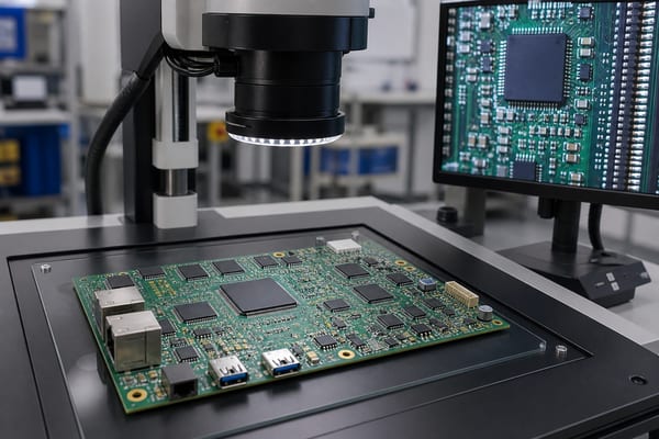
Fine-pitch packages need an agreed assembly and inspection plan. Engineers should identify package-specific risks, while procurement should confirm which controls and records are included in the quotation for processors, DDR devices, QFNs, LGAs, BGAs, and small passive components.
- Package-data confirmation: Supply manufacturer part numbers, approved footprints, polarity, and package drawings. Require discrepancies to be raised before stencil or placement-program release.
- Moisture-sensitive handling: Identify moisture-sensitive devices and request handling records when storage exposure or baking can affect package integrity and solderability.
- Stencil review: Ask the assembler to review stencil thickness and critical apertures against the complete package mix, especially when a large thermal pad sits beside fine-pitch passives.
- Paste inspection scope: Define whether SPI is required for the pilot and production lots and which paste defects or trends must stop the build before placement.
- First-article evidence: Agree on the component identity, polarity, placement, and workmanship checks that must be completed before the balance of the lot proceeds.
- Reflow confirmation: Request confirmation that the profile is developed around board thermal mass, solder-paste requirements, and component temperature limits.
- Hidden-joint inspection: Specify X-ray coverage and acceptance criteria for BGA, LGA, QFN, and other bottom-terminated packages that AOI cannot assess.
- Thermal-pad acceptance: Define how solder coverage or voiding beneath exposed pads will be evaluated when it affects heat transfer or electrical grounding.
- Mixed-technology assembly: Identify press-fit, selective-soldered, or manually installed power connectors so their tooling, sequence, and inspection are included in the quote.
For a valid price comparison, require each supplier to state the SPI, AOI, X-ray, first-article, programming, and test scope. Before release, confirm that the PCB data, BOM, CPL, assembly drawing, approved alternatives, and firmware identify the same revision.
How Should Thermal Performance Be Managed in AI Robotics PCB Assemblies?
Concentrated heat needs a continuous thermal path. Heat from AI processors, regulators, motor drivers, MOSFETs, and other power devices must move through the package connection, PCB copper and vias, and any heat spreader or enclosure interface defined by the mechanical design.
- Copper heat spreading: Use larger copper areas around power devices to spread heat beyond the package footprint.
- Thermal-via path: Add thermal vias beneath exposed thermal pads when heat needs to move into internal or opposite-side copper.
- Copper selection: Select copper thickness according to actual current and thermal requirements instead of increasing copper across the entire board.
- Thermal-pad paste control: Control solder paste beneath large thermal pads so excessive voiding does not interrupt the intended heat path.
- Mechanical heat transfer: Provide heat-sink or chassis contact when the mechanical design uses conductive cooling.
- Sensor placement: Keep temperature-sensitive sensors away from concentrated heat sources where possible.
- Thermal interface definition: Define thermal interface material thickness and contact area when the PCB transfers heat to a metal enclosure or heat spreader.
- Loaded temperature validation: Verify temperature under representative processor and motor loads rather than relying only on idle measurements.
A processor can remain stable during short functional testing and still throttle or fail during sustained inference workloads. Thermal validation therefore needs to reflect the real operating duty cycle.
How Should Vibration and Mechanical Stress Be Controlled in Robotics PCB Assemblies?
Control mechanical loads at their entry and stress points. Vibration, shock, cable movement, connector loading, and repeated motion should be addressed at mounting points, heavy components, connectors, board edges, and flexible interconnects.
- Mounting-hole placement: Position mounting holes so mechanical loads do not produce excessive board flex around BGAs or other large packages.
- Heavy-component support: Avoid leaving heavy inductors, transformers, capacitors, or connectors unsupported in high-vibration areas.
- Connector retention: Use connectors with suitable retention when repeated motion could loosen a friction-fit connection.
- Cable strain relief: Provide cable strain relief so cable movement is not transferred directly into solder joints.
- Loaded-connector reinforcement: Reinforce through-hole or mechanically loaded connectors when insertion or cable force justifies it.
- Stress-zone clearance: Keep mechanically sensitive components away from board edges, mounting stress areas, and enclosure interference zones.
- Staking or underfill decision: Use staking or underfill only where component mass, vibration, or qualification requirements justify the added process.
- Coating keep-outs: Define coating keep-out areas before conformal coating when connectors, test points, or thermal contact surfaces must remain exposed.
- Rigid-flex bend control: When rigid-flex is used, match bend radius, flex length, copper construction, and bend location to the real mechanical movement.
Rigid-flex is a special interconnect option for suitable mechanical structures. It should not be treated as a standard PCB type required by all AI robotics products.
How Are AI Robotics PCB Assemblies Inspected, Programmed, and Functionally Tested?
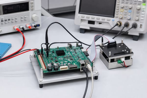
Buyers need a test plan that connects each risk to evidence. Before ordering, engineering should define the functions and limits that matter, procurement should confirm what the supplier includes, and both teams should agree on the records delivered with the lot. “AOI and functional test included” is not enough unless the coverage and acceptance criteria are stated.
- Define bare-board evidence: Require electrical testing for opens and shorts and identify any stackup, dimensional, finish, impedance-coupon, or microsection records needed for acceptance. Procurement can then confirm whether those records are included in the PCB price.
- Set paste-control expectations: Identify packages or thermal pads that justify SPI and agree on the defects or trends that stop the line. The supplier should explain how paste results are tied to the released stencil and board revision.
- Approve first-article coverage: Specify the identity, polarity, orientation, placement, and visible-joint checks required before the remaining quantity is assembled. Ask for a recorded approval rather than relying on an undocumented operator check.
- Request hidden-joint evidence: Map BGA, LGA, QFN, and bottom-terminated pads to X-ray coverage and project acceptance criteria. A representative image is useful only when it identifies the board, package, lot, and decision basis.
- Choose unpowered checks: Use ICT, flying probe, or a dedicated fixture only where test access and circuit behavior support useful limits. Engineering should define which nets, values, or rail resistances can distinguish an assembly fault from normal component tolerance.
- Control firmware identity: Provide the approved bootloader, MCU, FPGA, or configuration package with tool settings and a version or checksum. Require the programming result to be linked to the lot or serial number when traceability matters.
- Define functional acceptance: State input voltage, power sequence, interfaces, loads or simulators, expected responses, and pass/fail limits. Request measured values for critical functions instead of accepting a record that only says “powered on.”
- Agree on failure handling: Define which test records accompany the lot and how failures, rework, and retest are logged. This prevents repeated testing from hiding intermittent faults and gives engineering data for corrective action.
Engineering can build the functional-test scope from the board’s released interfaces and system risks:
- Power acceptance: State startup sequence, rail limits, expected current, reset behavior, and abnormal-current response at defined input conditions.
- Communication acceptance: Name each CAN, CAN-FD, Ethernet, USB, or other interface, together with the messages, speed, termination, and error criteria to be exercised.
- Sensor and encoder acceptance: Provide known input states or simulator signals, expected readings, range limits, and fault responses.
- Motor-output acceptance: Define enable, direction, PWM or command response, feedback, protection behavior, and the safe load or simulator used at PCBA level.
- Vision-interface acceptance: Define camera detection, link mode, frame transfer, and error reporting; reserve optical alignment and final image-quality acceptance for the assembled robot where appropriate.
- Service-function acceptance: Identify programming ports, storage, GPIO, indicators, and service interfaces that must work before the PCBA is shipped.
Separate PCBA acceptance from robot-level validation. Put the boundary in the purchase specification: the supplier can release the assembled board against agreed electrical and functional limits, while motion accuracy, navigation, sustained system thermal loading, full actuator performance, optical alignment, safety behavior, and final-product EMC remain system-level responsibilities unless separately contracted.
What Common Problems Cause AI Robot PCB Prototypes to Fail?
Combined loads reveal failures missed by power-on checks. Motors, processors, sensors, cameras, and communication interfaces can create simultaneous electrical and thermal conditions that do not appear when each function is checked separately.
- Reset during motor startup: Check rail droop, bulk capacitance, regulator response, connector resistance, and motor-current return paths.
- Unstable sensor readings: Check sensor grounding, reference supplies, switching-node proximity, and routing near analog or encoder signals.
- Camera or interface errors: Check impedance, pair routing, return paths, connector pinout, layer transitions, and assembly quality.
- Processor overheating: Check package power, exposed-pad soldering, thermal vias, heat spreading, heat-sink contact, and enclosure cooling.
- Intermittent BGA faults: Review X-ray results, reflow data, package handling, and board warpage before treating the fault as software-related.
- Connector faults during movement: Check retention, solder support, cable strain, board flex, and enclosure interference.
- Build-to-build inconsistency: Compare the PCB, stackup, BOM, manufacturer part numbers, firmware, assembly files, and test procedure by revision.
Convert an effective prototype rework into an approved design or process change before the next build.
How Do You Move an AI Robotics PCB from Prototype to Mass Production?
Engineering and procurement should release one production baseline. A working prototype is not enough for a repeat order. The purchase package must connect approved design data, components, firmware, inspection, test limits, deviations, and commercial scope to one revision.
Use the following customer-side release checklist before authorizing volume production:
- Approve one PCB baseline: Release the PCB revision, stackup, Gerber/ODB++, drill data, fabrication drawing, and impedance requirements together. Put the same revision identifier on the purchase order and supplier acknowledgement.
- Close DFM questions: Assign an owner and disposition to BGA breakout, microvia, current-path, panel, clearance, paste, and mechanical issues before approving tooling or a stencil.
- Approve the production BOM: Confirm manufacturer part numbers, allowed alternatives, do-not-substitute items, moisture sensitivity, and programming requirements. Procurement should not accept a substitution until engineering evaluates its electrical, thermal, mechanical, firmware, and qualification effects.
- Match assembly files: Check that the BOM, CPL, assembly drawings, polarity data, special-process notes, and board data belong to the same release. Send one controlled package rather than separate email attachments with uncertain revisions.
- Agree on process evidence: Confirm which SPI, first-article, AOI, X-ray, soldering, and workmanship records the supplier will create and which records the customer will receive or may review.
- Release programming files: Provide firmware, bootloader, configuration, tool settings, and the required version or checksum record. State whether traceability is by lot, panel, or individual serial number.
- Set acceptance limits: Define the defects and limits covered by visual inspection, AOI, X-ray, electrical checks, and functional testing. Do not leave acceptance to an unspecified factory default.
- Approve the test package: Release power limits, sequencing, interfaces, loads, fixtures, software, expected responses, and pass/fail criteria. Where practical, challenge the station with known-good and known-fault conditions before relying on its results.
- Review the pilot build: Compare the intended materials, programs, tooling, inspection, and test flow with what was actually used. Close deviations, rework trends, and test escapes through documented actions.
- Authorize volume release: Approve the updated package only after pilot findings are closed and the accepted first-article and test evidence represent the intended production configuration.
During pilot review, check paste variation, fixture access, connector insertion, thermal-pad consistency, rework trends, and test cycle practicality. Repeat orders should reference the approved baseline and require disclosure of material, component, process, firmware, or test changes.
What Should You Look for in an AI Robotics PCB Manufacturer and Assembly Partner?
Choose a partner by risk closure and evidence. An AI robotics PCB manufacturer should connect bare-board fabrication, component sourcing, assembly, programming, inspection, and test to the customer’s released requirements rather than quote each operation in isolation.
Before placing an order, compare suppliers on these customer-facing commitments:
- Reviewed manufacturing proposal: Request a stackup, via structure, copper construction, panel approach, and DFM response tied to the actual design.
- Comparable quotation scope: Confirm whether tooling, stencil, component sourcing, programming, SPI, AOI, X-ray, electrical test, functional test, packaging, and records are included or excluded.
- Controlled component sourcing: Require purchasing by manufacturer part number and written approval before any alternative is used.
- Package-specific inspection: Map fine-pitch and hidden-joint packages to the inspection method and acceptance criteria that will be applied.
- Programming traceability: Agree on firmware identity, programming records, and the lot-level or serial-level traceability needed by the project.
- Pilot-to-volume continuity: Confirm how approved materials, programs, tooling, deviations, and test limits will carry from prototypes into repeat orders.
- Failure and change disclosure: Define how nonconforming results, rework, substitutions, and process changes will be reported before shipment or reuse.
A supplier response that names these deliverables gives engineering a technical review path and gives procurement a comparable commercial baseline. If the quotation leaves them undefined, later tooling, sourcing, inspection, or acceptance changes can create avoidable cost and schedule risk.
Why Choose EBest Circuit for AI Robotics PCB Manufacturing and Assembly?
One controlled project package reduces manufacturing handoffs. EBest Circuit coordinates fabrication, sourcing, assembly, inspection, and test preparation, giving engineering and purchasing teams one manufacturing contact from prototype verification through repeat production.
- Free DFM review: Identify stackup, via, footprint, panel, and assembly conflicts before tooling, reducing avoidable prototype rework.
- Prototype-to-production continuity: Keep approved PCB data, BOM revisions, assembly programs, and inspection requirements aligned as volumes increase.
- HDI and fine-pitch support: Match BGA breakout, via-in-pad, controlled impedance, and assembly controls to the released design instead of applying unnecessary complexity.
- Component sourcing control: Purchase against manufacturer part numbers and approved alternatives, helping prevent unapproved substitutions and BOM drift.
- Inspection matched to package risk: Combine bare-board electrical test, SPI, AOI, and X-ray where each method can detect the relevant defect class.
- Programming and functional-test support: Build around your controlled firmware, procedures, fixtures, and pass/fail limits so delivered evidence matches your acceptance plan.
What Files Are Needed for an AI Robotics PCB and PCBA Quote?
A quotation must define the complete manufacturing scope. PCB construction, component sourcing, assembly work, programming, and testing affect the manufacturing route. Missing inputs can make the initial price incomplete.
For AI robotics PCB manufacturing, provide:
- PCB image data: Gerber or ODB++ files.
- Drill data: NC drill files.
- Fabrication drawing: PCB fabrication drawing.
- Stackup definition: Defined stackup, if available.
- Impedance specification: Controlled-impedance requirements.
- Copper specification: Copper requirements.
- Surface finish: Surface finish.
- Order quantity: Order quantity.
- Special structures: Special via or mechanical requirements.
For AI robotics PCB assembly, also provide:
- Production BOM: BOM with manufacturer part numbers.
- Placement data: CPL or Pick-and-Place file.
- Assembly drawing: Assembly drawing.
- Component alternatives: Approved component alternatives.
- Programming package: Firmware or programming files when required.
- Functional-test procedure: Functional-test procedure.
- Test fixture: Test fixture information, if available.
- Protective materials: Conformal-coating or underfill requirements when specified.
- Packaging and labeling: Packaging and labeling requirements.
Gerber files do not define sourcing, placement, programming, or functional testing. Send the available package so missing quotation inputs can be identified before order release.
FAQs About AI Robotics PCB Manufacturing and Assembly
Q1: Can an AI robotics PCBA combine SMT, through-hole, and press-fit components?
A1: Yes. Mixed assembly can combine SMT devices, through-hole connectors, and press-fit components when the PCB hole tolerances, assembly sequence, and mechanical requirements are defined before production.
Q2: How should irregular robot PCBs be panelized for assembly?
A2: Panelization should provide enough support for printing, placement, reflow, inspection, and depanelization. Irregular outlines may require breakaway rails, routing tabs, or dedicated tooling so the PCB remains stable during SMT production.
Q3: Can customer-supplied AI processors or computing modules be used for assembly?
A3: Yes. Consigned components can be used when the component identity and handling condition are confirmed against the BOM, supplied quantity, packaging, and moisture status before assembly.
Q4: How are ESD-sensitive sensors and processors handled during PCBA production?
A4: ESD-sensitive parts should remain within an ESD-controlled handling process, including suitable workstations, storage, transport, grounding, and packaging according to the component requirements.
Q5: Can serial numbers or QR codes be added to robotics PCB assemblies?
A5: Yes. Serial numbers, labels, or QR codes can be linked to production lots, PCB revisions, assembly records, or test results when traceability is required.
Q6: How should board-to-board and cable connectors be selected for repeated mating cycles?
A6: Connector selection should verify mating life, retention, electrical load, and mechanical fit against the expected vibration, signal speed, cable strain, and available installation space. The PCB footprint alone does not determine connector suitability.
Q7: Can robotics PCBA production use lead-free soldering?
A7: Yes. Lead-free assembly is widely used when the PCB finish, components, solder alloy, and reflow profile are compatible with the required process.
Q8: How should assembled AI robotics PCBs be packed before shipment?
A8: Packaging should control ESD, mechanical, contamination, and moisture risks. The selected tray, bag, cushioning, and outer carton should match component sensitivity, connector exposure, board size, and shipment conditions.
Q9: What information is needed to quote a functional test?
A9: Provide the test conditions, interfaces, limits, and fixture status, together with the applicable software or scripts and expected responses. If the fixture is not yet available, identify which checks belong to PCBA production and which remain at final robot integration.
Q10: When should a pilot build be repeated before mass production?
A10: Repeat the pilot after a released design, process, firmware, test, or interface change whenever the existing build evidence no longer represents the intended production configuration.
Conclusion
Repeatability depends on one approved baseline. Keep PCB construction, components, assembly, firmware, inspection, and test limits aligned across repeat orders.
EBest Circuit can review your AI robotics PCB manufacturing package from prototype planning through repeat production. Submit the released manufacturing package: Gerber/ODB++, BOM, CPL, assembly drawing, quantity, programming package, and applicable test requirements. Email sales@bestpcbs.com for a free DFM review and quotation.