A ceramic substrate can pass a dielectric withstand test and still show partial discharge under a separate test. The withstand result answers whether the sample survived the specified exposure. The partial discharge report answers whether localized discharges were detected under a defined waveform, electrode arrangement and detection criterion. Check those conditions before comparing any two numbers.
Consider a hypothetical inverter module. A supplier offers a direct-bonded copper (DBC) ceramic coupon report, while the design team needs evidence for the finished, encapsulated module. The same ceramic grade is used in both. Can the team accept the coupon report? Use it to screen the substrate construction, but do not use it to qualify the finished module without evidence that the test object and conditions represent the required insulation system.

Partial Discharge Testing on Ceramic Substrates
Partial discharge is a localized electrical discharge that bridges only part of the insulation between conductors. The insulation can remain intact enough to prevent a complete breakdown during the test. A partial discharge (PD) measurement asks whether the configured instrument detects discharge activity from the test object above an agreed criterion.
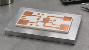
For the inverter, first name the insulation path: top copper to back copper or baseplate, or between two top-side copper islands. A test across one of these paths does not automatically cover the other. Record which electrodes are driven, returned, connected together or left open. For context on substrate construction, see the DBC ceramic substrate overview.
Partial Discharge Causes at the Copper Edge
Look for local field concentration and interfaces, not just ceramic thickness. Near a copper edge, metal, ceramic and a surrounding medium such as air or gel can meet at a triple junction. Edge shape, opposing copper layout and the surrounding dielectric can change the electric field there. Voids in encapsulation or defects elsewhere can produce similar electrical indications, so a report should distinguish suspected locations from confirmed ones.
A published study on DBC bottom copper examined how that layer affects discharge performance in power modules. Its implication for procurement is to compare the actual copper geometry and test configuration, not to copy an edge dimension or inception voltage into another drawing.
Partial Discharge vs Hipot
Ask for separate evidence when the specification requires both. A hipot or withstand test evaluates survival at the stated voltage and duration under its acceptance conditions. A charge-based PD test measures discharge-related pulses, typically reported as apparent charge, under its own conditions. The two methods can be combined in a defined program, but a simple withstand pass is not a PD result.
| Evidence | What it answers and what it does not |
| Withstand report | Did the sample meet the stated withstand criteria? It does not quantify PD unless the test also measured and reported it. |
| Charge-based PD report | What activity was detected at stated conditions? It does not establish unrestricted working voltage or service life. |
| Material dielectric strength | How did a material specimen perform under its breakdown method? It does not qualify the module’s edges, interfaces or encapsulation. |
Partial Discharge Measurement Unit: What Does pC Mean?
A picocoulomb (pC) is 10−12 coulomb. In a charge-based report it typically expresses apparent charge, a calibrated equivalent at the terminals, not the actual charge moved at an internal defect. Ask for the specified statistic, the measurement sensitivity, and the observed background under the stated test configuration.
A line that says “no PD detected” is only meaningful against a method, a voltage and a detection criterion. If the background prevents reliable discrimination at the agreed level, the result is inconclusive for that requirement, not a pass. A reading from a different sensor or method is not automatically interchangeable with a charge-based value.
Partial Discharge Inception and Extinction Voltage
Inception voltage (PDIV) identifies the voltage on the rising part of the agreed test sequence where activity meets the specified inception criterion. Extinction voltage (PDEV) refers to the falling part and the specified extinction criterion. Record how each was determined and whether the voltage is RMS, peak or DC. Neither value alone sets the continuous voltage rating.
For unit checking only, a 1.00 kV RMS sinusoid has a peak of approximately 1.41 kV because the peak is RMS × √2. That is not a suggested test level. The conversion does not make a sine-wave result comparable to a pulse or DC result, and it does not change the test object or its field distribution.
Partial Discharge Test Voltage: Match the Waveform and Object
Read the waveform and frequency before comparing values. IEC 60270:2025 covers charge-based measurements with AC up to 500 Hz or DC within its scope. IEC TS 61934:2024 addresses offline electrical measurements under repetitive impulses from power electronics; the two documents do not define interchangeable measurement methods.
The qualified lab and product requirements should determine the actual procedure, voltage sequence and limits. Do not improvise a high-voltage setup from a report. For the inverter, document whether the object was a bare coupon, metallized substrate or complete module and whether the result was measured before or after relevant conditioning. A bare sample tested in air does not include all of the interfaces found in a gel-filled module.

Partial Discharge Test Results: Separate Noise From Evidence
Ask what the lab did to separate discharge from the fixture, leads and external interference. A pattern may help form a hypothesis but does not by itself locate the defect. Have the lab document the background, calibration or sensitivity check appropriate to the method, and any repeats or reference measurements used to support the interpretation.
Do not reject the ceramic merely because one pulse appeared, and do not discard a repeatable signal as noise without a documented basis. If activity changes with fixture configuration rather than with the sample, investigate that difference before comparing lots. If the signal tracks a production geometry change across comparable samples, narrow the investigation to the relevant insulation path and confirm the result.
Partial Discharge Test Report: Decide What Is Fit for Release
Compare two reports only after the test object, insulation path, waveform and detection rules match the decision you need to make. For the inverter, request finished-module evidence when that is the specified acceptance object. Use the coupon data for material or process screening, with its limitations recorded.
| Report field | What to verify |
| Object and construction | Drawing revision, ceramic grade and thickness, copper geometry, and encapsulation state. |
| Insulation path | Electrode identities and any connection to the back copper or baseplate. |
| Exposure | Waveform, frequency or pulse definition, voltage units, sequence and conditioning. |
| Detection and decision | Method, calibration or sensitivity, background, result, applicable acceptance criterion and sample IDs. |
Hold the decision if the report cannot identify the production construction or cannot resolve the specified criterion above background. Agree on a repeat or a representative sample rather than adjusting a vendor result with a thickness ratio.
Frequently Asked Questions
Does a thicker ceramic always give a higher inception voltage?
No. Thickness changes one part of the field distribution. The edges, opposing metallization, surrounding dielectric and test connections can determine where activity starts. Compare production-intent geometries under the same method.
Can a larger copper setback replace a PD test?
No. A setback can change the local field and is worth reviewing, but a drawing dimension alone does not account for all interfaces, materials and process variation.
Is a low apparent-charge value proof that a void is small?
No. Apparent charge depends on how the discharge couples to the measurement terminals. Do not infer void dimensions from that value alone.
Can I compare DBC and AMB reports from different suppliers?
Only for decisions the evidence actually supports. Request comparable objects, electrode connections, conditioning, waveforms and acceptance criteria before attributing differences to the bonding process.
Does PD always lead immediately to breakdown?
No. Activity can occur without a complete conductive path at the time of the test. The potential effect on insulation depends on the materials, repetition and service conditions.
Can a PD report identify which lot a module came from?
Only if the test record links the sample ID to the relevant lot and drawing revision. A graph with no specimen identifier is not lot evidence.
Is there one pC limit for all ceramic substrates?
No. Use the product requirement and agreed test method. A threshold from a different type of equipment or sample is not a default limit for an inverter module.
When should I ask for a conditioned sample?
When the qualification plan requires evidence after a specified environmental or production exposure. Record the conditioning sequence and do not compare it directly with an unconditioned sample without noting the difference.
Prepare the Ceramic Substrate Review
For a Best Technology drawing and fabrication review, send the ceramic and copper stack, geometry, insulation paths and agreed evidence requirements to sales@bestpcbs.com. Confirm the scope of any requested test separately; a substrate fabrication review does not qualify the finished power module.