PCB manufacturing PCB manufacturing
Home > Blog

Decent Quality China SMT PCB Assembly Manufacturers

July 3rd, 2025

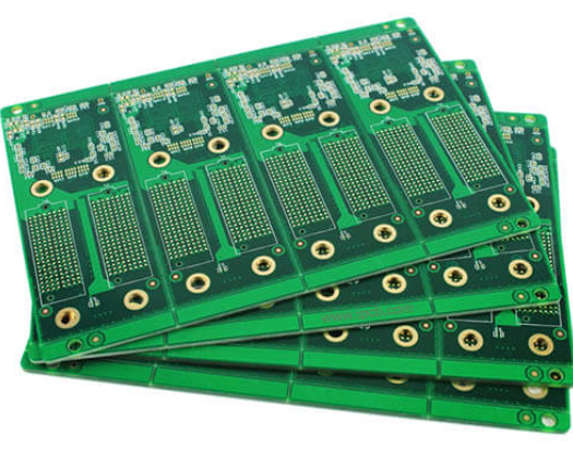
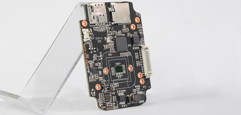
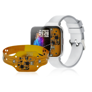
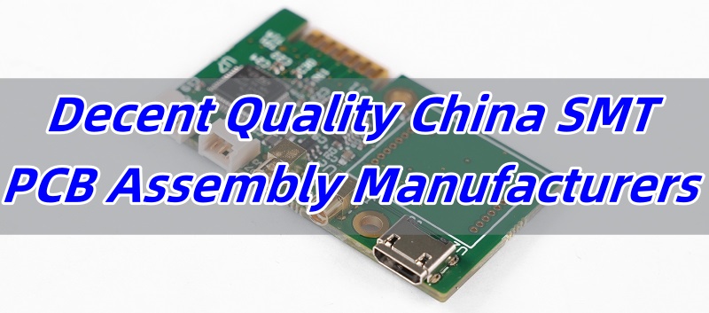
China SMT PCB assembly manufacturers are getting more attention from global buyers due to their rapid delivery, scalable production, and improved quality systems. As companies demand fast-turn, low-cost, and reliable assembly, it’s essential to understand how these manufacturers work and how to pick the right one.

EBest Circuit (Best Technology) is one of the well-established China SMT PCB assembly manufacturers. We take advantage of SMT technology and 19 years of experience to bring decent quality China SMT PCB assembly service to our prospects and regular customers. Most of our personnel in the R&D department and the sales department have over 10 years of experience in the PCBA industry. Decent quality, high mix, fast shipping, and no MOQ make us stand out head and shoulders above the competition. For any inquiries or requests to visit the factory, you can reach our engineers by email at sales@bestpcbs.com. 
Decent Quality China SMT PCB Assembly Manufacturers

Why Choose China SMT PCB Assembly Manufacturers for Your Projects?

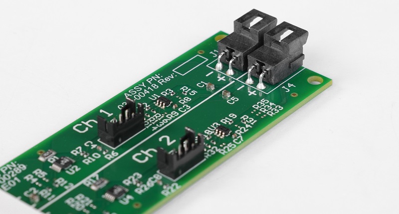
Chinese SMT assembly partners offer great value in terms of performance, efficiency, and price. Thanks to automation, MES systems, and digitalized quality controls, many Chinese factories now deliver boards with excellent solder quality and minimal defects. They’re especially known for balancing cost and speed without compromising on precision.

Another key reason is flexibility. Whether it’s a prototype or a mass production run, many factories in China can adjust fast. Their production planning is now backed by advanced system, making changeovers quicker and better managed. For businesses working with varied PCB designs, that agility is a big win.
Why Choose China SMT PCB Assembly Manufacturers for Your Projects?

Top 10 China SMT PCB Assembly Manufacturers List

When you’re sourcing reliable China SMT PCB assembly manufacturers, choosing a trusted name can save time, cost, and trouble. Many factories offer fast delivery and low prices, but only a few combine quality, process transparency, and strong customer support. Below are 10 manufacturers known for strong SMT capabilities, stable quality, and good communication with global clients.

1. EBest Circuit (Best Technology) Co., Ltd. – Shenzhen

EBest Circuit (Best Technology) focuses on high-mix, low-to-medium volume SMT and PCBA services. We also offer 24/7 technical support and advanced inspection systems to guarantee assembly quality.

2. Shenzhen Hitech Circuits Co., Ltd. – Shenzhen

Hitech Circuits provides one-stop solutions from PCB fabrication to SMT assembly. Their SMT lines are RoHS-compliant and equipped with AOI and X-ray inspection. They are known for quick delivery and stable quality for telecom and industrial sectors.

3. PCBCart – Hangzhou

PCBCart offers full-service PCB manufacturing and assembly, with fast prototyping and scalable production. Their SMT lines support both through-hole and mixed-technology builds. They also have a strong online interface for quote and tracking.

4. RayMing Technology – Shenzhen

RayMing is a mid-sized SMT service provider that handles both leaded and lead-free assembly. With IPC-A-610 trained operators and in-house engineering support, they provide detailed testing and full production documentation.

5. Screaming Circuits (China Division) – Suzhou

Although based in the U.S., Screaming Circuits collaborates with China-based facilities for assembly work. Their strength lies in prototype SMT builds with same-day or next-day delivery. They’re ideal for design engineers looking for fast turnarounds.

6. JLCPCB Assembly – Shenzhen

JLCPCB is one of the largest PCB manufacturers globally. Their SMT assembly division supports fully online orders and low-cost builds. They are best known for fast prototyping, although their service scope for customization is limited.

7. ALLPCB – Hangzhou

ALLPCB offers fast PCB production and assembly with instant online quotes. Their SMT services include stencil printing, pick-and-place, and reflow, combined with visual inspection. They’re suitable for small-to-medium runs.

8. MOKO Technology Ltd. – Shenzhen

MOKO provides turnkey PCB assembly, box build, and SMT testing services. With ISO13485, IATF16949, and UL certifications, they cater to medical, automotive, and industrial markets. Their DFM feedback helps reduce production errors early on.

9. Kingford PCB Assembly – Shenzhen

Kingford specializes in PCBA for consumer electronics and smart devices. They offer a strong parts sourcing network, competitive prices, and automated production lines. Their real-time feedback and engineering support are notable.

10. Shenzhen Sunsoar Tech Co., Ltd. – Shenzhen

Sunsoar Tech offers flexible SMT assembly services and supports low-volume custom orders. They’re known for personal service and offer a good balance between price and quality for startups and small businesses.

In summary, finding the right China SMT PCB assembly manufacturer depends on your needs. Some are great for prototypes. Others handle large runs with strict quality demands. The companies listed above are among the most dependable in China, with systems in place to ensure stable quality, fast delivery, and clear communication.

If you’re seeking a professional partner with complete quality traceability, flexible engineering support, and clear cost control—EBest Circuit (Best Technology) is a strong choice to start with.

What Makes Shenzhen PCB Manufacturers Stand Out Globally?

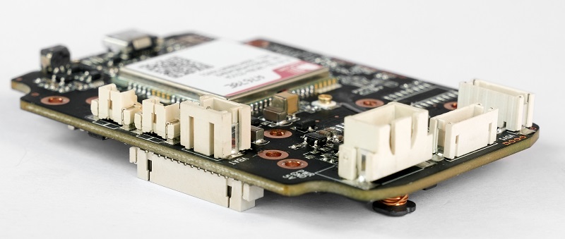
Shenzhen remains the core hub for PCB SMT China services. With thousands of component suppliers nearby, SMT houses in this area can secure parts faster and cheaper. Their logistics systems are integrated with sourcing platforms to avoid delays caused by shortages.

Also, the technical teams in Shenzhen factories tend to be more experienced. Many firms in this region offer remote diagnostic tools to assist clients after PCBA delivery. They also support DFM checks to help reduce defects before manufacturing begins.
What Makes Shenzhen PCB Manufacturers Stand Out Globally?

SMT Assembly Equipment Used by China PCBA Manufacturers

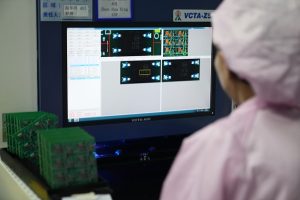
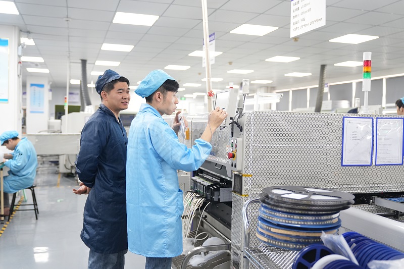
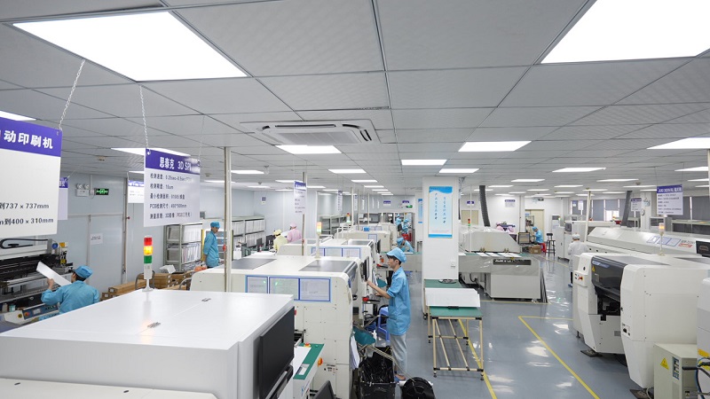
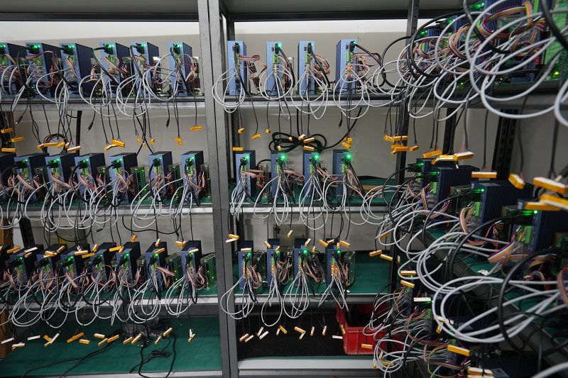
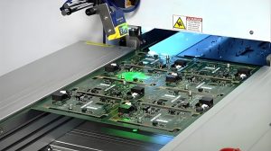
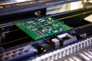
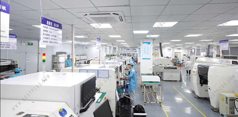
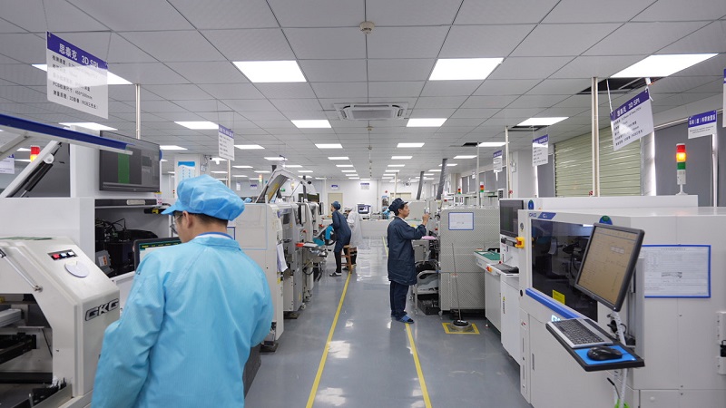
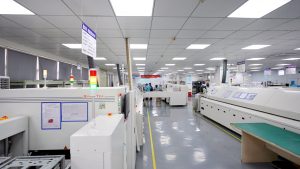
Advanced SMT assembly equipment plays a big role in final product quality. Today’s lines use 3D SPI machines to monitor solder paste thickness, and AOI to flag poor printing or component skew. These checks are automatic and fast, meaning issues can be caught early.

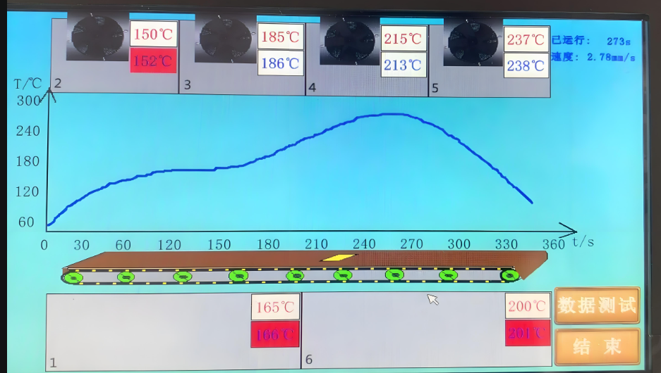
Reflow ovens are also getting smarter. With real-time temperature tracking, reflow curves stay stable, reducing the chance of under-soldering or bridging. Factories like EBest Circuit (Best Technology) upgrade regularly to maintain peak solder quality.

Equipment Name
High-Speed Placement Machine
Multifunctional Placement Machine
Nitrogen Reflow Oven
‌Nitrogen Generator
3D AOI
X-Ray
3D SPI
Smart First Article Tester
Automatic Solder Paste Printer

How to Select a Reliable SMT PCB Assembly Manufacturer in China?

Choosing the right partner takes more than comparing price quotes. Look for a manufacturer that provides real-time data, traceability, and fast engineering feedback. Transparency is key—especially in cost tracking and process control. Can they show the full process? Do they offer digital inspection reports?

Good manufacturers also provide strong communication. Cross-cultural gaps can cause delays. So teams that speak your language and understand your industry terms reduce risk. EBest Circuit (Best Technology), for instance, offers full English support and uses communication templates to keep everything clear and on track.

Why Choose EBest Circuit (Best Technology) as One of Your China SMT PCB Assembly Manufacturers?

  • EBest Circuit (Best Technology) addresses key industry problems with smart, customer-driven solutions. Our China SMT PCB assembly manufacturing systems are built around quality, visibility, and support. With a smart MES in place, our supply chain is linked in real-time, allowing faster component sourcing and reducing changeover times by up to 40%.
  • Plus, we use a transparent cost dashboard so customers can see where their budget is going. This builds trust and helps avoid future disputes.
  • Additionally, we offer high-mix PCBA services without MOQ, which include the assembly of PCBs, FPCs, ceramics, and MCPCBs. We cater to your SMT orders, whether they are large volume or small batch.
  • Finally, EBest Circuit (Best Technology) supports cultural alignment. Our team goes through culture sensitivity training and provides multi-language technical support. So even if you’re across the globe, collaboration stays smooth.
Why Choose EBest Circuit (Best Technology) as One of Your China SMT PCB Assembly Manufacturers?

In brief, China’s SMT industry is transforming. With tools like MES and lean production, the top players offer more than just fast service. They offer reliable partnerships. EBest Circuit (Best Technology) is one of them.

EBest Circuit (Best Technology)’s 19 years of experience with SMT PCB assembly service have been spectacular. We’ve tackled old problems like poor reflow quality, slow response, and cost confusion by investing in smart systems and clear communication. If you’re looking for a manufacturer that understands what global customers need—fast delivery, solid quality, and easy collaboration—then EBest Circuit (Best Technology) is the one to talk to. Interested in our PCBA? Drop us an email at sales@bestpcbs.com. 
You may also like

What is the Best Solder Temperature for PCB?

July 3rd, 2025

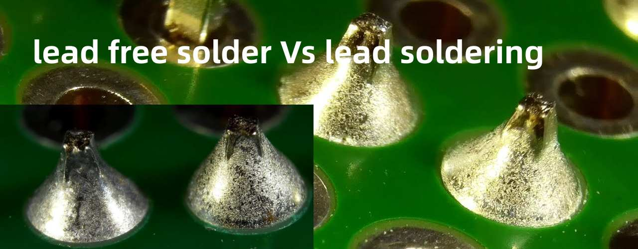
The typical solder temperature for PCBs is 240℃ to 270℃ for lead-free soldering, and 240℃to 260℃ for lead-based soldering.

If you’re building or repairing a PCB, knowing the right soldering temperature is key. It keeps your components safe and ensures strong connections. The temperature you use depends on the type of solder and the method. In this blog, we’ll break down everything you need to know about solder temperatures for PCBs.

What is the Best Solder Temperature for PCB?

Why Solder Temperature Matters in PCB Work?

When working with printed circuit boards, one of the most critical factors for quality and reliability is soldering temperature. Whether you’re assembling prototypes, repairing a PCB, or managing high-volume production, knowing the right temperature is essential for success.

Too low, and the solder won’t melt properly. Too high, and you might damage the board or components. Accurate temperature helps create reliable joints and avoids costly rework. It also protects sensitive parts from overheating.

Solder temperature affects not only how well the joints form but also how long your product will last in real-world use. In this blog, we’ll explore the ideal soldering temperatures for different solders and methods—and how to avoid costly mistakes.

What Determines Soldering Temperature?

Soldering temperature is not a fixed value. It depends on several key factors:

  • Type of solder alloy (leaded or lead-free)
  • Soldering process (manual, reflow, wave)
  • PCB material (standard FR-4, high-Tg, ceramic, etc.)
  • Component sensitivity
  • Ambient factory temperature and humidity

Each variable impacts how heat should be applied to the board. Applying the right temperature at the right time ensures the best wetting, strong mechanical bonds, and excellent electrical contact.

Solder Types and Their Melting Temperatures

  1. Lead-Based Solder (e.g., Sn63/Pb37)
  2. Melting point: 183°C
  3. Typical working temperature: 240°C to 260°C
  4. Benefits: Good wetting, lower processing temperature
  5. Drawbacks: Contains lead; banned in many consumer products (RoHS compliance)

Lead-based solder is often used in military, aerospace, or industrial environments where reliability outweighs regulatory restrictions. It’s easier to work with and provides strong joints with less thermal stress on components.

  • Lead-Free Solder (e.g., SAC305: Sn96.5/Ag3.0/Cu0.5)
  • Melting point: ~217°C
  • Typical working temperature: 245°C to 270°C
  • Benefits: RoHS compliant, eco-friendly
  • Drawbacks: Higher processing temperature, slightly brittle joints

Lead-free solder has become the standard in modern electronics manufacturing due to environmental regulations. However, it requires precise control of temperature and time to ensure quality results.

Solder Types and Their Melting Temperatures

Soldering Methods and Their Temperature Profiles

Let’s explore how soldering temperatures vary across different processes used in PCB manufacturing and assembly.

1. Reflow Soldering

Reflow soldering is the most common method for assembling surface-mount components. A solder paste (a mix of powdered solder and flux) is applied to the PCB, and components are placed on top. Then, the board goes through a reflow oven with controlled temperature zones.

Reflow Temperature Profile (Lead-Free):

  • Preheat: 150°C–180°C for 60–120 seconds
  • Soak: 180°C–200°C for 60–90 seconds
  • Reflow Peak: 240°C–250°C for 30–60 seconds
  • Cool-down: Controlled descent to room temperature

Reflow Temperature Profile (Lead-Based):

  • Preheat: 120°C–150°C
  • Soak: 150°C–180°C
  • Reflow Peak: 210°C–230°C
  • Cool-down: Gradual cooling to avoid thermal shock
Soldering Methods and Their Temperature Profiles

The peak temperature should not exceed the maximum rating of components, and the time above liquidus (TAL) must be kept short to avoid damaging the board.

2. Wave Soldering

Wave soldering is widely used for through-hole assemblies and some mixed-technology PCBs. The board passes over a wave of molten solder.

  • Lead-Based Solder: 245°C–255°C
  • Lead-Free Solder: 260°C–270°C

Before reaching the solder wave, the PCB is preheated to about 100°C–150°C to prevent thermal shock and improve solder wetting. Flux is applied before the preheat stage to clean and prepare pads.

3. Hand Soldering

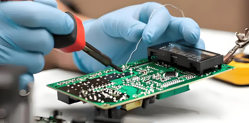
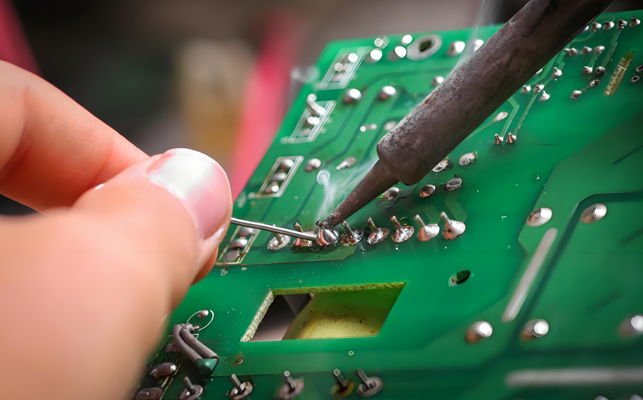
Hand soldering is still widely used in prototyping, repair work, or in low-volume custom assemblies. It uses a soldering iron with a temperature-controlled tip. Recommended tip temperatures:

  • Lead-Based Solder: 330°C to 370°C
  • Lead-Free Solder: 350°C to 400°C

While this may seem high, actual contact time is very short (1–3 seconds). A good soldering station will allow precise control and thermal recovery. Operators must avoid overheating pads or components.

Hand Soldering

Does the PCB Material Affect Soldering Temperature?

Yes—PCB material plays a major role in how much heat it can tolerate.

FR-4 (Standard)

  • Can handle up to 260°C for short durations
  • Common for most consumer and industrial PCBs

High-Tg FR-4

  • Higher glass transition temperature (Tg ~170°C to 180°C)
  • More stable under high thermal stress
  • Ideal for lead-free soldering or multilayer boards

Ceramic PCBs (Alumina, Aluminum Nitride)

  • Extremely high thermal stability
  • Can endure 300°C+ without damage
  • Requires more precise soldering to avoid cracking

Metal Core PCBs (Aluminum, Copper Core PCB)

  • Withstand up to 260°C for short durations
  • High thermal conductivity due to the metal core
  • Used in: Power electronics, lighting, and automotive control

Aluminum boards dissipate heat quickly, which helps during soldering. However, the uneven expansion between the metal and dielectric layer requires careful control to avoid mechanical stress during reflow.

Flex Circuits (Flexible PCBs)

  • Max soldering temperature: Typically <250°C
  • Material: Polyimide or PET base
  • Critical risk: Heat can distort, shrink, or damage traces

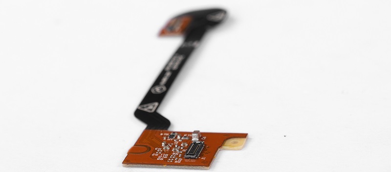
Flexible PCBs are more heat-sensitive than rigid boards. The polyimide or PET base can tolerate soldering but has lower thermal mass, which means it heats up—and cools down—faster. Excessive temperature or contact time can easily cause:

  • Wrinkling or warping
  • Delamination of copper traces
  • Tearing at bend areas

When soldering flex circuits:

  • Use lower reflow peak temperatures, typically not exceeding 240°C–245°C.
  • Apply thermal barriers or stiffeners in vulnerable areas.
  • Ensure the heating and cooling are gradual to prevent mechanical stress.

Flex PCBs often use selective soldering or low-temperature solders to reduce heat exposure. In some cases, hot-bar soldering or laser soldering is used for better temperature precision.

Common Soldering Issues Related to Temperature

IssueCausePrevention
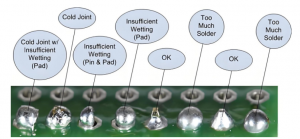
Cold jointsTemp too lowRaise temperature or improve heat transfer
Component damageTemp too high or too longShorten dwell time, use proper profiling
Solder bridgesExcess solder, poor controlUse precise stencil and paste volume
PCB delaminationOverheatingStay below board’s Tg and Td
Cracked jointsThermal shock during coolingUse controlled cooling stage

Why Choose EBest Circuit (Best Technology)’s PCB Soldering Service?

At EBest Circuit (Best Technology), we ensure every PCB assembly follows strict soldering standards. Our team uses professional thermal profiling tools to fine-tune the temperature curve for each product.

We support:

  • RoHS-compliant lead-free soldering
  • Lead-based solder for specialized industries
  • High-Tg and ceramic PCBs
  • Automated reflow and wave soldering
  • Manual soldering by IPC-trained operators

Suppose you have any questions about our products and service, price, MOQ, delivery, location, quality standards, certificates, engineering support and so on. We offer engineering support, thermal profiling, and high-quality PCB manufacturing for all your assembly needs. Please contact us freely any time. We aim to be the best PCB manufacturers in China to supply our customers with the best quality, price, and services. Contact us right now to discuss your next PCB project or to request a quote!

FAQs

1. What is the ideal soldering temperature for lead-free solder?

A peak reflow temperature of 245°C–250°C is typical. Manual soldering may require a tip temp of 350°C–370°C.

2. Can I use the same temperature for leaded and lead-free solder?

No. Lead-free solder needs a higher temperature due to its higher melting point.

3. Will high soldering temperatures damage my PCB?

If temperatures are too high or sustained too long, they can cause delamination, burnt pads, or component failure. Use proper profiling.

4. What’s the difference between peak temperature and tip temperature?

Peak temperature is the highest board temp during reflow. Tip temperature is the iron’s surface heat during manual soldering.

5. How can EBest Circuit (Best Technology) help with soldering specifications?

We provide detailed thermal profiles, component-safe soldering, and high-reliability assembly for all PCB types.

You may also like

Excellent Quality PCB PCBA China for Effective Delivery

July 3rd, 2025

PCB PCBA China is no longer just about low prices. Today, customers want stable supply chains, traceable production, and fast delivery—all backed by strong technical support. In this blog, we explore why EBest Circuit (Best Technology) is a trustworthy partner for your PCB and PCBA needs in China.

EBest Circuit (Best Technology) focuses on excellent quality PCB PCBA China for effective delivery. Both our factories in China and Vietnam have sophisticated SMT technology and engineers with lots of seniority. Most engineers have over 10 years of experience in the PCB industry and know how the PCBA process works. Strict inspection is performed in our factories, such as SPI, 3D AOI, X-Ray, and QC inspections. Low volume, high mix, consistent quality, and effective quality is our specialty. Welcome to chat with us over email at sales@bestpcbs.com about viable solutions and the specific quote for your project. 

Excellent Quality PCB PCBA China for Effective Delivery

Who is the Best Manufacturer of PCB PCBA China?

Among many PCB manufacturers in China, EBest Circuit (Best Technology) stands out with its advanced MES systems, flexible production scheduling, and industry certifications. With ISO 9001, IATF 16949, and AS9100D certifications, we meet strict quality standards required in automotive, medical, and aerospace sectors.

Who is the Best Manufacturer of PCB PCBA China?

What Are the Problems with PCB PCBA China?

Clients often face material shortages, delivery delays, and unstable quality. Many suppliers rely on manual systems for warehouse and quality control. This leads to missing components, inconsistent results, and long lead times. At EBest Circuit (Best Technology), we solve this by combining digital warehouse systems, JIT supply models, and automated testing lines to ensure real-time tracking and accurate results.

What is the Difference Between a PCB and a PCBA?

A PCB is the bare board, typically made of fiberglass or ceramic, with copper traces. PCBA is the complete assembly where components are soldered onto the PCB. In simple terms, PCB is the skeleton, while PCBA is the full body with all working parts in place. Understanding this helps you choose the right service level.

Are Motherboards Just PCBs?

Not exactly. While motherboards start as PCBs, they become PCBAs once fully assembled with CPUs, capacitors, connectors, and chips. This makes motherboards a finished electronic module, not just a printed board.

What Makes Chinese PCB Assembly Services Cost-Effective?

Chinese PCB assembly is cost-effective due to streamlined supply chains, shared infrastructure, and optimized labor. For example, EBest Circuit (Best Technology) reduces costs through BOM optimization engines that match substitute materials. We also use photovoltaic energy and waste heat recovery, cutting energy costs by 25%.

What Makes Chinese PCB Assembly Services Cost-Effective?

How to Choose a Reliable PCBA Manufacturer in China?

Look for key indicators: cleanroom production, certification coverage, transparent pricing, and a stable sourcing network. EBest Circuit (Best Technology) offers 72-hour agile delivery for urgent orders and real-time DFM checks through our customer portal. This helps reduce design flaws early and saves time and money.

Why Choose EBest Circuit (Best Technology) for PCB PCBA China?

We understand what matters to you—reliable delivery, consistent quality, and expert support. Our strengths include:

  1. Smart Warehousing: With MES integration and RFID, we track materials in real time and reduce supply delays.
  2. Automated Quality Control: AOI and X-Ray inspection ensure 99.5% defect detection. IoT-based monitoring fine-tunes soldering accuracy.
  3. Effective Delivery: A dual-supplier strategy, and three-month critical component coverage help us respond fast.
  4. Real-Time Support: Our engineers support 24/7 consultation service.  And our factory ‌production lines operate‌ round the clock.

Besides that, we don’t just offer a product; we provide long-term value. Our smart systems reduce downtime by 40%, and our DFM review boosts your product’s first-pass yield over 95%.

Why Choose EBest Circuit (Best Technology) for PCB PCBA China?

In brief, choosing a partner for PCB PCBA China is more than comparing prices. You need a supplier who prevents material shortages, keeps quality in check, and ships on time—every time. EBest Circuit (Best Technology) builds trust with its transparent process, cutting-edge systems, and customer-first approach. Whether you’re building medical devices or EV battery boards, our solutions are ready to help you grow. Let’s talk about how our expertise can speed up your project while keeping quality high. If you are interested in our efficient PCB assembly services, please contact us via email at sales@bestpcbs.com, on Twitter, or Facebook.

You may also like

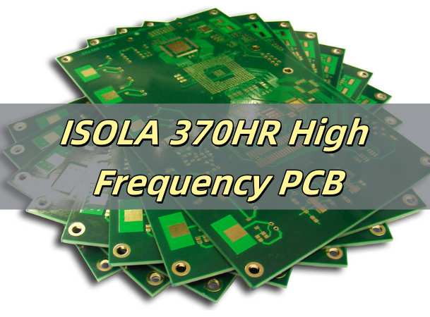
ISOLA 370HR High Frequency PCB

July 2nd, 2025

Isola 370HR is a well-established choice for engineers who need a durable, high-frequency compatible PCB base material. Its high Tg, low loss, and excellent reliability make it suitable for everything from aerospace to telecommunications.

If you’re working on a complex design or RF application, switching to Isola 370HR PCB materials might be the upgrade you need. And with a reliable partner like EBest Circuit (Best Technology), you’re assured of quality from the first prototype to volume production.

ISOLA 370HR High Frequency PCB

What Is Isola 370HR Material?

Isola 370HR is a high-performance, high-Tg epoxy laminate and prepreg system developed by Isola Group. Designed specifically for multilayer printed circuit boards, it offers a great balance between electrical stability and thermal durability. It’s classified as a high-Tg FR4 material but provides better signal handling and thermal behavior compared to standard FR4.

Isola engineered this material for demanding sectors like telecommunications, data networking, and military electronics. Its low dielectric loss and stable performance across a wide frequency range make it suitable for modern high-speed circuits.

Advantages of Using Isola 370HR in PCB Manufacturing

Choosing Isola 370HR for your PCB manufacturing brings several key benefits that directly impact the performance and reliability of your finished products:

  • Superior Thermal Stability: With a high glass transition temperature (~180°C), Isola 370HR withstands the high temperatures of lead-free soldering and multiple reflow cycles without warping or delamination.
  • Low Dielectric Loss: This material minimizes signal loss at high frequencies, making it perfect for RF circuits and high-speed digital designs.
  • Excellent Signal Integrity: Stable dielectric constant (Dk) across frequency ranges means consistent signal propagation and reduced timing errors.
  • Enhanced Moisture and CAF Resistance: Improved resistance to moisture-induced failures helps maintain long-term reliability, especially in humid or harsh environments.
  • Dimensional Stability: Reduced Z-axis expansion ensures layers stay aligned during manufacturing and operation, critical for multilayer PCBs.
  • IPC Compliance: Isola 370HR meets rigorous industry standards, ensuring compatibility with demanding aerospace, automotive, and medical applications.
  • RoHS and Environmental Compliance: Fully compliant with environmental regulations, supporting green manufacturing practices.
Advantages of Using Isola 370HR in PCB Manufacturing

ISOLA 370HR Datasheet

PropertyTypical ValueTest Method / Notes
Glass Transition Temperature (Tg)180°C (DSC)Differential Scanning Calorimetry
Decomposition Temperature (Td)>340°CTGA (Thermogravimetric Analysis)
Dielectric Constant (Dk)4.04 @ 1 GHzIPC-TM-650 2.5.5.5
Dissipation Factor (Df)0.0127 @ 1 GHzIPC-TM-650 2.5.5.5
Coefficient of Thermal Expansion (CTE)15 ppm/°C (X-Y), 65 ppm/°C (Z)IPC-TM-650 2.4.24
Thermal Conductivity0.4 W/m·KASTM E1461
Tensile Strength24,000 psiIPC-TM-650 2.4.18
Flexural Strength32,000 psiIPC-TM-650 2.4.4
Water Absorption<0.10%IPC-TM-650 2.6.2.1
Flammability RatingUL 94 V-0UL 94
Copper Peel Strength>1.0 lbs/inchIPC-TM-650 2.4.8
Surface Resistivity>1×10^6 ohmsASTM D257
Volume Resistivity>1×10^9 ohm-cmASTM D257
Dielectric Breakdown Voltage>50 kV/mmIPC-TM-650 2.5.6

What Is the Difference Between FR4 and 370HR?

While both standard FR4 and Isola 370HR are epoxy-based materials widely used in PCB manufacturing, they differ significantly in performance—especially when it comes to high-speed and high-frequency applications.

Standard FR4 is the go-to material for many general-purpose PCBs. It offers decent mechanical strength, good manufacturability, and cost-effectiveness for everyday electronics. However, its glass transition temperature (Tg) typically ranges from 130°C to 140°C, and it has relatively higher dielectric loss (Df). These limitations can cause signal degradation and reliability issues in circuits operating at higher frequencies or elevated temperatures.

In contrast, Isola 370HR is a high-Tg FR4 variant designed to meet the demands of more challenging environments. Its Tg is around 180°C, which provides superior thermal stability during lead-free soldering and extended use in high-temperature settings. More importantly, it exhibits a lower dielectric constant (Dk) and dissipation factor (Df), which translates to lower signal loss and better signal integrity at microwave and radio frequencies.

What Is the Difference Between FR4 and 370HR?

Why Isola 370HR PCBs Are Suitable for High Frequency Applications?

As electronic devices evolve to support faster data rates, the performance of PCB materials under high-frequency conditions has become a serious concern. This is where Isola 370HR PCB materials shine.

Its consistent dielectric constant (Dk) and low dissipation factor (Df) ensure that high-frequency signals do not lose strength or become distorted. That’s a major reason why 370HR is used in:

  • Gigabit Ethernet systems
  • High-speed backplanes
  • Automotive radar systems
  • Satellite communications
  • Advanced test equipment

Its ability to handle GHz-level signals without distortion helps maintain data accuracy and reduces EMI-related issues.

When to Choose Isola 370HR Material for Your PCB?

You might consider Isola 370HR when your design falls into any of the following categories:

High-speed or RF designs: If your circuit runs at over 1 GHz, this material can preserve signal quality.

  • Multilayer PCBs: When stacking 8 or more layers, 370HR offers great registration control and stability.
  • Thermal stress tolerance: It performs reliably through multiple reflow cycles and temperature extremes.
  • CAF-resistant needs: Ideal for products exposed to moisture or long-term outdoor use.
  • Strict industry compliance: It meets IPC-4101/126 and 129, as well as UL and RoHS requirements.

Choosing this material isn’t just about performance—it’s about peace of mind over the product’s lifecycle.

When to Choose Isola 370HR Material for Your PCB?

How to Identify Genuine Isola 370HR PCB Material?

To avoid counterfeit materials or unverified substitutions, it’s important to:

  • Request the original datasheet with the Isola logo and batch number.
  • Check board markings for Isola brand identification or laminate codes.
  • Work with certified suppliers who purchase directly from Isola or its authorized distributors.
  • Ask for certification documents, especially if your application is regulated by aerospace or medical standards.
  • Genuine Isola 370HR PCB materials ensure consistency in production and performance.

Typical Applications of Isola 370HR in PCB Design

Here are common industries and devices where Isola 370HR is frequently used:

  • Telecommunications: High-speed switches, routers, and fiber optic systems.
  • Aerospace and Defense: Radar, avionics, satellite boards.
  • Medical Equipment: Imaging devices, patient monitoring systems.
  • Automotive: Advanced driver-assistance systems (ADAS), LiDAR modules.
  • Industrial Automation: Motor controls, power management systems.

Designers across these sectors rely on its thermal reliability and signal control to reduce field failures.

What Is the Equivalent of Isola 370HR?

While Isola 370HR is a preferred material, there are other options that offer similar characteristics. Here’s how some alternatives compare:

Material NameTg (°C)Df @ 1GHzNotable Feature
Nelco N4000-13EP~180~0.013Known for stability
Panasonic MEGTRON 6~185~0.0025Ultra-low loss, but expensive
Ventec VT-47~180~0.014Cost-effective option

If you need better electrical performance than 370HR, MEGTRON 6 is a great choice. For general high-frequency use with cost control, 370HR remains the most balanced option.

Why Choose EBest Circuit (Best Technology) for Isola 370HR PCB Manufacturing?

With over 18 years of experience in printed circuit boards and as one of the leading PCB manufacturers, we support over 1,000 customers in different industrial areas worldwide. You can count on a PCB board manufacturer like us to meet your one-stop electronics manufacturing demands.

We are your one-stop PCB manufacturer in China who can meet all your diversified PCB requirements. We have an experienced engineering, production, and quality team that fully understands the unique needs of your industry—especially in medical, automotive, and aerospace applications. As a printed circuit board manufacturer, we always follow the most widely accepted standards in the industry: IPC-A-600 for fabrication and IPC-A-610 for PCB assembly. All our products meet IPC Class 2 by default, and we can also meet Class 3 or 3A when your application requires it.

If you have any questions about our products, services, pricing, lead times, quality control, certifications, or technical support, please feel free to contact us anytime. Our goal is to be one of the best PCB manufacturers in China, offering exceptional quality, fair pricing, and professional service.

FAQs

1. Is Isola 370HR good for RF applications?

Yes, it offers low dielectric loss and stable Dk, perfect for high-frequency circuits.

2. How is Isola 370HR different from standard FR4?

It has higher Tg, better thermal stability, and lower signal loss.

3. What industries use Isola 370HR PCB materials?

Telecom, automotive, aerospace, medical, and industrial electronics.

4. Can Isola 370HR support lead-free assembly?

Yes, it’s fully compatible with RoHS and lead-free soldering processes.

5. Where can I get a quote for Isola 370HR PCB fabrication?

Contact EBest Circuit (Best Technology) for fast, custom quotes and expert support.

You may also like

High Quality China PCBA PCB Assembly by Immediate Delivery

July 1st, 2025

China PCBA PCB assembly offers a fast, reliable solution for electronics manufacturing with high quality and immediate delivery. In this blog, we will show you the customer pain points, our competitive edges, PCBA PCB assembly capacities, qualification certifications, etc.
EBest Circuit (Best Technology) is a turnkey EMS PCB manufacturer offering high quality China PCBA PCB assembly by immediate delivery in world markets. We have 19 years of experience in the PCB & SMT PCBA industry. If you are interested in PCB assembly China, please contact us via our contact link here.

High Quality China PCBA PCB Assembly by Immediate Delivery

China PCBA PCB Assembly Pain Points from Customers

  • Quality Control Issues
  • Supply Chain Management
  • Soldering Process Challenges
  • Production Efficiency & Lead Time
  • Information & Data Management
  • After-sales Service Response
    CategorySpecific Issues
    1. Quality Control Issues– Component misalignment, soldering defects, open or short circuits at solder joints
    – Unstable raw material quality reduces overall product reliability
    – Manual operation errors lead to batch-level quality problems
    2. Supply Chain Management– Material shortages and delivery delays affect production schedules
    – Raw material price fluctuations make cost control difficult
    – Over-reliance on a single supplier creates supply chain vulnerability
    3. Soldering Process Challenges– High failure rate in BGA component soldering
    – Fine-pitch pads in high-density layouts are hard to solder
    – Inaccurate temperature control leads to thermal stress failures
    4. Production Efficiency & Lead Time– Traditional manufacturing methods are inefficient and slow
    – Manual paneling, dispensing, and other steps are time-consuming and error-prone
    – Lack of lean production mindset leads to wasted resources
    5. Information & Data Management– Complex production processes with poor traceability
    – Slow data collection makes real-time monitoring difficult
    – Troubleshooting takes time due to limited traceability
    6. After-sales Service Response– Long and complicated after-sales processes
    – Difficult to locate problems due to weak data tracking
    – Lack of a closed-loop system reduces problem resolution efficiency

    What can EBest Circuit (Best Technology) offer you?

    • Rigorous Moisture Control for Soldering Reliability
    • Advanced SMT Equipment and High Precision Printing & Placement
    • Comprehensive Quality Control and In-line Inspection Systems
    • Full Traceability and First Article Inspection for Every Project
    • Specialized Capabilities in Large Boards, Selective Soldering, and Conformal Coating
    • NO MOQ Requirement, Supporting Oder QTY from Large Volume to Small Batch
    • Immediate Delivery with a Lead Time of 1-5 days
    • 24/7 Rapid Responsiveness by Our Engineers and Account Representatives

    BEST Technology SMT PCB Assembly Capacities

    SMT Precision00105 components, 0.2mm pitch BGA, 0.25mm pitch connector
    SMT PCB SizeL50×50mm to L1200×360mm
    Assembly TypesSMD, Through Hole, Hand Soldering, Wire Assembly, DIP
    Testing CapabilitiesFunctional Test, ICT, X-RAY, AOI, SPI, IC Programming, Aging Test
    Box BuildingAssembly of enclosures including metal and plastic housings
    BEST Technology SMT PCB assembly Capacities:

    Quality and Certifications

    • Certified & Compliant Standards: ISO 9001, ISO 13485, IATF 16949, AS9100D Certified, and UL, REACH, RoHS Compliant
    • 100% Flying Probe Test – Verifies electrical connectivity for prototype or low-volume PCBs without needing a fixture.
    • 100% AOI (Automated Optical Inspection) – Full inspection of components and solder joints for placement accuracy, polarity, bridging, tombstoning, and missing parts.
    • X-RAY Alignment Inspection – Checks hidden solder joints (e.g., BGA, QFN) for misalignment, voids, and bridging.
    • Impedance Testing – Ensures controlled impedance traces meet design specifications, critical for high-speed signal transmission.
    • ICT (In-Circuit Test) – Detects manufacturing defects such as shorts, opens, component values, and soldering faults.
    • Functional Test (FCT) – Simulates real working conditions to verify the entire assembled board functions as intended.
    • SPI (Solder Paste Inspection) – Measures solder paste volume, height, area, and alignment before placement.
    • First Article Inspection (FAI) – Confirms all components are correctly placed and values are within tolerance before mass production.
    • Aging Test / Burn-in Test – Stresses the assembled boards under high temperature/load to identify early failures.
    • ESD Testing – Ensures boards are protected against electrostatic discharge during and after assembly.
    • Visual Inspection – Manual quality check for cosmetic and mechanical issues not easily captured by machines.
    • Continuity and Short Circuit Test – Verifies that there are no unwanted connections and all circuits are properly closed.

    Immediate Delivery

    • 1-5 days lead time
    • 24-hour shipping for urgent orders and time-critical projects
    • Quick turnaround for multilayer PCB prototypes and one-stop service from small-to-medium volume PCBA
    Immediate Delivery

    Applicable Industries for SMT PCB

    • Consumer Electronics – Smartphones, tablets, smartwatches, cameras, and home appliances
    • Automotive Electronics – ADAS, lighting systems, infotainment units, ECU, and battery management systems
    • Medical Devices – Patient monitors, diagnostic equipment, infusion pumps, and wearable health tech
    • Industrial Automation – PLCs, sensors, controllers, and industrial power supplies
    • Telecommunications – Routers, base stations, network switches, and optical modules
    • Aerospace & Defense – Radar systems, navigation modules, avionics, and mission-critical controls
    • LED Lighting – LED drivers, street lights, automotive lighting, and smart lighting systems
    • IoT & Smart Devices – Smart home products, tracking devices, and wireless communication modules
    • Renewable Energy – Solar inverters, battery storage systems, and power controllers
    • Computing & Storage – Servers, SSDs, memory modules, and data processing boards
    Applicable Industries for SMT PCB

    FAQs

      • Q: What is the minimum stencil thickness you can make?
        A: 0.06mm, 0.08mm, 0.10mm, 0.12mm.
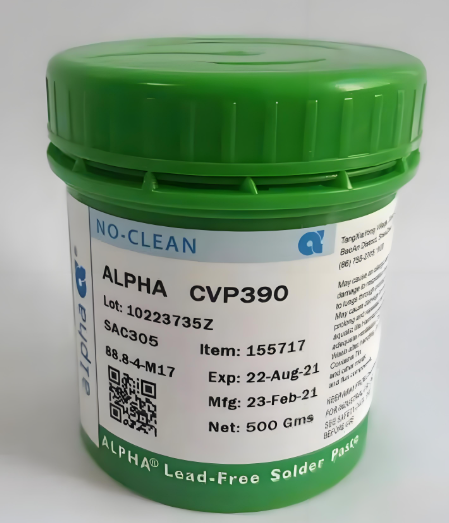
      • Q: What is the recommended warming time, mixing time, and storage temperature for solder paste?
        A: The solder paste should be warmed to room temperature for about 4 hours before use. It needs to be mixed or stirred thoroughly for approximately 3 minutes to ensure uniform consistency. For storage, the solder paste should be kept refrigerated at a temperature between 2°C and 10°C to maintain its quality and shelf life.

      Instant Quote

      China PCBA PCB assembly is your trusted solution for high quality, fast turnaround, and reliable manufacturing to meet urgent project demands. If you have any further questions or would like to discuss the details of your project, please call us at +86-755-2909-1601 or email us at sales@bestpcbs.com. You can also chat with us through our online customer service option located on the right side of the Contact Us page.
          You may also like

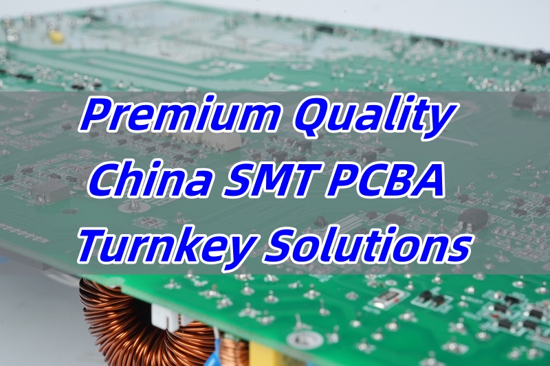
          Premium Quality China SMT PCBA Turnkey Solutions

          June 30th, 2025

          China SMT PCBA is the first choice for many global brands when they need speed, flexibility, and quality all in one package. In recent years, more companies have switched to turnkey services to cut costs and reduce lead time. But not all suppliers are equal. That’s why understanding what makes a solution truly premium is key to making the right decision.

          EBest Circuit (Best Technology) offers premium quality China SMT PCBA turnkey solutions in the global market. Our customer orders can be ‌routed flexibly‌ through our ‌SMT facilities in China or Vietnam, subject to ‌technical requirements‌ and ‌trade considerations‌. The advanced equipment, comprehensive process control, and intelligent manufacturing capabilities give us a competitive edge over the average competitors. ‌Our SMT factories are equipped with state-of-the-art equipment, including high-speed chip mounters from Panasonic, as well as SMT PCBA machines from YAMAHA and JUKI. We also utilize advanced inspection tools, such as 3D AOI, X-ray machines, and 3D SPI. Feel free to send us an e-mail at sales@bestpcbs.com for turnkey SMT PCBA solutions.

          Premium Quality China SMT PCBA Turnkey Solutions

          What Services Are Included in a China SMT PCBA Turnkey Solution?

          A full turnkey service means more than just soldering components. It covers the entire journey—component sourcing, PCB fabrication, SMT and DIP assembly, testing, packaging, and even delivery. Some providers also assist with design verification or offer DFM checks early in the process to prevent future issues. With a reliable partner, you get all services from a single source, reducing delays and miscommunication.

          What Services Are Included in a China SMT PCBA Turnkey Solution?

          Who Is the Best Manufacturer of China SMT PCBA?

          The best partner is one who delivers quality consistently and solves customer demands. EBest Circuit (Best Technology) stands out for its combination of advanced MES systems, certified quality management (ISO 9001, ISO 13485, IATF 16949, AS9100D), and real-time material tracking. It’s not just about making boards. It’s about helping customers reduce their defect rate, stay on schedule, and get traceable production data.

          Who Is the Largest China SMT PCBA Manufacturer?

          While there are large players like Foxconn or BYD that serve big OEMs, mid-size companies often need faster responses and more flexibility. That’s where EBest Circuit (Best Technology) shines. With factories in both Shenzhen and Dongguan, and dedicated engineering teams, Best offers tailored PCBA services without the high MOQs and long queues seen at large OEM suppliers.

          Who Is the Largest China SMT PCBA Manufacturer?

          How Does PCBA in China Compare to Other Regions in Terms of Cost and Quality?

          China provides a unique mix of cost advantage and technical depth. While countries like Vietnam offer lower wages, they often lack strong supply chains and technical support. In contrast, China SMT PCBA manufacturers like EBest Circuit (Best Technology) combine automation, quality control, and skilled labor, which drives down rework rates and total cost over the project lifecycle.

          How to Evaluate the Quality of a China SMT PCBA Manufacturer?

          Start with certifications. Look for ISO, IATF, or medical-grade credentials. Then dig deeper. Do they use SPI, AOI, ICT, and X-ray inspection? Can they provide traceable data for every step? At EBest Circuit (Best Technology), full process control and material tracking are standard. Our MES system gives real-time visibility into material use, which helps solve problems like stock errors or replenishment delays.

          How to Evaluate the Quality of a China SMT PCBA Manufacturer?

          What Should You Check Before Choosing a China SMT PCBA Manufacturer?

          Check these points:

          • Do they have in-house PCB fabrication or rely on outsourcing?
          • Is their SMT line modern and well-maintained?
          • Do they provide DFM or DFx reviews?
          • Can they handle small batch orders and scale when needed?
          • Do they support after-sales engineering and rework?

          EBest Circuit (Best Technology) not only ticks all the above boxes but also helps manage unexpected changes. Whether it’s last-minute part replacements or urgent lead time adjustments, we respond fast with flexible production plans.

          Why Choose EBest Circuit (Best Technology) for China SMT PCBA?

          Here’s why so many brands rely on us:

          • ERP + MES Integration: We solve warehouse and stock visibility issues by using ERP and MES systems. No more line-side material delays.
          • Intelligent Production: Our SMT lines include inline SPI, AOI, and X-ray checks, reducing solder defects like cold joints, shorts, or bridging.
          • Responsive Team: Fast DFM feedback, rapid quote turnaround, and 24/7 engineering support make project launch smoother.
          • Custom-Tailored Support: We help you find the balance between cost and quality, even with complex or high-mix builds.
          Why Choose EBest Circuit (Best Technology) for China SMT PCBA?

          To sum up, choosing the right China SMT PCBA partner is more than finding the lowest price. It’s about trust, responsiveness, and being ready to handle complexity. EBest Circuit (Best Technology) doesn’t just assemble boards. We help solve deeper challenges—like poor stock management, unclear traceability, inconsistent soldering, and late deliveries.

          With our strong process control, real-time systems, and highly responsive team, we help you reduce risk, speed up delivery, and improve product reliability. If you’re looking for a long-term PCBA partner who understands real manufacturing needs, we’re ready to help. Please feel free to e-mail us directly at sales@bestpcbs.com for a viable solution for China SMT PCBA.

          You may also like

          Extraordinary Quality China PCBA for Efficient Delivery

          June 30th, 2025

          China PCBA solutions are changing how electronics manufacturers think about speed, quality, and reliability. In this blog, we’ll explore how EBest Circuit (Best Technology) delivers professional SMT PCBA manufacturing, driven by cutting-edge systems and a commitment to excellence.

          EBest Circuit (Best Technology) is a leading PCB & PCBA Manufacturer offering extraordinary quality China PCBA for efficient delivery. We place a priority on innovation and have a professional research and development department that has been creating patents annually, thanks to our seasoned talents. EBest Circuit (Best Technology) promotes team spirit and provides quick responsiveness service to both our prospects and regular customers. We implement shift work at our SMT PCBA factories in China & Vietnam, where the on-time delivery rate is up to 97%. Both factories are ISO 9001, ISO 13485, IATF 16949, and AS9100D compliant. Rest assured that we can effectively handle both large and small-volume orders. Feel free to contact us at sales@bestpcbs.com for any technical inquiries or requests to make a factory visit. We are happy to give our full engagement and show you around our factory at your convenience.

          Extraordinary Quality China PCBA for Efficient Delivery

          What is the best China PCBA company?

          The best China PCBA company combines speed, quality, and dependability. EBest Circuit (Best Technology) is a standout in the industry. We use full-process digital quality control to reach nearly perfect production efficiency. Our first-pass yield exceeds 99.9%, thanks to precise control and minimal human error. We also offer a stable lead time of 7 days, meeting the demand of fast-moving industries without sacrificing quality. Our customer satisfaction rate reaches 98%, a result of responsive technical support and after-sales service.

          What is the best China PCBA company?

          Who is the best China PCBA supplier?

          EBest Circuit (Best Technology) is recognized as a leading China PCBA supplier. We serve global markets with robust PCBA services including design, sourcing, assembly, and testing. With certifications like ISO 13485, AS9100D, and IATF 16949, we meet the standards required for medical, aerospace, and automotive industries. Our systems trace each PCB with a unique ID, speeding up issue tracking by 90%. We also deploy AOI, SPI, and X-ray inspection for a 99.97% defect capture rate.

          Who is the largest China PCBA manufacturer?

          China has many large PCBA manufacturers, each with strengths in different sectors. Below are three major players:

          1. Shenzhen Kaifa Technology: Known for large-scale EMS, they serve telecom and consumer electronics. They focus on smart manufacturing and rapid delivery.
          2. Huaqiang Electronics: A major supplier in the China PCB market. They offer complete solutions from design to PCBA assembly, including sourcing and testing.
          3. BYD Electronics: Originally an automotive company, they now provide PCBA services across industries, offering strong R&D and automated lines.

          These companies provide large-scale services, but many customers prefer more responsive and flexible partners like EBest Circuit (Best Technology). With lean production lines and quick delivery, we give more attention to individual projects.

          Who is the largest China PCBA manufacturer?

          What is the difference between a PCB and a PCBA?

          The key term here is PCBA vs PCB. A PCB (Printed Circuit Board) is the blank board with copper traces. A PCBA (Printed Circuit Board Assembly) includes all mounted components like resistors, chips, and connectors. So, PCBA is a complete working circuit. We not only produce PCBs but also handle sourcing, assembly, and testing to deliver complete PCBA products ready for integration.

          What are the problems with PCBA?

          Every manufacturer faces challenges. Here’s a breakdown of common PCBA issues and their impacts:

          ProblemImpact
          Unstable qualityHigh defect rate reduces reliability
          Soldering issues (cold joints, voids, etc.)Account for over 60% of total defects
          No traceability78% of companies cannot locate root causes, leading to long rework time
          Manual inspection dependencyYield rate fluctuates over 15%
          Uncontrolled delivery schedulesComponent lead time causes 65% of delays
          Frequent reworkCauses 3–5 days of delivery delay
          Cost vs quality conflictTrying to cut costs may raise defect rates

          EBest Circuit (Best Technology) addresses all these problems with digital inspection, predictive maintenance, and robust logistics support.

          How expensive is China PCBA?

          The cost of China PCBA depends on complexity, parts, and order size. However, EBest Circuit (Best Technology) balances price and quality well. We apply lean production, centralized sourcing, and predictive logistics to cut unnecessary costs. Our long-term vendor relationships help us get better prices, which we pass on to our clients.

          Is BEST in China?

          Yes, EBest Circuit (Best Technology) is based in China. We operate a modern facility equipped with advanced SMT lines, X-ray, AOI, SPI, and MES systems. We serve both domestic and global clients with end-to-end PCBA services. Our location in Shenzhen offers fast access to electronic components and efficient shipping options.

          Why choose EBest Circuit (Best Technology) for China PCBA?

          We go beyond manufacturing. Here’s why customers choose us:

          • Stable quality: Achieved through full-process digital control and triple inspection systems.
          • Fast delivery: 7-day lead time with intelligent supply chain and emergency line setup.
          • High reliability: Our defect rate stays below 0.1%, even for complex builds.
          • Component sourcing: Over 500 supplier partners and predictive stock ensure parts availability.
          • Responsive support: 24/7 technical help with direct engineer contact, reducing wait time.
          • Customization: Flexible solutions for medical, automotive, LED, and other specialized applications.

          Our system offers not just production but a total solution. From fast prototyping to volume orders, we keep communication simple and outcomes consistent. When other suppliers struggle with delays or defects, we bring stability and precision.

          Why choose EBest Circuit (Best Technology) for China PCBA?

          To wrap up, China PCBA services are efficient, but not all manufacturers deliver the same results. Thorough supplier vetting is vital to maintain consistent quality standards. EBest Circuit (Best Technology) provides viable solutions to customers—from digital traceability to fast delivery and high reliability. We shorten delivery times by 53% and improve quality by over 70%. If you’re looking for dependable PCBA manufacturing in China, EBest Circuit (Best Technology) is your next move. Just feel free to let us know your specific SMT PCBA requirements via sales@bestpcbs.com.
          You may also like

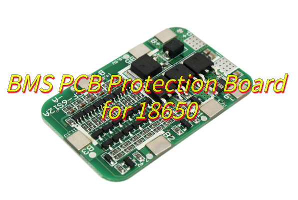
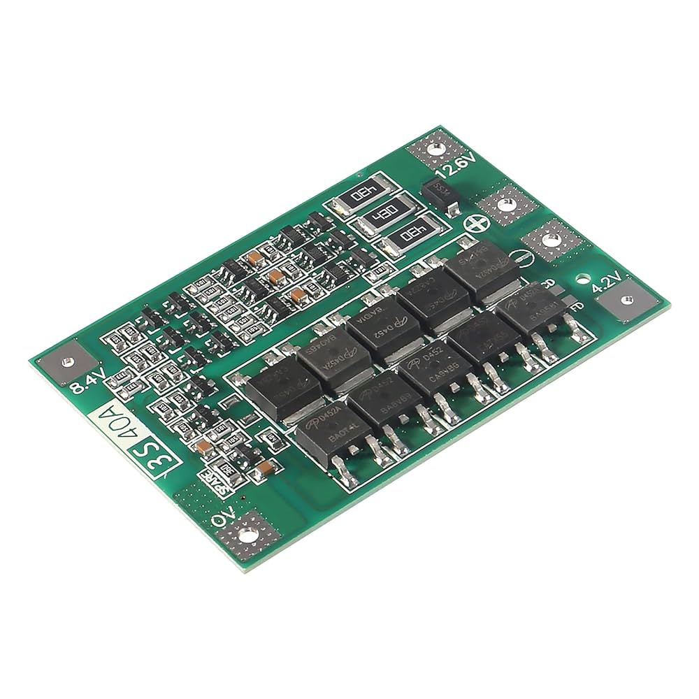
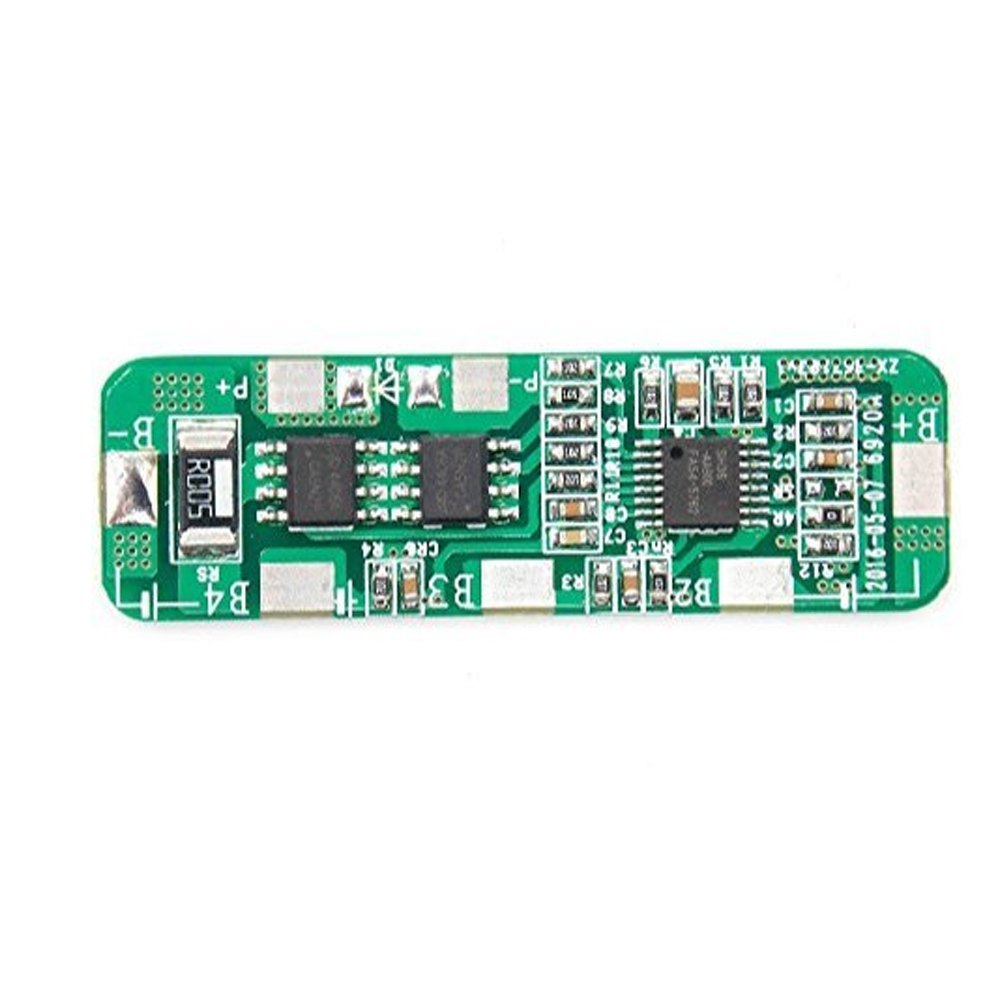
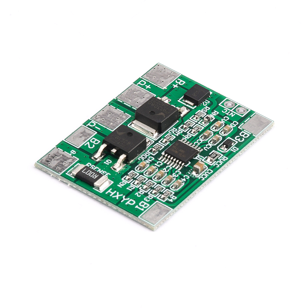
          BMS PCB Protection Board for 18650​

          June 30th, 2025

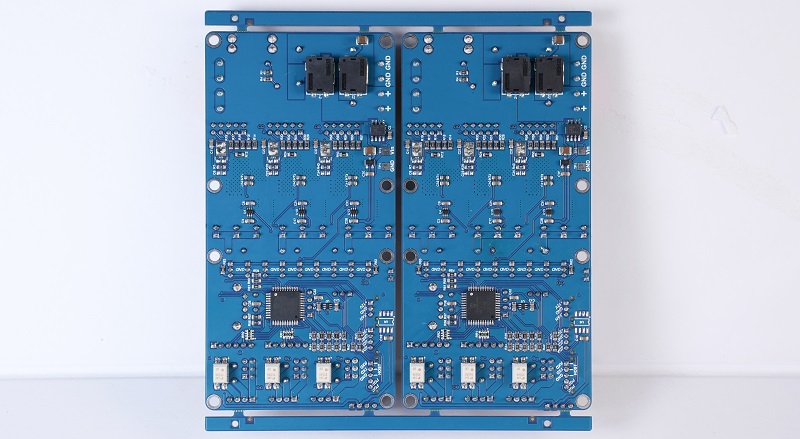
          How BMS PCB keeps your 18650 battery pack safe and efficient?‌ This guide covers everything from wiring and design to cost-effective noise shielding and heat management for optimal BMS PCB protection.

          Using 18 years of BMS PCBA technology accumulation, we will protect your battery safety!

          • Poor welding? – Nitrogen reflow + 3D SPI detection to eliminate false welding
          • Delivery delay? – Intelligent scheduling system guarantees 7-day delivery
          • Cost out of control? – Standardized process reduces 15% assembly cost
          • Poor compatibility? – Support TI/ADI/NXP and other multi-platform solution adaptation

          EBest Circuit (Best Technology) Provide:

          • Integrated solution – From PCB design to finished product assembly, BMS protection board “plug and play” is realized
          • High-precision mounting – 01005 component mounting accuracy ±25ÎŒm, ensuring the stability of the sampling circuit
          • Triple test guarantee – AOI+ICT+FCT full inspection, fault interception rate increased to 99.97%
          • Flexible production – Support 1-16 layer board mixed production, 24-48 hours ultra-fast prototyping.

          Let every BMS PCB become the intelligent guardian of the battery system! Contact us now: sales@bestpcbs.com.

          What Is BMS PCB?

          A BMS PCB (Battery Management System Printed Circuit Board) serves as the central control unit for rechargeable battery packs, ensuring safe and efficient operation. It monitors vital parameters including individual cell voltages, overall current flow, and temperature distribution across connected battery cells. When detecting potentially hazardous conditions such as overcharging, excessive discharge, or abnormal heat buildup, the system automatically disconnects the battery through integrated protection circuits to prevent permanent damage.

          To maintain consistent performance, most BMS PCBs incorporate cell balancing functionality, which adjusts charge distribution among cells during operation. This process helps maximize available energy storage while extending battery lifespan. Communication capabilities allow the board to relay operational data, including state-of-charge estimates and system warnings, to connected devices through standard interfaces. The implementation varies across applications, with simpler versions managing small consumer electronics and more advanced configurations supporting high-capacity systems like electric vehicles and renewable energy storage installations.

          What Is BMS PCB?

          How to Wire PCB BMS?

          Here’s a practical guide to wiring a BMS PCB, focusing on achieving reliability, safety, and performance:

          1. Establish Accurate Cell Voltage Monitoring

          • Connect each cell voltage sense wire directly to its corresponding cell terminal within the battery pack. Keep these sense wires as short and consistent in length as feasible and route them away from high-current paths to minimize noise interference and ensure precise voltage readings by the BMS PCB.

              2. Implement Dedicated High-Current Paths

              • Use appropriately thick traces or busbars for the main battery pack positive (P+) and negative (P-) connections entering the BMS PCB. Similarly, size the discharge (B-) and charge/discharge output (C- or P-) traces adequately to safely carry their maximum expected currents without excessive voltage drop or heating.

              3. Apply Effective Grounding Strategies

              • Create a solid, low-impedance reference ground plane on the BMS PCB near the current shunt resistor. Physically separate and connect sensitive analog measurement grounds (like cell sense circuits) directly to this reference point before connecting noisy digital grounds or high-current FET grounds.

              4. Route Signal Traces Mindfully

              • Physically separate sensitive signals like cell voltage sense lines. Shield communication lines (CAN, UART, etc.) whenever possible using twisted pairs, shielded cables, or ground planes adjacent to the traces on the BMS PCB itself.

              5. Install Thermistors Securely

              • Mount temperature sensors directly onto the cell surface or module terminals where thermal monitoring is required. Route their connecting wires carefully to avoid snagging or damage and connect them securely to the designated thermistor input pins on the BMS PCB.

              6. Connect Balancing Components Efficiently

              • Link balancing resistors or FETs directly to their respective cell sense points. Ensure the balancing current paths on the BMS PCB have adequate trace width for the balancing current level without causing localized heating. Tightly group balancing components to shorten signal paths.

              7. Select and Wire Suitable Connectors

              • Choose connectors rated well above the maximum operating current and voltage, with sufficient pin density and locking mechanisms. Match wire gauges to current loads. Clearly label all connector positions for unambiguous wiring to the BMS PCB.

              8. Integrate Protective Elements

              • Install necessary fuses or circuit breakers in series with the main pack positive (P+) input path before it reaches the BMS PCB. Ensure the fuse rating aligns with system capabilities. Connect any external contactor control coils to the designated driver outputs on the BMS PCB.

              9. Verify Connections Thoroughly

              • Before applying power, meticulously check all wiring against the BMS PCB schematic and layout diagram. Use a multimeter to confirm absence of short circuits, verify correct voltage polarity at each sense point, and ensure thermistor resistances read correctly at the connector.

              How to Design BMS PCB Heat Dissipation Structure to Avoid MOSFET Hot Spot Failure?

              Here are practical approaches to design BMS PCB heat dissipation structures that effectively prevent MOSFET hot spot failures:

              • Strategic Component Placement: Position MOSFETs away from other heat-generating components and near board edges or ventilation areas. Allow sufficient spacing between devices to enable airflow and prevent thermal interference.
              • Optimized Copper Pour Layout: Use thick copper layers (≄2 oz) for power traces and create large, continuous copper areas connected to MOSFET source/drain pins. Expand these pours to maximize surface area for heat dissipation.
              • Thermal Via Implementation: Place dense arrays of thermal vias beneath MOSFET packages, connecting top-side heat sources to inner copper layers or bottom-side heatsinks. Follow manufacturer recommendations for via diameter and spacing.
              • Effective Heatsink Integration: Design PCB mounting points for clip-on or screw-attached heatsinks. Ensure flat surface areas under MOSFETs for proper thermal interface material contact when using external cooling solutions.
              • Current Distribution Balancing: Implement symmetrical layouts with identical trace lengths when using parallel MOSFETs. This prevents uneven current sharing that could cause localized overheating in individual devices.
              • Thermal Relief Pad Design: Configure solder pads with appropriate thermal relief patterns – enough to allow proper soldering while maintaining efficient heat transfer to the PCB copper.
              • Temperature Monitoring Integration: Embed temperature sensors near expected hot spots, positioned to detect actual MOSFET case temperatures rather than ambient board temperature for accurate thermal management.
              How to Design BMS PCB Heat Dissipation Structure to Avoid MOSFET Hot Spot Failure?

              How to Shield BMS PCBs from High-Voltage Noise Without Breaking the Budget?

              Cost-effective strategies to shield BMS PCBs from high-voltage noise

              Prioritize TVS Diodes for Transient Voltage Suppression

              • Implementation: Install TVS diodes at power inputs and critical signal lines (e.g., CAN bus, sensor interfaces).
              • Why: Clamps high-voltage spikes from load dumps or inductive switching, diverting excess energy to ground.
              • Cost Efficiency: Low-cost unidirectional/bidirectional TVS arrays (e.g., SMAJ series) provide robust protection without complex circuitry.

              Optimize PCB Layout for Noise Isolation

              • Ground Plane Strategy: Use dedicated ground layers for analog/digital sections. Separate high-current paths (e.g., battery cell balancing) from low-voltage sensor traces.
              • Trace Routing: Keep high-voltage traces >2mm from sensitive signals. Avoid 90-degree bends to minimize impedance discontinuities.
              • Decoupling: Place 0.1”F ceramic capacitors near every IC power pin and 10”F electrolytic capacitors at PCB entry points.

              Leverage Ferrite Beads for HF Attenuation

              • Application: Insert ferrite beads (e.g., Murata BLM series) in series with power lines to the MCU and communication modules.
              • Benefit: Dissipates high-frequency noise as heat without affecting DC power delivery.
              • Budget Tip: Use multi-layer chip inductors (e.g., 1206 size) for cost-effective EMI filtering.

              DIY Shielding with Copper Tape or Aluminum Enclosures

              • Low-Cost Enclosure: Line BMS housing with adhesive copper foil (≀$5 for 1mÂČ) and connect to PCB ground.
              • Gap Management: Seal seams with conductive gasket tape to prevent electromagnetic leakage.
              • Alternative: Repurpose aluminum tooling plates as shields, secured with nylon screws to avoid ground loops.

              Software Filtering for Noisy Sensors

              • Algorithm: Implement a moving average or Kalman filter in BMS firmware to smooth voltage/current readings.
              • Example: Apply a 10-sample moving average to cell voltage data to reject transient spikes from motor noise.
              • Zero Hardware Cost: Leverage unused MCU flash memory to store filter coefficients.

              Isolation Techniques for Critical Nodes

              • Optocouplers: Use low-cost optoisolators (e.g., PC817) for relay drivers or charge enable signals.
              • Digital Isolators: For CAN/RS-485 interfaces, adopt cost-effective isolators like ISO7741 (under $2 in qty).
              • Galvanic Separation: Prevent ground loops by isolating high-voltage sampling circuits from the main MCU.

              What Is A BMS Protection PCB Board?

              A BMS protection PCB board is a dedicated hardware solution designed to ensure battery pack safety by monitoring critical parameters in real time. This printed circuit board tracks cell voltages, pack current, and temperature distribution while comparing these values against predefined safety thresholds. When detecting unsafe conditions like overvoltage, undervoltage, excessive current, or high temperatures, it activates protective measures through control elements such as power MOSFETs to isolate the battery. The board also incorporates cell balancing functions, state-of-charge estimation, and communication interfaces to relay system status. Its primary purpose is to provide autonomous hardware-level protection that prevents catastrophic failures while maintaining safe battery operation.

              What Is A BMS Protection PCB Board?

              How to Use PCB BMS Protection Board for 18650s?

              How to use a PCB BMS protection board for 18650 batteries:

              1. Inspect the BMS and Batteries

              • Confirm the BMS matches your 18650 cell count (e.g., 4S for four 3.7V cells in series).
              • Check battery voltage with a multimeter to ensure no cell is below 2.5V before connecting the BMS.

              2. Wire the Battery Pack

              • Connect the battery pack’s negative terminal to the BMS B- port using 16–20 AWG silicon wire.
              • Route each cell’s balance wire (B1+, B2+, etc.) to the corresponding BMS balance ports. Avoid crossing wires to prevent short circuits.

              3. Connect Charger and Load

              • Attach the charger’s negative lead to the BMS P- port and positive lead to the battery pack’s positive terminal.
              • Connect the load (e.g., device, inverter) to the same P- port and pack positive, ensuring the load’s current draw does not exceed the BMS rating.

              4. Secure and Ventilate the BMS

              • Mount the BMS using nylon standoffs to prevent contact with metallic surfaces.
              • Ensure adequate airflow around the BMS, especially if it lacks built-in heat sinks.

              5. Initial Power-Up and Testing

              • Charge the pack at 0.5A–1A initially to verify the BMS triggers overcharge protection at 4.25V per cell.
              • Discharge the pack with a low-power load (e.g., LED light) to test over-discharge cutoff at 2.5V per cell.

              6. Balance Cells Regularly

              • After 3–5 cycles, use a battery analyzer to check cell voltages. Manually discharge any cell exceeding 4.2V using a resistor.
              • Avoid full discharges to minimize voltage imbalance between cells.

              7. Monitor Temperature and Connections

              • Check for overheating near MOSFETs during high-current use. Reduce charge/discharge current if temperatures exceed 60°C.
              • Tighten terminals monthly to prevent loose connections, which can cause erratic behavior.

              8. Replace Aging Components

              • Inspect capacitors for bulging every 12 months. Replace if signs of leakage or swelling appear.
              • Upgrade to a BMS with higher current ratings if using the pack for high-drain applications (e.g., e-bikes).

              How to Choose PCB BMS Protection Board for 18650?

              Match Cell Count and Voltage

              • Choose a BMS that supports your battery pack’s configuration (e.g., 4S for four 3.7V cells in series).
              • Verify the BMS’s maximum voltage rating exceeds your pack’s fully charged voltage (e.g., 16.8V for a 4S pack).

              Check Current Ratings

              • Select a BMS with a continuous discharge current rating 20% higher than your application’s peak demand (e.g., 30A BMS for a 25A e-bike motor).
              • Ensure the charge current rating aligns with your charger’s output (e.g., 5A BMS for a 4A charger).

              Evaluate Protection Features

              • Prioritize boards with overcharge, over-discharge, over-current, and short-circuit protection.
              • Look for optional features like cell balancing, temperature sensors, and low-voltage recovery modes.

              Inspect Physical Design

              • Choose a BMS with labeled terminals and spaced-out ports to simplify wiring.
              • Prioritize models with integrated NTC thermistor ports for precise temperature monitoring.

              Verify Communication Protocols

              • For smart packs, ensure the BMS supports your device’s protocol (e.g., I2C, SMBus) or includes Bluetooth/Wi-Fi for remote monitoring.
              • Test compatibility with your charger or energy meter before finalizing.

              Review User Feedback

              • Check forums or reviews for reports of false triggers, uneven balancing, or premature MOSFET failures.
              • Avoid boards with frequent complaints about solder joint quality or inaccurate voltage readings.

              Balance Cost and Longevity

              • Avoid ultra-cheap BMS units with thin traces or generic MOSFETs, as they may fail under stress.
              • Invest in models with replaceable fuses or upgradeable firmware for future-proofing.
              How to Choose PCB BMS Protection Board for 18650?

              How to Balance Cost and Stability of BMS PCB Protection Board for 18650​?

              Here are actionable tips to balance cost and stability when selecting a PCB BMS protection board for 18650 batteries:

              Prioritize Essential Protections Over Premium Add-Ons

              • Ensure the PCB BMS protection board includes core features: overcharge, over-discharge, over-current, and short-circuit protection. These are non-negotiable for safety.
              • Avoid paying extra for advanced functions like Bluetooth monitoring or active cell balancing unless your application requires them.

              Evaluate Component Quality Carefully

              • Check for MOSFETs with mid-range current ratings (e.g., 40V/60A vs. 80A+). They offer sufficient durability for most 18650 packs without inflating costs.
              • Look for ceramic capacitors instead of electrolytic ones for better temperature stability and longer lifespan.

              Balance Current Ratings with Real-World Needs

              • Choose a PCB BMS protection board with a continuous discharge rating 10–20% above your system’s maximum draw (e.g., 25A BMS for a 20A tool). This avoids over-engineering costs.
              • Avoid boards rated far beyond your requirements, as higher current tolerance often increases price disproportionately.

              Leverage Passive Cell Balancing

              • Opt for PCB BMS protection boards with passive balancing (resistor-based) instead of active balancing (inductor-based). Passive designs are cheaper and sufficient for most 18650 applications.
              • Ensure the balancing current is ≄50mA to maintain cell health over hundreds of cycles.

              Inspect Trace Width and PCB Thickness

              • Choose a board with 2oz copper traces and a minimum thickness of 1.6mm. These specs reduce resistance and heat buildup without adding significant cost.
              • Avoid ultra-thin PCBs (e.g., 0.8mm), as they may warp or delaminate under stress.

              Check for Replaceable Fuses or Resettable PTCs

              • Some PCB BMS protection boards include user-replaceable fuses or polymer PTCs (resettable breakers). These features extend the board’s lifespan by allowing recovery from overcurrent events.
              • Compare costs: A board with a $0.50 PTC may outlast three cheaper boards without this feature.

              Review Open-Source Firmware Options

              • Select a PCB BMS protection board with publicly available firmware (e.g., via GitHub). This lets you customize protections or fix bugs without relying on the manufacturer.
              • Community-supported boards often have lower long-term maintenance costs due to shared troubleshooting resources.

              Conclusion

              In conclusion, this guide has comprehensively covered the essential aspects of BMS PCB protection boards for 18650 battery systems, from fundamental concepts to practical wiring techniques, thermal management solutions, and cost-effective noise shielding approaches. We’ve explored proper usage methods, selection criteria, and the critical balance between performance and affordability. For reliable battery management systems that prioritize both safety and efficiency, these components prove indispensable. Should you require high-quality BMS PCB solutions tailored to your specific 18650 applications, we recommend contacting EBest Circuit (Best Technology) for professional consultation and competitive pricing. Their expertise ensures optimal battery protection while meeting your technical and budgetary requirements. Welcome to contact us: sales@bestpcbs.com.
              You may also like

              Super Quality PCBA Manufacturer in China for Fast Delivery

              June 27th, 2025

              PCBA Manufacturer in China is a keyword that resonates with global buyers who demand fast, precise, and trusted electronics assembly services. If you’re looking for a reliable partner who delivers consistent quality on tight timelines, you’re not alone. The competition in electronics manufacturing is intense, and choosing the right PCBA supplier is no longer just about cost—it’s about control, speed, and support.

              To ensure every customer enjoys super quality PCBA and satisfactory service, EBest Circuit (Best Technology) offers DFA checks, rapid prototyping service, and a wide range of PCBA choices for customers, such as 4L, 6L, 8L, and 12L FR4 PCB assembly, 4L rigid-flex PCBA assembly, ceramic PCB assembly, and box building services. EBest Circuit (Best Technology) is a PCBA board manufacturer for electronics in China. We promise a super-quality SMT PCBA and efficient delivery. And we will provide the best service for you. Feel free to share your BOM list, silk screen position diagram, and SMD coordinates with us at sales@bestpcbs.com, and we will be pleased to share our specific quoting correspondingly.

              Super Quality PCBA Manufacturer in China for Fast Delivery

              Who Is the Best PCBA Manufacturer in China?

              Many companies call themselves top suppliers, but the best PCBA manufacturer in China goes beyond high volume. It’s about who can provide stable quality, quick turnaround, and full technical backup. EBest Circuit (Best Technology), for example, has earned the trust of global clients through a well-managed MES system, certified production (ISO9001, ISO13485, IATF16949, AS9100D), and a customer-first approach. Clients choose them not just for products—but for comprehensive solutions.

              Who Is the Best PCBA Manufacturer in China?

              Where Are Most PCBA Manufactured?

              Most PCBA manufacturing in China is concentrated in regions like Shenzhen, Dongguan, and Suzhou. Shenzhen stands out as the heart of the electronics industry. With access to a robust supply chain, skilled labor, and modern logistics, PCBA China suppliers in this area offer faster prototyping and flexible batch production. That’s why many global electronics brands choose this hub for their key projects.

              What Services Do Top PCB Assembly Manufacturers in China Offer?

              Leading PCBA board manufacturers for electronics in China don’t just offer assembly. They provide full turnkey services—PCB fabrication, SMT, DIP soldering, functional testing, BGA rework, and conformal coating. EBest Circuit (Best Technology) adds an extra layer of value through DFM feedback, component suggestions, and custom packaging. In-house AOI, X-ray, ICT, and full traceability reporting help buyers avoid quality risks and shorten development cycles.

              What Services Do Top PCB Assembly Manufacturers in China Offer?

              What Is the Difference Between Bare PCB and PCBA?

              The terms sound similar but represent two different stages. A bare PCB is the raw board with only copper traces and no parts. A PCBA (Printed Circuit Board Assembly) includes all the soldered components. The jump from PCB to PCBA adds complexity and responsibility—especially in terms of inspection, process control, and final test. So, working with a skilled PCBA China team can reduce rework, returns, and missed deadlines.

              Who Is the Manufacturer of Bare PCB in China?

              China has countless PCB manufacturers. However, very few manage both bare board production and complete PCBA in one location. EBest Circuit (Best Technology) is one of the few that offers integrated services. This helps maintain consistency between PCB and assembly quality. No more back-and-forth between multiple suppliers. Customers benefit from a single point of accountability, stronger material control, and fewer delays.

              Who Is the Manufacturer of Bare PCB in China?

              How to Choose a Reliable Shenzhen PCBA Manufacturer for Fast Turnaround?

              First, check for certifications—ISO 9001, ISO 13485, IATF 16949, and others prove the factory follows international standards. Second, examine their testing process. Do they use AOI, X-ray, ICT, and FCT? Third, review their past delivery records. Finally, talk to their support team. A fast response today shows how they’ll support you tomorrow. EBest Circuit (Best Technology) checks all the boxes and adds extra value with proactive DFM support and 24/7 communication. Fast delivery isn’t luck—it’s planning.

              How to Choose a Reliable Shenzhen PCBA Manufacturer for Fast Turnaround?

              Why Choose EBest Circuit (Best Technology) for PCB & PCBA Manufacturer in China?

              Customers choose EBest Circuit (Best Technology) for a reason. Their strength lies in four pillars:

              • Quality Control: They operate under a complete quality system—from raw material inspection to final test. Every board passes AOI and functional checks before shipping.
              • Fast Delivery: Thanks to lean manufacturing and automated lines, urgent orders ship in as fast as 24–48 hours.
              • Technical Support: Their engineering team works with your design to avoid issues before production starts.
              • Customer Service: Around-the-clock response ensures you’re never left waiting.

              Moreover, EBest Circuit (Best Technology) manages orders with a clear process and always seeks continuous improvement. Whether you’re scaling up or launching a new design, they reduce your risks and help you move fast—without quality trade-offs.

              Why Choose EBest Circuit (Best Technology) for PCB & PCBA Manufacturer in China?

              As a final point, finding the right PCBA Manufacturer in China is more than a search—it’s a strategic decision. Customers today need more than just low cost. They want accountability, speed, quality, and clear communication. EBest Circuit (Best Technology) stands out with its strong engineering, fast delivery, rigorous testing, and transparent support model. In a world where missed deadlines and poor quality hurt business, choosing a trusted partner like EBest Circuit (Best Technology) can make a big difference for your projects.

              EBest Circuit (Best Technology) is a super quality PCBA manufacturer in China for fast delivery. If you’re tired of delays, rework, and poor communication, it’s time to work with a supplier who delivers not just boards—but viable solutions. Please email EBest Circuit (Best Technology) at sales@bestpcbs.com if you have new inquiries or would like to schedule a factory visit with us.

              You may also like

              Embedded Boards Prototyping & Assembly, Fast Turnaround

              June 25th, 2025

              Seeking for embedded boards solutions for your project? This guide explores their definition, components, types, and practical solutions for prototyping, thermal management, and cost optimization, helping you navigate efficient embedded development.

              EBest Circuit (Best Technology) specializes in high-speed embedded board prototyping and assembly with guaranteed 24-hour turnaround time, backed by 18 years of industry experience serving 500+ clients annually. Our manufacturing capabilities cover advanced HDI (up to 20 layers), impedance control (±5% tolerance), and thermal management solutions, all produced in ISO 9001-certified facilities with <0.3% defect rates. Transparent pricing structure delivers 15-25% cost savings compared to industry averages, as verified by third-party audits. Testimonials from automotive and medical device clients confirm 30% faster time-to-market using our services. Contact our engineering team today for a no-obligation quote and experience prototype-to-production excellence: sales@bestpcbs.com.
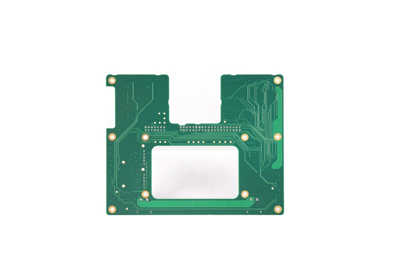
              What Is An Embedded Board?

              An embedded board is a dedicated computing platform designed to perform specific functions within a larger system. Unlike general-purpose computers, it integrates a processing unit (like a microcontroller or microprocessor), memory, input/output interfaces, and power regulation into a single compact circuit board. These boards operate autonomously with specialized firmware, enabling precise control in applications ranging from medical devices to industrial automation.

              This inherent specialization demands rigorous prototyping and precise assembly. Rapid turnaround becomes valuable during development, allowing engineers to test functionality, optimize thermal performance, and validate real-world reliability before full-scale production. Efficient prototyping ensures the final embedded board delivers consistent operation under its intended environmental constraints.

              What Is An Embedded Board?

              What Are Components of Embedded Boards?

              Components of embedded boards:

              Microcontroller/Microprocessor

              • The “brain” of the embedded board, this chip executes code and manages tasks. Common options include ARM Cortex-M series for low-power devices or ESP32 for Wi-Fi/Bluetooth-enabled boards.

              Memory (RAM and Flash)

              • RAM: Temporary storage for running programs (e.g., 512MB DDR3 for real-time data processing).
              • Flash: Permanent storage for firmware (e.g., 16MB NOR flash for code storage).

              Power Management Circuitry

              • Includes voltage regulators (to convert 5V/12V inputs to 3.3V logic) and power-on-reset chips to stabilize operation during voltage fluctuations.

              Input/Output (I/O) Interfaces

              • GPIO Pins: For connecting buttons, LEDs, or sensors.
              • Serial Ports: UART for debugging, SPI/I2C for peripherals like displays or EEPROM.

              Communication Modules

              • Wired: Ethernet PHY, CAN bus for industrial machines.
              • Wireless: Wi-Fi 5/6, Bluetooth 5.0, or LoRa for IoT connectivity.

              Sensors and Actuators

              • Sensors: Temperature (e.g., LM35), motion (MPU6050), or light (BH1750) interfaces.
              • Actuators: Motor drivers (L298N) or relay controls for automation.

              Clocks and Timers
              Real-time clocks (RTC) with battery backups for timestamping, and precision timers for PWM signal generation (e.g., 1kHz motor control).

              Protection Components

              • ESD Diodes: Guard against static discharge (e.g., 8kV rating).
              • Fuses: Resettable PTC fuses for overcurrent protection.

              What Are Types of Embedded PCB Boards?

              Types of embedded boards:

              • Microcontroller Boards‌: These boards incorporate a microcontroller unit (MCU) with integrated memory and peripherals, making them suitable for basic input/output operations and real-time control in embedded settings, such as home automation or sensor monitoring.
              • Single-Board Computers (SBCs)‌: Compact boards that function as complete computing systems, featuring processors, memory, and interfaces, often employed for more demanding tasks in embedded projects like multimedia processing or networking.
              • System-on-Module (SoM) Boards‌: Modular designs that package core computing elements onto a small board, intended for easy integration into larger custom systems, commonly used in scalable embedded solutions for wearables or robotics.
              • Development Boards‌: Purpose-built for prototyping and testing, these boards include accessible pins, sensors, and debugging tools to facilitate experimentation and learning in embedded design environments.
              • Evaluation Boards‌: Designed to assess the capabilities of specific components or chips, these boards help developers evaluate performance and compatibility before finalizing embedded system implementations.
              • FPGA Boards‌: Utilizing Field-Programmable Gate Arrays, these boards allow for customizable hardware logic, enabling adaptable processing for specialized embedded applications like signal routing or real-time control.
              • DSP Boards‌: Focused on digital signal processing capabilities, these boards excel in handling audio, video, or other signal-intensive tasks within embedded systems, such as in communication or medical devices.

              Why Choose Embedded Boards Prototyping?

              Here are reasons why choose embedded board prototyping:

              • Early Functionality Testing‌ – Prototyping allows verification of core features before full production, ensuring the embedded board performs as intended.
              • Design Validation‌ – Helps identify and fix hardware and software issues early, reducing costly revisions later.
              • Performance Optimization‌ – Enables real-world testing of power consumption, signal integrity, and thermal behavior for refinement.
              • Cost Efficiency‌ – Catching flaws early prevents expensive manufacturing errors and reduces overall development expenses.
              • Faster Time-to-Market‌ – Accelerates development by allowing quick iterations and validation before mass production.
              • Customization Flexibility‌ – Facilitates adjustments for specific needs, such as adding or removing peripherals based on test results.
              • Integration Testing‌ – Verifies compatibility with other system components, ensuring smooth operation in the final product.
              • Risk Reduction‌ – Minimizes unexpected failures by validating real-world performance under different conditions.
              • Iterative Development‌ – Supports gradual improvements based on feedback, leading to a more reliable final embedded board.

              How to Optimize Embedded Single Board Computer Prototyping Design to Reduce Costs?

              Below are measures to optimize embedded single board computer prototyping design for cost reduction:

              Leverage Highly Integrated System-on-Chip (SoC) Solutions

              • Select SoCs with built-in peripherals (e.g., Wi-Fi, Bluetooth, GPU) to minimize external components. This reduces board complexity, lowers bill-of-materials (BOM) costs, and simplifies assembly.
              • Prioritize SoCs with long-term availability to avoid redesign costs due to component obsolescence.

              Adopt Open-Source Hardware and Software Frameworks

              • Utilize reference designs from open-source communities (e.g., Raspberry Pi Compute Module, BeagleBone) to accelerate development and reduce engineering hours.
              • Use free or low-cost development tools (e.g., Arduino IDE, PlatformIO) and open-source libraries (e.g., FreeRTOS, Linux kernels) to eliminate licensing fees.

              Optimize Power Management Design

              • Incorporate low-power modes (e.g., sleep, hibernate) and dynamic voltage scaling to extend battery life or reduce energy consumption in always-on applications.
              • Use efficient power regulators (e.g., switching regulators instead of linear ones) and optimize PCB layout to minimize power loss.

              Standardize Connectivity and Interfaces

              • Use universal connectors (e.g., USB-C, HDMI) and industry-standard protocols (e.g., I2C, SPI) to avoid custom cables or adapters, reducing procurement and inventory costs.
              • Design for compatibility with existing peripherals (e.g., sensors, displays) to leverage economies of scale and reduce integration risks.

              Implement Design-for-Manufacturability (DFM) Principles

              • Simplify PCB layout by reducing layer counts and via densities. Use automated design rule checks (DRC) to identify cost drivers (e.g., tight tolerances, non-standard materials).
              • Collaborate with contract manufacturers early to optimize component placement and assembly processes, avoiding costly rework.

              Prioritize Component Reuse and Scalability

              • Develop modular architectures where core functionalities (e.g., processing, memory) are separated from application-specific modules (e.g., I/O boards). This allows reuse across projects and delays customization to later stages.
              • Use socketed components (e.g., memory modules) instead of soldered parts to enable easy upgrades and repairs, extending product lifespan and reducing waste.
              How to Optimize Embedded Single Board Computer Prototyping Design to Reduce Costs?

              How to Accelerate Prototyping Cycles for Custom Embedded Development Boards?

              Practical measures to accelerate prototyping cycles for custom embedded development boards:

              Adopt Modular Hardware Architecture

              • Break the system into reusable functional blocks (e.g., processing, power, I/O) with standardized interfaces. This enables parallel development of subsystems and reduces dependency on full assembly for testing.
              • Use off-the-shelf carrier boards or adapter modules for core functions (e.g., processors, wireless modules) to defer customization until later stages.

              Leverage Rapid Prototyping Platforms

              • Utilize development kits with compatible pinouts or form factors (e.g., Arduino shields, Pmod modules) to validate core logic before finalizing custom PCB designs.
              • Repurpose open-source hardware schematics and layouts as starting points to skip low-level design tasks.

              Implement Virtual Prototyping and Simulation

              • Use circuit simulators to test analog/digital designs and power integrity before fabricating PCBs.
              • Employ firmware-in-the-loop (FIL) testing to debug software interactions with simulated hardware peripherals.

              Prioritize Agile Firmware Development

              • Develop firmware incrementally using test-driven design (TDD) principles. Start with minimal viable features and expand functionality in sprints.
              • Use abstraction layers for hardware interfaces to decouple firmware from hardware revisions, enabling parallel software/hardware refinement.

              Streamline PCB Fabrication and Assembly

              • Partner with quick-turn PCB manufacturers offering 24–48 hour prototyping services and automated optical inspection (AOI).
              • Use panelized designs to combine multiple board revisions in a single panel, reducing setup costs and enabling side-by-side comparisons.

              Automate Testing and Validation

              • Build automated test jigs using microcontrollers or programmable logic devices (PLDs) to run regression tests on every prototype iteration.
              • Integrate logging and diagnostics into firmware to capture failure modes during real-world testing, minimizing manual debugging time.

              Collaborate with Component Suppliers Early

              • Engage distributors or manufacturers during the design phase to secure samples of critical components (e.g., sensors, connectors) and validate part availability.
              • Use supplier-provided reference designs or application notes to accelerate layout and compliance testing (e.g., EMC, thermal).
              How to Accelerate Prototyping Cycles for Custom Embedded Development Boards?

              How to Fix Overheating Issues in High Power Embedded Control Boards Assembly?

              Measures to resolve thermal management issues in high-power embedded control boards assembly:

              Strategically Position High-Power Components

              • Action: Place heat-generating components (e.g., MOSFETs, inductors) near PCB edges or align them with ventilation slots. Avoid clustering them in central regions.
              • Tool: Use free thermal simulation tools like KiCad Thermal Relief or SolidWorks Flow Simulation to model airflow and identify hotspots.
              • Outcome: Reduces heat accumulation in critical areas by 30–50%.

              Upgrade to High-Performance Thermal Interface Materials (TIMs)

              • Material: Replace generic thermal pads with Gelid GP-Extreme (15 W/mK) or Fujipoly XR-e (9 W/mK) for component-to-heatsink connections.
              • Tip: Apply a 0.1mm layer of Arctic MX-6 thermal paste using a plastic card to ensure even coverage without air gaps.
              • Outcome: Lowers junction-to-case thermal resistance by 20–40%.

              Design Custom Aluminum Heat Sinks with Fin Optimization

              • Action: Machine heat sinks from 6063 aluminum alloy with 15–20mm fins spaced 2–3mm apart for natural convection. For forced airflow, use 5–10mm fins spaced 1–2mm apart.
              • Tool: Use HeatSinkCalculator.com to optimize fin dimensions based on airflow velocity.
              • Outcome: Improves heat dissipation by up to 60% compared to stock designs.

              Integrate Low-Noise Active Cooling

              • Solution: Install Sunon MagLev 40mm x 10mm fans (25 dB noise rating) with PWM control to target hotspots. For extreme cases, use Corsair Hydro X micro-reservoirs with distilled water cooling.
              • Tip: Mount fans 10–15mm above the board to avoid vibration transfer.
              • Outcome: Reduces peak component temperatures by 15–25°C under full load.

              Maximize PCB Thermal Conductivity

              • Design: Fill inner layers with 2–3mil thermal vias in a staggered grid pattern beneath hot components. Use 2 oz/ftÂČ copper for power planes and 1 oz/ftÂČ for signal layers.
              • Material: Specify Isola FR408HR laminate (Tg 180°C) for better high-temperature stability.
              • Outcome: Spreads heat 40% more efficiently across the PCB.

              Select Components with Integrated Thermal Safeguards

              • Parts: Use Infineon OptiMOS™ power MOSFETs (with built-in temperature sensing) or Texas Instruments TPS546D24A PMICs (with thermal shutdown).
              • Action: Configure thermal alerts via I2C to trigger automatic power throttling (e.g., reduce CPU frequency by 20% at 90°C).
              • Outcome: Prevents thermal runaway while maintaining system functionality.

              Validate with Accelerated Thermal Testing

              • Test: Run 72-hour burn-in tests at 120% of rated power using Chroma 63600 load banks. Monitor temperatures with MAX31875 I2C sensors logged every 10 seconds.
              • Tool: Use FLIR E5 thermal camera to visualize heat spread during testing.
              • Outcome: Identifies marginal designs early, avoiding costly field failures.

              How to Prevent Warping in High-Density Embedded Circuit Board Assemblies?

              Below are methods about how to prevent warping in high-density embedded circuit board assemblies:

              Use Low-CTE Laminate Materials

              • Select PCB substrates with a coefficient of thermal expansion (CTE) matching copper (e.g., 17–20 ppm/°C) to minimize differential expansion during soldering.
              • Prioritize high-Tg (glass transition temperature) laminates (e.g., 170°C+) to resist deformation under prolonged thermal exposure.

              Implement Symmetrical Layer Stack-Up

              • Design the PCB with balanced copper distribution across layers (e.g., equal signal/power planes on top and bottom). Asymmetric copper weights cause uneven stress.
              • Avoid placing heavy copper features (e.g., large ground planes) on one side without compensation on the opposite layer.

              Optimize Component Placement for Stress Relief

              • Space large components (e.g., BGAs, connectors) evenly to prevent localized stress concentrations. Use stitching vias around high-mass parts to anchor them during thermal cycling.
              • Avoid clustering tall components (e.g., electrolytic capacitors) near board edges, which act as leverage points for warping.

              Control Reflow Soldering Profiles

              • Use a gradual ramp-up rate (1–2°C/second) in the reflow oven to allow gradual thermal expansion. Avoid abrupt temperature spikes.
              • Extend the soak zone (150–180°C) by 30–60 seconds to preheat assemblies uniformly before melting solder.

              Incorporate Mechanical Restraints During Assembly

              • Use custom solder pallets or magnetic fixtures to clamp boards during reflow, preventing movement.
              • For flexible or rigid-flex designs, add temporary adhesive tabs to secure fragile sections during soldering.

              Design Stress-Reducing PCB Features

              • Add non-functional slots or cutouts near high-stress areas (e.g., between connectors) to allow controlled deformation without warping the entire board.
              • Use thicker PCBs (1.6mm+ instead of 1.0mm) for assemblies with heavy components to improve rigidity.

              Post-Assembly Stress Relief Baking

              • Bake assembled boards at 125–150°C for 4–6 hours post-reflow to accelerate outgassing of moisture and relieve residual soldering stresses.
              • Store boards in dry packs with humidity indicator cards to prevent moisture absorption before assembly.

              Conclusion

              In conclusion, this guide has covered essential aspects of embedded boards—from core concepts to practical solutions for prototyping, thermal management, and warping prevention. Whether optimizing costs, accelerating cycles, or ensuring reliability, each step aims to streamline your development process. For expert implementation and fast-turnaround assembly, trust ‌EBest Circuit (Best Technology)‌ to deliver precision and efficiency. Contact us today for a tailored quote and let’s turn your embedded vision into reality: sales@bestpcbs.com.
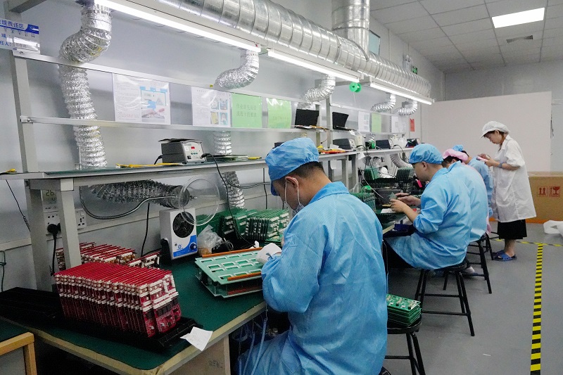
              You may also like