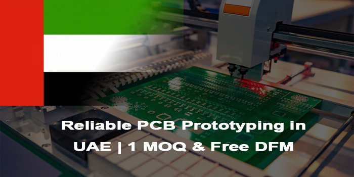
PCB Prototyping in UAE is a critical link in the electronics manufacturing chain, providing essential support for product development and iteration. EBest, a professional PCB manufacturer with 19 years of experience, delivers high-quality PCB prototyping in UAE services, covering custom solutions, fast delivery, and strict quality control to meet the diverse needs of local electronics projects.
Common Challenges of PCB Prototyping in UAE
- Can we get high-precision PCB prototypes that meet medical and aerospace industry standards?
- Is it possible to access PCB prototyping services with low MOQ and no unnecessary minimum order restrictions?
- How to solve the long lead time problem for urgent prototype needs?
- Can professional design checks be provided for free to avoid production failures in PCB prototyping?
- How to ensure the reliability of prototypes for high-stability application scenarios?
- Is there a PCB prototyping service that offers full production data traceability?
- Can custom requirements for special materials like ceramic and metal substrates be met in prototyping?
EBest’s Targeted Solutions to These Challenges
- For medical and aerospace high-precision requirements, we adopt advanced production equipment and strict process control, complying with ISO 13485 and AS9100D standards. Our material selection follows aerospace and medical-grade specifications, and our process parameters adhere to IPC Class 3 standards, ensuring each prototype meets industry-specific precision and reliability benchmarks.
- We offer 1-piece MOQ for all prototyping projects, eliminating the burden of unnecessary large orders. This supports small-batch testing, design iteration, and trial production needs, allowing you to validate concepts without financial constraints.
- To address long lead times, we provide a dedicated 24-hour expedited service. A specialized team prioritizes urgent orders, managing production scheduling, material preparation, and testing in parallel to ensure delivery within 24 hours without compromising quality.
- Every order includes free DFM analysis. Our team reviews Gerber files, BOMs, and layout drawings to identify potential issues like insufficient clearance, improper via placement, or component compatibility risks. We provide actionable feedback to correct flaws before production, reducing rework and revision cycles by up to 70%.
- We ensure prototype reliability through strict material control, full-process quality inspection, and MES system traceability. All materials undergo incoming inspection to eliminate defects, and production parameters are recorded in real time. Post-production testing includes electrical performance, temperature, and vibration checks to validate long-term stability.
- Our MES system enables full production data traceability. Every process step from material procurement to drilling, lamination, and inspection, is logged with unique identifiers, allowing you to review parameters and ensure accountability. This is critical for medical and aerospace projects requiring complete documentation.
- We specialize in custom solutions for special materials. Our process library includes ceramic substrates, metal-core PCBs, and high-frequency materials like Rogers. We leverage mature process technology to ensure consistent performance, even for high-power or high-temperature applications.
Why Choose EBest for PCB Prototyping in UAE?
Below are reasons why choose EBest for PCB prototyping in UAE:
- High First Article Success Rate: We achieve a 95%+ first article success rate, reducing rework time and project costs. Our strict process control and pre-production validation ensure prototypes meet functional requirements on the first attempt.
- 24-Hour Fast Prototyping: Our dedicated urgent team prioritizes production and testing, enabling delivery within 24 hours for time-sensitive projects. We maintain parallel workflows to avoid delays, even during peak demand.
- 99.2% On-Time Delivery Rate: We maintain a 99.2% on-time delivery rate, supported by intelligent production scheduling and reliable logistics. Real-time progress updates keep you informed throughout the process.
- 1 MOQ: We support orders as small as 1 piece, making us ideal for concept validation, design iteration, and small-scale testing.
- Customized Solutions: We tailor our services to your specific requirements, including material selection, layer count, and impedance control. Our team collaborates with you to optimize designs for performance and manufacturability.
- Free DFM Analysis: Our experienced engineers review your design files to identify and resolve potential issues before production, minimizing errors and accelerating time-to-market.
- 19 Years of Experience: Our technical team has delivered over 10,000 prototyping projects, handling complex designs for medical, aerospace, and industrial applications. We bring proven expertise to every project.
- Authoritative Certifications: We hold ISO 9001:2015, ISO 13485:2016, and AS9100D certifications, ensuring compliance with international quality standards. Our processes are audited annually to maintain consistency.
- MES System Traceability: Our MES system tracks all production data, providing complete transparency and accountability. This is critical for regulated industries requiring detailed documentation.
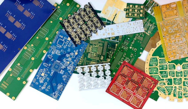
What Types of PCB Prototyping Services Can We Provide in the UAE?
Here are types of PCB prototyping services we can provide in UAE:
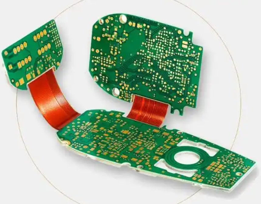
- Flexible PCBs: Suitable for compact, curved installations, widely used in industrial equipment and portable medical devices.
- Rigid PCBs: Including standard FR4 and high TG materials, offering stable performance for most electronic products and aerospace applications.
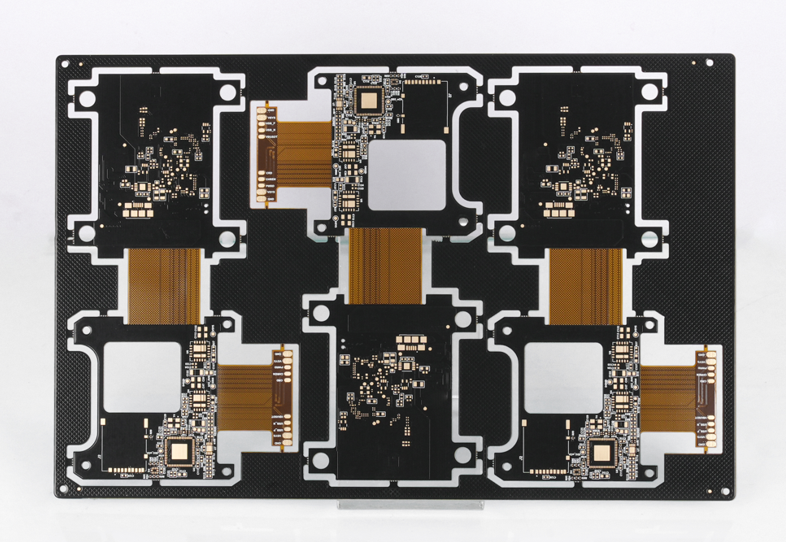
- Rigid-Flex PCBs: Combining rigid and flexible structures, ideal for complex assembly requirements in medical and aerospace fields.
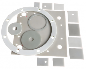
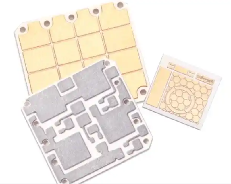
- Ceramic PCBs: Providing high temperature resistance and excellent insulation, suitable for high-power medical equipment and aerospace electronics.
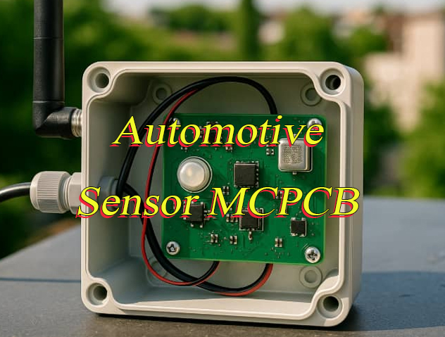
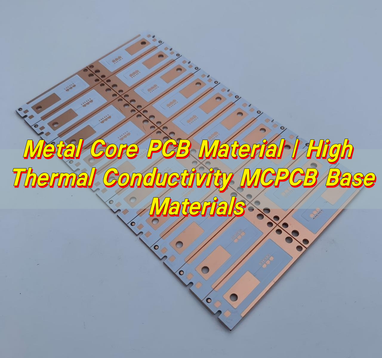
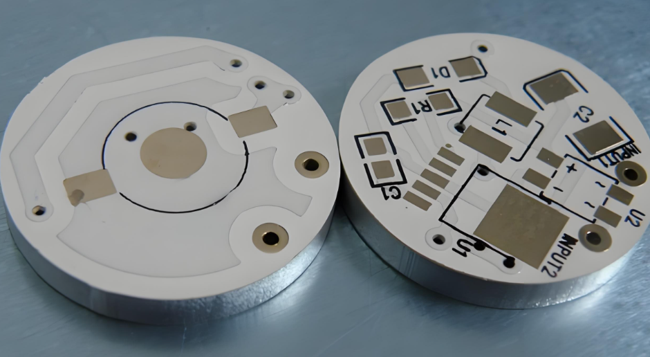
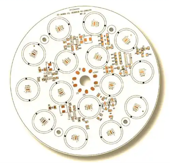
- Metal Core PCBs (MCPCBs): Delivering superior heat dissipation, ideal for industrial power supplies and medical imaging equipment.
- High-Frequency PCBs: Ensuring stable signal transmission for communication equipment and aerospace electronic systems.
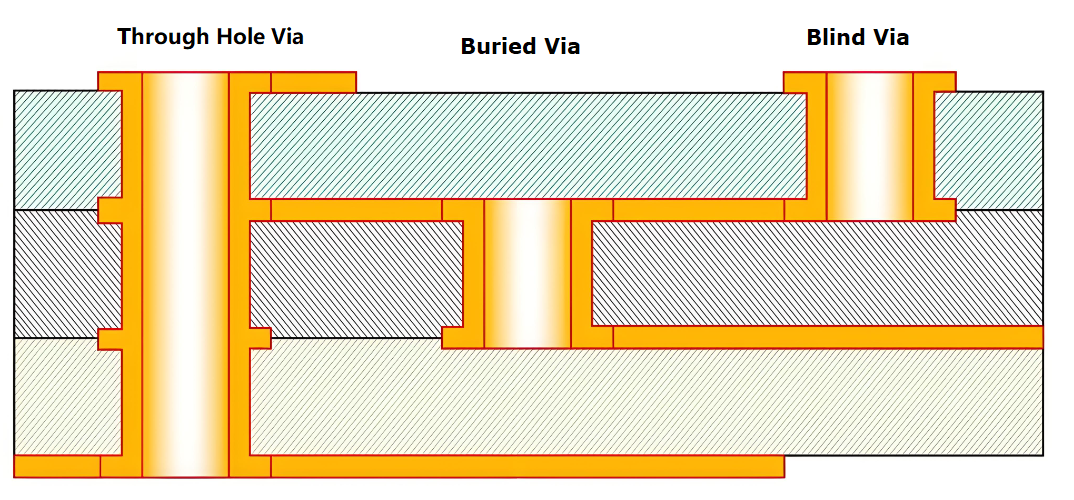
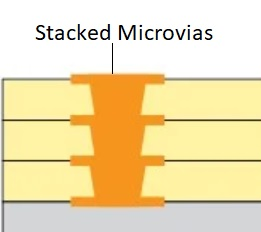
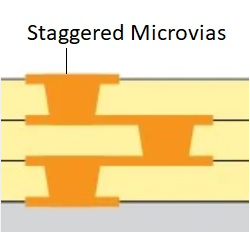
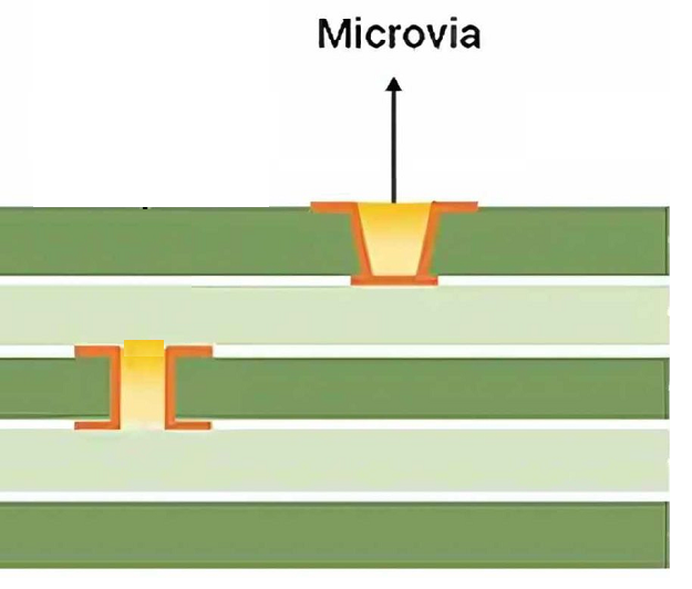
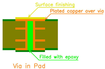
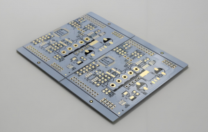
- Other Types: Including HDI, heavy copper, impedance-controlled, and single/double-sided boards, covering all common prototyping needs.
How Can We Ensure On-Time Delivery of PCB Prototyping Orders in the UAE?
Below are Methods about we ensure on-time delivery of PCB prototyping in UAE:
- Intelligent Production Scheduling: Our advanced scheduling system optimizes resource allocation, with real-time capacity monitoring to adjust for peak demand or material availability. This minimizes bottlenecks and ensures efficient workflow across all production stages.
- Dedicated Urgent Project Team: A specialized team manages expedited orders, with exclusive access to priority equipment and personnel. Parallel processing of fabrication and testing steps reduces overall cycle time without skipping quality checks.
- Strategic Logistics Partnerships: We collaborate with leading logistics providers to offer fast, secure transportation to the UAE. Real-time tracking allows you to monitor shipments from our facility to your location, with proactive updates on any potential delays.
- Pre-Production Validation: We conduct thorough pre-production checks, including design file verification, material confirmation, and BOM review. This eliminates last-minute delays caused by missing information, incorrect layer stacks, or component shortages.
- Transparent Progress Updates: We provide regular, detailed progress reports for every order, including fabrication status, test results, and shipping timelines. This transparency allows you to adjust project plans and communicate effectively with your team.
What Quality Checks Does EBest Do for UAE PCB Prototypes?
Here are quality checks for PCB prototyping in UAE:
- Incoming Material Inspection (IQC): All raw materials are tested for key parameters, including substrate dielectric constant, copper purity, and solder mask adhesion. Non-conforming materials are rejected before entering production.
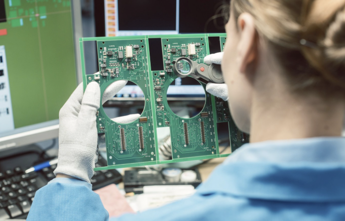
- In-Process Quality Control (IPQC): Real-time inspections during drilling, lamination, and etching detect defects early. We use statistical process control (SPC) to monitor parameters like layer alignment and plating thickness, correcting deviations before they affect quality.
- Automated Optical Inspection (AOI): High-resolution AOI systems scan all layers for surface defects, including trace irregularities, solder mask gaps, and component misalignment. Detection precision is ≤5μm, with a 99.5%+ rate for critical defects like opens and shorts.
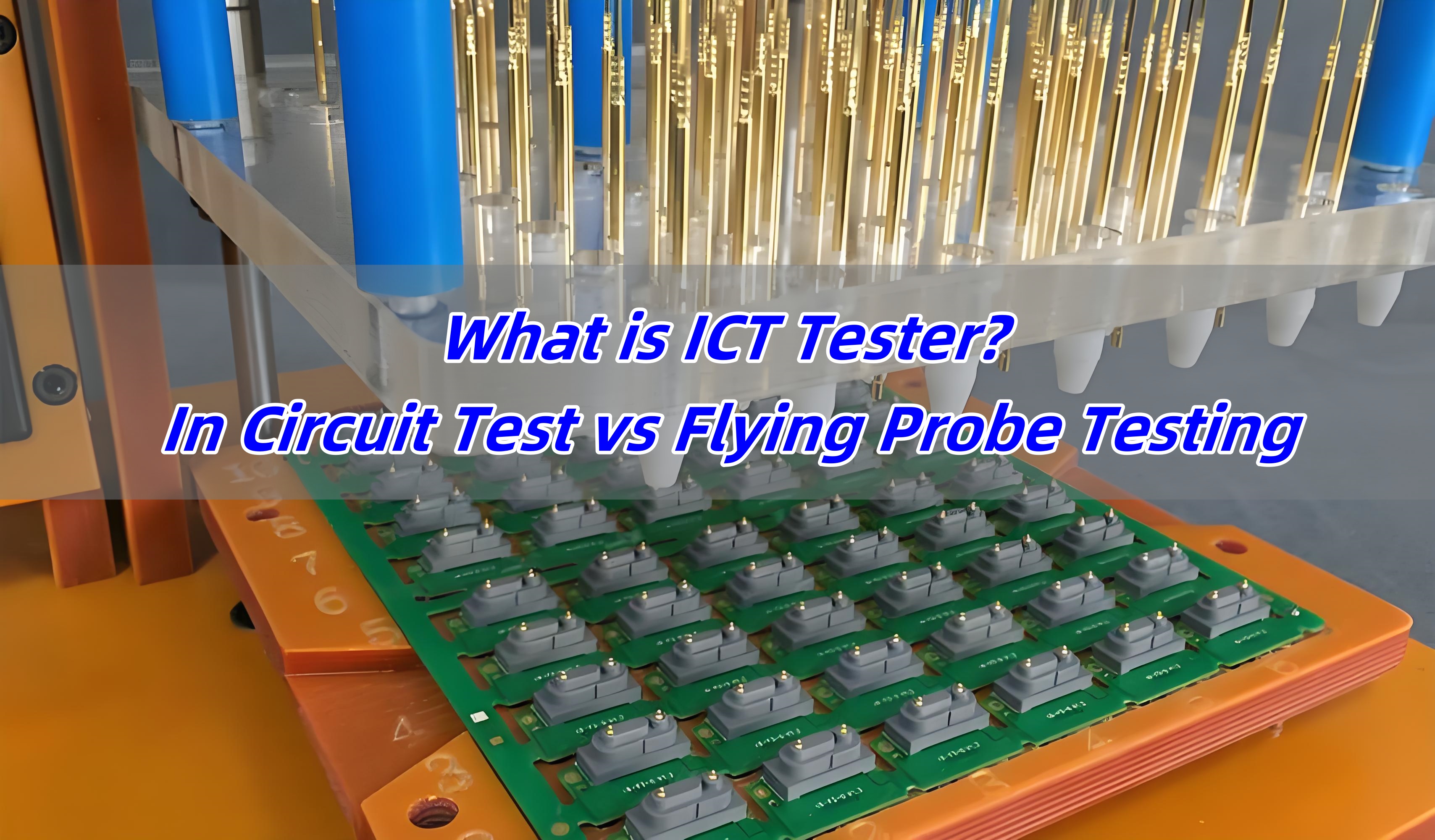
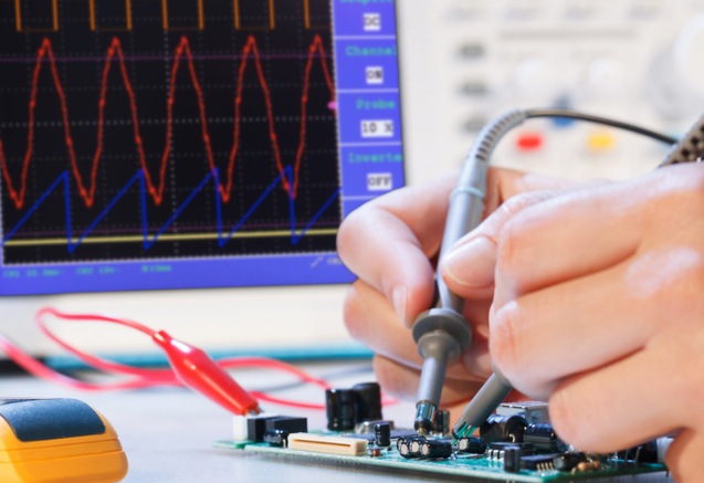
- Electrical Performance Testing: 100% of prototypes undergo flying probe testing, which verifies continuity, insulation resistance, and impedance without the need for custom test fixtures. This ensures all electrical connections meet design specifications.
- Environmental Stress Testing: For medical and aerospace applications, prototypes are subjected to thermal cycling (-40°C to 125°C), high humidity (85% RH at 85°C), and random vibration (5 Grms for 10 hours) to validate long-term reliability.
- Final Quality Inspection (FQC): A dedicated team performs a comprehensive final check, including visual inspection against IPC-A-600 Class 3 standards, functional testing, and documentation review. Only prototypes that pass all checks are shipped.
EBest’s UAE Prototyping Case Study: Medical Electrosurgical Generator
Project Background
A UAE-based medical device manufacturer was developing a compact electrosurgical generator for minimally invasive surgeries. The device required a prototype that could withstand high voltage, suppress electromagnetic interference (EMI), and comply with strict medical regulations.
Project Requirements
The prototype needed to meet ISO 13485 standards, withstand 3kV AC voltage, and limit EMI emissions to YY 0505 Class B levels. The design required a compact form factor (100mm × 80mm) with 4 layers, and the client requested a 5-day lead time with a first article success rate of 95% or higher.
Project Challenges
Key challenges included maintaining 3kV voltage resistance without increasing board size, reducing EMI from high-frequency circuits, and meeting the tight 5-day timeline while adhering to ISO 13485 quality controls. The prototype also needed to withstand autoclave sterilization (134°C, 3 bar pressure) for 1000 cycles.
Our Solutions
We assigned a cross-functional team with medical device experience to the project. We selected a high-TG FR4 substrate (Tg ≥ 170°C) and increased the creepage distance between high-voltage traces to 10mm, exceeding the 8mm minimum required for 3kV applications. To reduce EMI, we optimized the layout to separate analog and digital sections, added a solid copper ground plane, and included a copper foil shield around the high-frequency generator circuit, reducing emissions by 22dBμV/m.
We prioritized the order in our production schedule, with parallel processing of fabrication and testing. Our free DFM analysis identified a potential via placement issue near a high-voltage pad, which we corrected before production to avoid arcing risks. We also conducted pre-sterilization thermal testing to validate material durability.
Results:
We delivered the prototype in 4.5 days, 12 hours ahead of the client’s deadline. The first article success rate was 97%, exceeding the required 95%. Electrical testing confirmed the prototype withstood 3.5kV AC voltage (20% above specification) and met YY 0505 Class B EMI limits. Post-sterilization testing showed no degradation in performance after 1000 autoclave cycles, with all electrical parameters remaining within tolerance. The client integrated the prototype into their device, accelerating their product launch by 2 weeks, and has since placed regular orders for both prototyping and low-volume production.
FAQs of PCB Prototyping in UAE
Q1: Can EBest handle urgent prototype orders in the UAE?
A1: Yes, we offer a dedicated 24-hour expedited service for urgent orders. Our specialized team uses priority production slots and pre-stocked materials to fabricate, test, and ship prototypes within 24 hours. We maintain full quality control throughout, including AOI and electrical testing, to ensure performance meets your requirements.
Q2: What is the minimum order quantity for prototyping at EBest?
A2: Our minimum order quantity is 1 piece for all prototyping projects. This allows you to validate single design iterations or small-batch tests without the cost of excess units, supporting flexible and efficient product development.
Q3: Does EBest provide free DFM analysis for prototype orders?
A3: Yes, every order includes a free, comprehensive DFM analysis. Our engineers review your design files to identify manufacturability issues and provide annotated reports with actionable fixes. This reduces rework and ensures your prototype is production-ready from the first attempt.
Q4: How does EBest ensure quality for medical prototyping projects?
A4: We comply with ISO 13485 standards for all medical projects, using certified medical-grade materials and enforcing strict process controls. Our MES system provides full traceability, and we conduct specialized testing, including sterilization resistance and biocompatibility screening, to meet medical device requirements.
Q5: Can EBest support aerospace prototyping projects in the UAE?
A5: Yes, we hold AS9100D certification and follow IPC Class 3 standards for aerospace projects. We use aerospace-grade materials, such as high-strength FR4 and Rogers laminates, and conduct extreme environmental testing to ensure prototypes perform in space and aviation environments.
Choose EBest for Your UAE PCB Prototyping Needs
EBest delivers reliable, high-quality prototyping services tailored to the UAE’s unique engineering requirements. Our 19 years of experience, combined with 24-hour expedited service, 1-piece MOQ, and free DFM analysis, ensures your projects stay on schedule and meet the highest quality standards. Whether for medical devices, aerospace systems, or industrial equipment, we have the expertise to bring your designs to life. Contact us today to place your order via email: sales@bestpcbs.com.