If you work with electronic devices, you’ve probably heard of PCB thermal conductivity. But do you know what it really means? Or why it matters for your projects? This guide breaks down everything you need to know—from key materials to design tips
What Is PCB Thermal Conductivity?
PCB thermal conductivity refers to the ability of a printed circuit board material to transfer heat from one location to another. It is typically measured in W/m·K (Watts per meter-Kelvin).
A higher thermal conductivity value means heat travels more efficiently through the board. This helps prevent local hot spots and keeps electronic components operating within safe temperature limits.
Electronic components generate heat during operation. If the PCB cannot dissipate this heat effectively, several problems may occur:
- Component overheating
- Reduced electrical performance
- Accelerated material aging
- Solder joint fatigue
- Unexpected system failure
Because of these risks, thermal performance is now a critical parameter in PCB design.

What Is PCB Thermal Conductivity?
Why Thermal Conductivity is Important in PCB?
Thermal conductivity becomes especially important in systems such as:
- LED lighting modules
- automotive power electronics
- RF communication equipment
- industrial motor controllers
- high-density computing hardware
In these systems, components like MOSFETs, power regulators, and RF amplifiers can generate significant heat during operation. A properly designed PCB spreads that heat efficiently across copper planes and into external cooling systems.
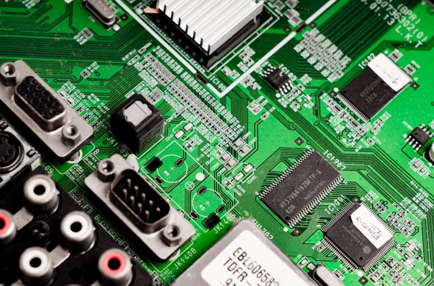
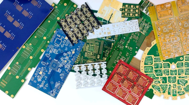
Thermal Conductivity of Common PCB Materials
Different PCB materials conduct heat at different rates. The base laminate, metal layers, and structural design all influence overall thermal performance.
The following table shows typical thermal conductivity values for common PCB materials.
| PCB Material | Thermal Conductivity (W/m·K) | Typical Applications |
| FR-4 Standard Laminate | 0.3 – 0.4 | Consumer electronics |
| High-Tg FR-4 | 0.4 – 0.6 | Industrial electronics |
| Aluminum PCB | 1 – 3 | LED lighting, power modules |
| Copper | ~385 | Heat spreading layer |
| Ceramic (Alumina) | 20 – 30 | RF modules, high-power circuits |
| Aluminum Nitride (AlN) | 140 – 180 | High-power semiconductor modules |
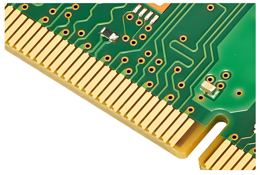
Most standard PCBs use FR-4 epoxy glass laminate. While FR-4 is cost-effective and electrically stable, its thermal conductivity is relatively low. This is why designers often rely on copper planes and thermal vias to improve heat flow.
Which PCB Material Has the Highest Thermal Conductivity?
Among commonly used PCB materials, ceramic substrates offer the highest thermal conductivity.
Aluminum nitride (AlN) stands out because it combines high thermal conductivity with excellent electrical insulation. Its thermal conductivity can exceed 170 W/m·K, which is hundreds of times higher than standard FR-4. Despite its excellent thermal properties, AlN is significantly more expensive than FR-4. Manufacturing complexity is also higher.
Therefore, ceramic PCBs are usually reserved for applications that require extreme thermal performance, such as:
- power semiconductor modules
- high-frequency RF systems
- aerospace electronics
- high-power laser drivers
For most industrial products, aluminum PCB or optimized FR-4 stack-ups provide sufficient thermal performance at a more reasonable cost.
How Does Copper Thickness Affect PCB Thermal Conductivity?
Copper plays a major role in PCB heat spreading. Although the base laminate may have low thermal conductivity, copper traces and planes help move heat away from components. Copper has a thermal conductivity of approximately 385 W/m·K, which is extremely high compared with FR-4.
Increasing copper thickness improves thermal performance in several ways:
- Thicker copper spreads heat across a larger area.
- Reduced resistance helps decrease power loss.
- Heat moves more evenly through copper planes.
Typical PCB copper thickness values include:
| Copper Weight | Thickness |
| 1 oz | ~35 µm |
| 2 oz | ~70 µm |
| 3 oz | ~105 µm |
| 4 oz | ~140 µm |
Power electronics designs often use 2 oz or thicker copper. Heavy copper PCBs can reach 6 oz or even higher for extreme current applications. However, thicker copper also introduces design considerations:
- trace spacing requirements increase
- etching becomes more challenging
- manufacturing cost rises
Therefore, engineers usually balance copper thickness with other thermal management methods such as thermal vias and heat sinks.
How Can You Improve PCB Thermal Conductivity in Design?
Even when using standard FR-4 materials, designers can significantly improve heat dissipation through thoughtful PCB layout and structure. Several design techniques are commonly used.
1. Use Larger Copper Planes
Copper planes distribute heat across the board surface, you can use large ground planes or power planes act as heat spreaders.
2. Add Thermal Vias
Thermal vias create vertical heat paths between layers. They allow heat to move from the component side to inner copper planes or heat sinks.
3. Select Metal Core PCB
Metal core PCBs use aluminum or copper substrates. These materials improve thermal conductivity and enable efficient heat transfer.
4. Optimize Component Placement
Components that generate significant heat should not be crowded together. Proper spacing helps air circulation and reduces temperature buildup.
5. Use Heat Sinks
External heat sinks remove heat from the PCB and release it into the surrounding environment.
What Is the Difference Between Thermal Conductivity and Thermal Resistance in PCB?
Thermal conductivity and thermal resistance are related but different concepts.
- Thermal conductivity describes how well a material conducts heat.
- Thermal resistance measures how difficult it is for heat to travel through a structure.
The relationship can be expressed as:
Thermal Resistance = Thickness / (Thermal Conductivity × Area)
In PCB design, this means:
- thicker materials increase thermal resistance
- higher conductivity materials reduce resistance
- larger heat transfer areas improve cooling
Designers often calculate thermal resistance when evaluating cooling performance. A lower thermal resistance means heat can flow away from components more easily.
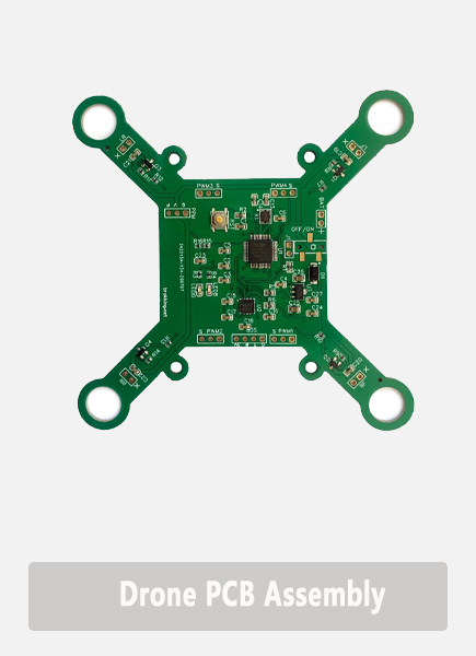
Where Are High Thermal Conductivity PCBs Used?
High thermal conductivity PCBs appear in many modern electronic systems. As power density increases, thermal design becomes more critical.
Common applications include:
- LED lighting systems
- automotive control modules
- power converters and inverters
- telecom base stations
- RF amplifiers
- industrial automation equipment
Similarly, power electronics used in electric vehicles require efficient thermal management. Heavy copper PCBs and thermal vias help maintain stable operating temperatures. In RF systems, excessive heat can affect signal stability, thermal control therefore supports both reliability and electrical performance.
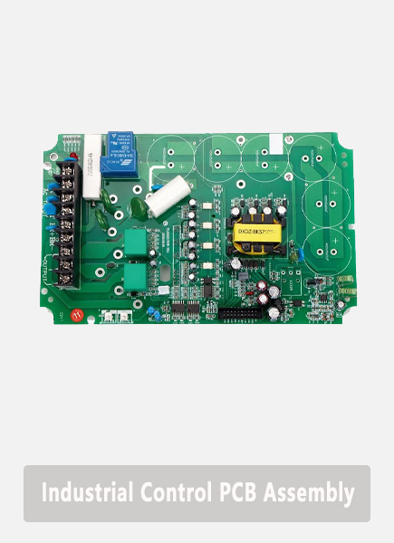
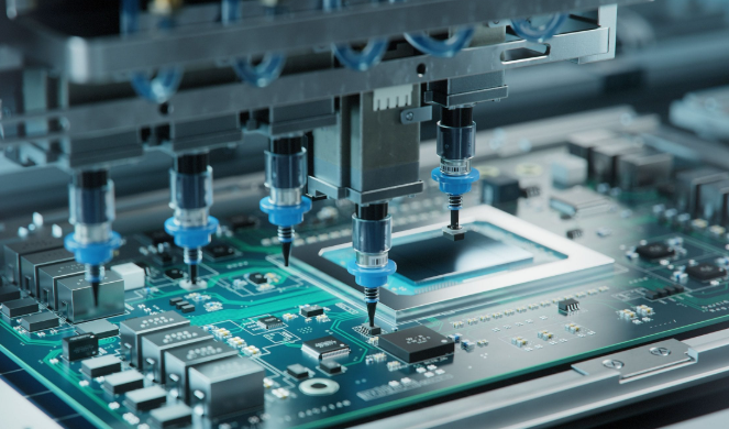
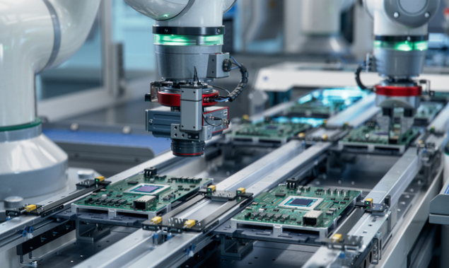
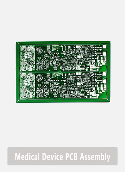
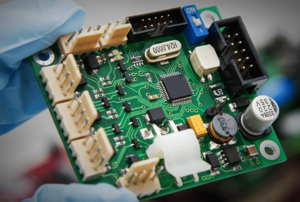
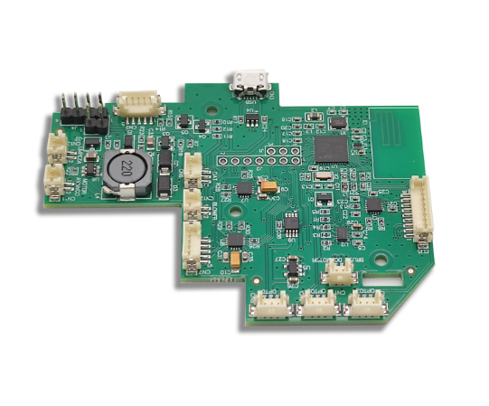
Why Choose EBest as Your High Thermal Conductivity PCB Manufacturer?
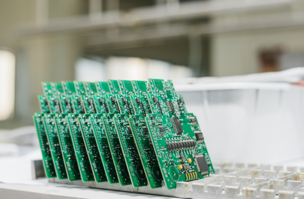
At EBest Circuit (Best Technology), we focus on supporting engineers who require reliable PCB fabrication and assembly solutions for high-performance electronics. Our team has over 19 of experience in PCB and PCBA manufacturing. Our facilities operate in both China and Vietnam, allowing us to support global supply chains and flexible production requirements.
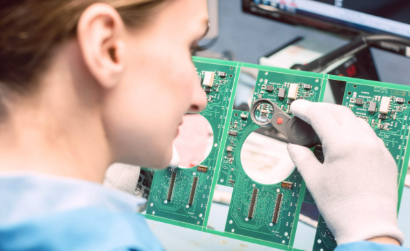
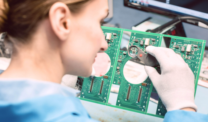
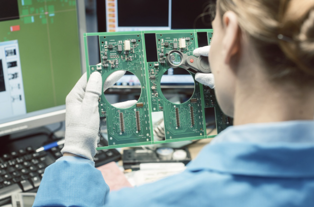
We work closely with customers during the early engineering stage. Our engineering team reviews design files and provides practical DFM feedback that helps improve manufacturability and thermal performance.
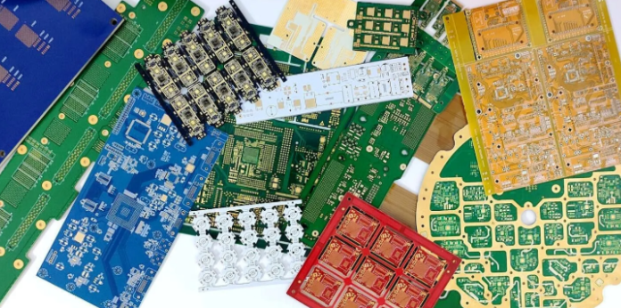
Our capabilities include:
- multilayer PCB fabrication up to complex stack-ups
- aluminum PCB and metal core PCB manufacturing
- heavy copper PCB production
- thermal via drilling and filling technologies
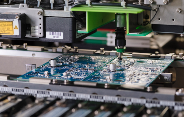
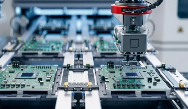
- SMT and THT assembly services
- component sourcing and turnkey PCBA
For PCB fabrication, thermal design consultation, or turnkey PCBA services, feel free to contact our team at sales@bestpcbs.com.
FAQ About PCB Thermal Conductivity
1. How can I improve PCB heat dissipation?
Several design methods improve PCB heat dissipation. Common techniques include:
- using thicker copper layers
- adding thermal vias
- increasing copper plane area
- selecting aluminum PCB substrates
- attaching external heat sinks
2. What PCB material is best for thermal management?
Ceramic materials such as aluminum nitride offer the highest thermal conductivity. However, aluminum PCBs provide an excellent balance between cost and performance. Many LED and power electronics systems use aluminum substrates. For general applications, optimized FR-4 with thermal vias can also deliver effective thermal management.
3. Does thicker copper improve thermal conductivity?
Yes. Thicker copper improves heat spreading across the board. Copper conducts heat extremely well. Increasing copper thickness creates larger thermal paths that help distribute heat more evenly.
4. Is aluminum PCB better for heat dissipation?
Yes. Aluminum PCBs provide significantly better heat dissipation than standard FR-4 boards.
The aluminum base acts as a heat spreader and transfers heat quickly to external cooling systems.