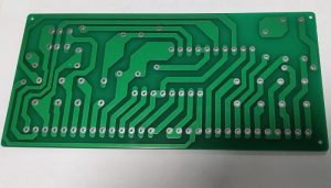
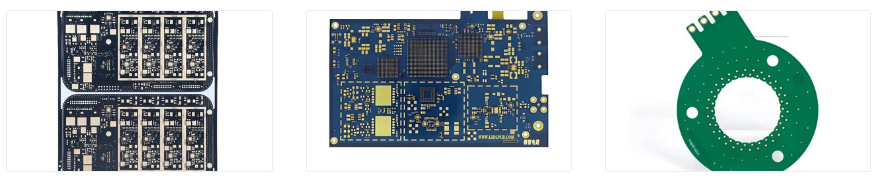
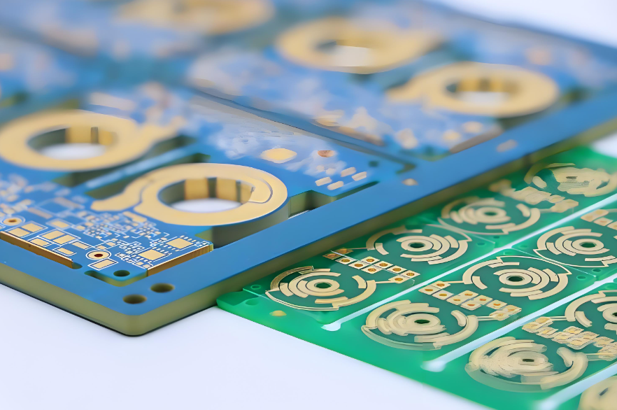
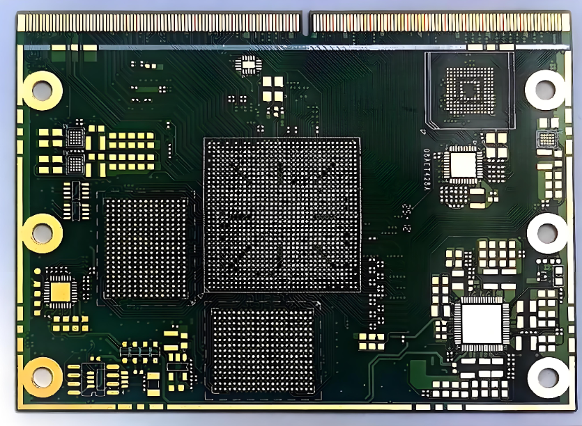
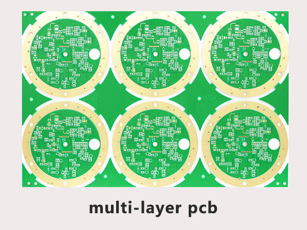
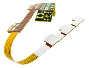
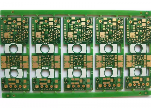
A multi-layer PCB is a printed circuit board with more than two copper layers, designed to support complex circuits, high-speed signals, and compact electronic systems. Compared with single-sided or double-sided boards, a multi-layer printed circuit board offers higher routing density, improved EMI control, and better electrical performance.
As modern electronics become smaller and more powerful, engineers increasingly rely on high-density multi-layer PCB design to meet performance and space requirements. In this guide, you will learn how multi-layer PCBs work, their structure, manufacturing process, and how to choose the right multi-layer PCB manufacturer.
What Is a Multi-Layer PCB?
A multi-layer PCB is constructed by laminating multiple copper layers together using insulating materials such as FR4 cores and prepreg (PP). These layers are electrically connected through plated vias, including through holes, blind vias, and buried vias.
Common configurations include:
- 4 layer PCB – Entry-level for signal and power separation
- 6 layer PCB – Improved EMI control and routing flexibility
- 8 layer PCB – Suitable for high-speed digital circuits
- 10 layer PCB and 12 layer PCB – Used in industrial and embedded systems
- 20 layer PCB and 32 layer PCB – Advanced applications such as aerospace, servers, and high-performance electronics
This layered structure allows engineers to allocate different functions to different layers, such as signal routing, power distribution, grounding, and shielding.
Why Use Multi-Layer Printed Circuit Boards?
A multi-layer printed circuit board is essential when circuit complexity increases or when performance requirements exceed what a double-sided PCB can handle.
Key advantages include:
- Higher circuit density in limited board space
- Better signal integrity for high-speed applications
- Improved EMI shielding through dedicated ground planes
- Stable power distribution with internal power layers
- Support for HDI structures such as blind and buried vias
- Reduced product size and weight
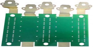
Multi-layer PCBs are widely used in communication equipment, automotive electronics, medical devices, industrial control systems, aerospace electronics, and consumer electronics.
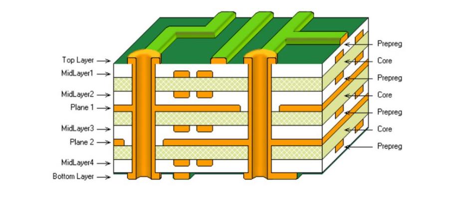
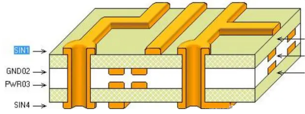
What Is the Structure of a Multi-Layer PCB?
A typical multi-layer PCB stack-up consists of alternating conductive and insulating layers. Each layer serves a specific function to ensure electrical performance and mechanical stability.
| Layer | Function |
|---|---|
| Top Silkscreen / Legend | Marks component labels, polarity, part numbers, date codes, and assembly information. |
| Top Surface Finish | Protects exposed copper from oxidation and improves solderability. |
| Top Solder Mask | Protects copper traces and prevents unwanted solder bridging during SMT assembly. |
| Top Copper Layer | Carries signals, power, or ground according to the PCB design. |
| Core Material | Provides mechanical support and electrical insulation, commonly using FR4 or FR5. |
| Prepreg / PP | Bonds copper layers and core materials during lamination. |
| Inner Copper Layers | Used for signal routing, power planes, ground planes, EMI shielding, or controlled impedance design. |
| Bottom Copper Layer | Provides additional routing and connection functions. |
| Bottom Solder Mask | Protects bottom-side copper and improves assembly reliability. |
| Bottom Surface Finish | Protects exposed copper pads and supports soldering. |
| Bottom Silkscreen / Legend | Marks bottom-side components, polarity, test points, and production information. |
A well-designed multi-layer PCB stack-up directly impacts impedance control, thermal performance, and signal quality.
How Do Blind and Buried Vias Improve Multi-Layer PCB Design?
In high-density designs, engineers often use blind and buried vias PCB technology to optimize routing and reduce board size.
- Blind vias connect outer layers to one or more inner layers without passing through the entire board.
- Buried vias connect internal layers only and are not visible from the outside of the PCB.
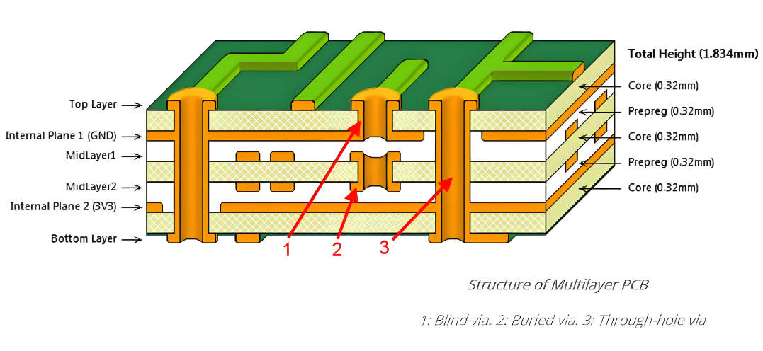
These via structures help increase routing space, improve signal performance, and support BGA, fine-pitch components, and compact HDI layouts. They are especially useful in high-density multi-layer PCB and advanced electronic designs.
What Materials Are Used in Multi-Layer PCB Fabrication?
Material selection plays a critical role in multi-layer PCB fabrication, especially for thermal stability, dimensional control, and long-term reliability.
| Material Type | Typical Use |
|---|---|
| FR4 | Standard material for most FR4 multi-layer PCB applications. |
| High Tg FR4 | Recommended for high Tg multi-layer PCB designs, especially boards above 8 layers. |
| FR5 | Used where better thermal and electrical performance is required. |
| Rogers / PTFE | Used for high-frequency and RF applications. |
For boards above 8 layers, high Tg material is often preferred because it provides better heat resistance, improved dimensional stability, and stronger reliability during PCB assembly.
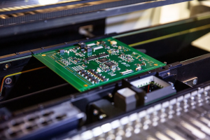
What Is the Multi-Layer PCB Manufacturing Process?
The multi-layer PCB manufacturing process involves several precise steps to ensure layer alignment, electrical conductivity, mechanical strength, and long-term reliability.
1. Inner layer imaging and etching
2. Oxide treatment for better bonding
3. Lamination with prepreg and core materials
4. Drilling for through holes, blind vias, or buried vias
5. Copper plating
6. Outer layer patterning
7. Solder mask application
8. Surface finishing, such as ENIG, HASL, OSP, immersion silver, or immersion tin
9. Silkscreen printing
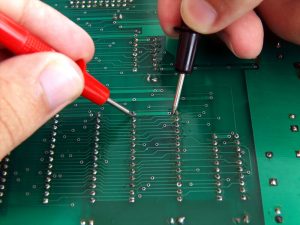
10. Electrical testing, AOI inspection, and other quality checks when required
Each step requires tight process control, especially for custom multi-layer PCB fabrication with high layer counts, fine traces, impedance control, or advanced via structures. For whole multi-layer PCB manufacturing process, please view our video:
How Much Does a Multi-Layer PCB Cost?
The multi-layer PCB cost depends on multiple engineering and manufacturing factors. A 4 layer PCB is usually more cost-effective than a 12 layer PCB or 32 layer PCB, while advanced via structures and tighter tolerances will also affect pricing.
Major cost factors include:
- Layer count
- Material type
- Board thickness
- Copper thickness
- Blind via or buried via design
- Surface finish
- Controlled impedance requirements
- Production quantity
- Testing and inspection standards
Early DFM review can help optimize the stack-up, reduce production risk, and control the total cost of multi-layer PCB fabrication.
What Is the Lead Time for Multi-Layer PCB?
The multi-layer PCB lead time varies based on layer count, material availability, production volume, and manufacturing complexity.
| PCB Type | Typical Lead Time |
|---|---|
| 4 layer PCB prototype | About 3–5 working days |
| 6 layer PCB or 8 layer PCB | About 5–8 working days |
| 10 layer PCB or 12 layer PCB | About 7–12 working days |
| 16 layer PCB and above | Depends on design complexity and material requirements |
For quick turn multi-layer PCB projects, expeited production may be available after engineering review. For an exact lead time, it is best to send Gerber files, stack-up requirements, and technical specifications to the manufacturer.
How to Choose a Reliable Multi-Layer PCB Manufacturer?
Choosing the right multi-layer PCB supplier directly affects product quality, assembly reliability, and delivery performance. A professional supplier should offer more than basic board production. Engineering support is equally important.
When selecting a multi-layer PCB manufacturer, consider the following points:
- Experience in multi-layer PCB manufacturing
- Capability for 4L to 32L boards
- Support for blind vias, buried vias, and HDI structures
- DFM review and stack-up support
- Stable material sourcing
- Strict quality inspection and electrical testing
- Capability for both PCB fabrication and multi-layer PCB assembly
A reliable manufacturer can help engineers improve manufacturability, reduce design risk, and move faster from prototype to production.
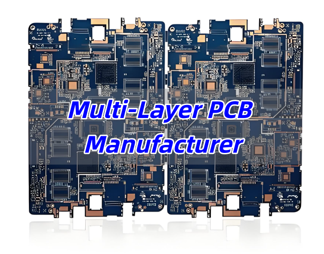
Why Choose EBest Circuit for Multi-Layer PCB Fabrication?
EBest Circuit is a professional multi-layer PCB manufacturer offering custom multi-layer PCB fabrication from 4 layer PCB to 32 layer PCB. We support prototypes, small-batch production, and mass production for customers in industrial, medical, automotive, communication, aerospace, and consumer electronics markets.
Our engineering team provides support for multi-layer PCB design, stack-up review, DFM analysis, impedance control, material selection, and assembly requirements. Whether you need an FR4 multi-layer PCB, a high Tg multi-layer PCB, or a high-density board with blind and buried vias, we can help evaluate manufacturability before production.
Our advantages include:
- 4L–32L multi-layer PCB fabrication capability
- Support for custom multi-layer PCB stack-up design
- Experience with high Tg FR4 and HDI structures
- Blind via and buried via manufacturing capability
- Fast turnaround for multi-layer PCB prototype projects
- One-stop multi-layer PCB assembly service
- Strict quality control and electrical testing
- Engineering support from prototype to mass production
If you are developing a complex electronic product and need a reliable multi-layer PCB supplier, EBest Circuit can provide professional support from design review to finished board delivery.
FAQs About Multi-Layer PCB
1. What is the difference between a multi-layer PCB and a double-sided PCB?
A double-sided PCB has two copper layers, while a multi-layer PCB has more than two copper layers. Multi-layer boards provide more routing space, better EMI control, and stronger electrical performance for complex circuits.
2. How many layers can a PCB have?
PCB layer count depends on design requirements and manufacturing capability. Common designs include 4 layer PCB, 6 layer PCB, 8 layer PCB, 10 layer PCB, and 12 layer PCB. Advanced applications may require 20 layer PCB or 32 layer PCB.
3. When should I use a high Tg multi-layer PCB?
A high Tg multi-layer PCB is recommended when the board has a high layer count, high assembly temperature, or strict reliability requirements. It is especially useful for boards above 8 layers and products used in demanding environments.
4. Are blind vias and buried vias necessary for all multi-layer PCBs?
No. Standard through holes are enough for many designs. Blind vias and buried vias are mainly used when the PCB requires high routing density, smaller size, BGA fan-out, or HDI performance.
5. What files are needed for multi-layer PCB fabrication?
For quotation and production, manufacturers usually need Gerber files, drill files, stack-up information, material requirements, copper thickness, surface finish, solder mask color, silkscreen color, and any special impedance or testing requirements.
6. Can EBest Circuit provide multi-layer PCB assembly?
Yes. EBest Circuit provides both multi-layer PCB fabrication and multi-layer PCB assembly. This one-stop service helps reduce communication time, improve production consistency, and support faster project delivery.
Final Thoughts
A multi-layer PCB is an essential solution for modern electronic products that require high density, compact size, stable power distribution, and reliable signal performance. From 4 layer PCB prototypes to 32 layer high-density boards, every detail matters, including material selection, stack-up design, via structure, fabrication control, and assembly process.
If you are looking for a reliable multi-layer PCB manufacturer for custom multi-layer PCB fabrication or multi-layer PCB assembly, EBest Circuit is ready to support your project from engineering review to production.
Contact us today for multi-layer PCB quotation and technical support:
Email: sales@bestpcbs.com
Email: sales@bestpcb.vn