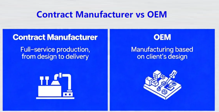
What is a Contract Manufacturer (CM)?
A contract manufacturer (CM) is a company hired to build products based on a customer’s design and specifications. The customer provides engineering files, bills of materials, and assembly instructions. The contract manufacturer focuses on production execution.
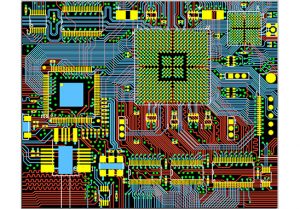
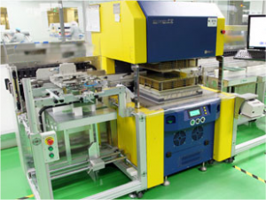
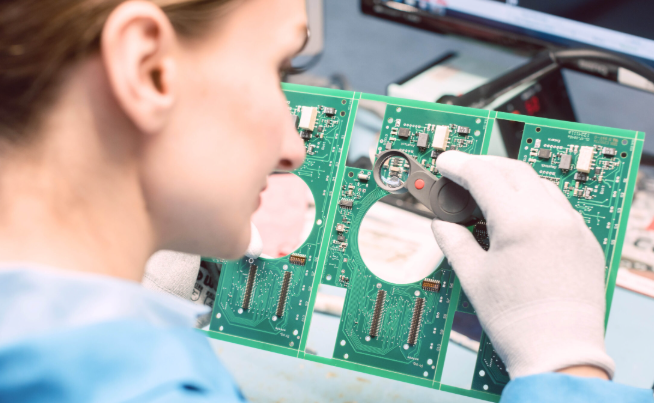
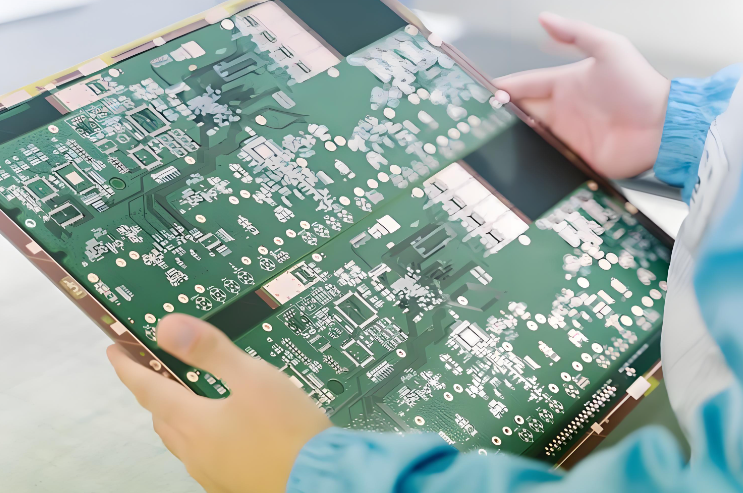
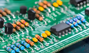
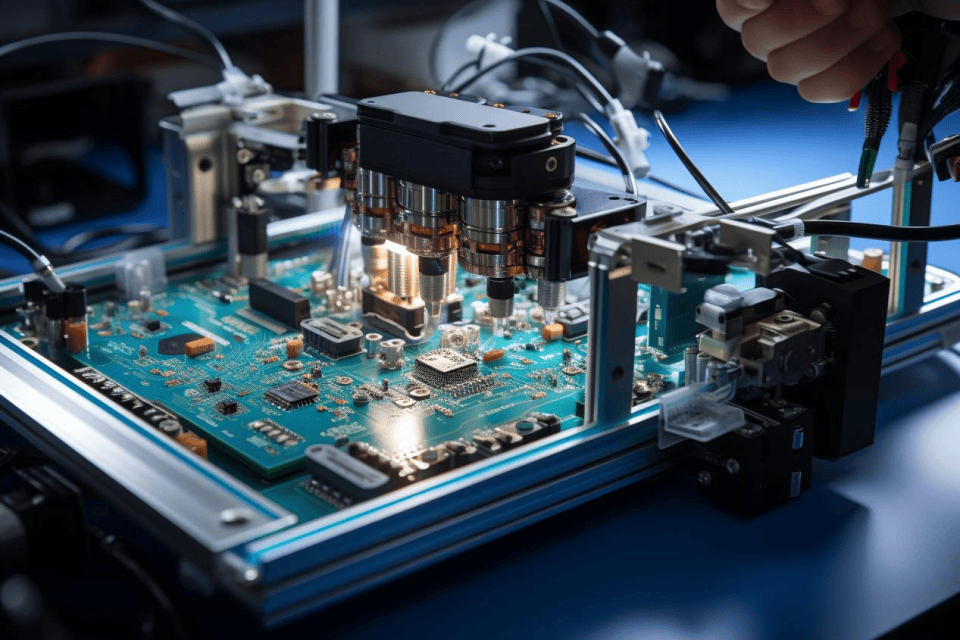
In electronics manufacturing, this model is common in PCB assembly, device production, and box-build services. The client retains ownership of the product design while the CM handles the manufacturing process. Contract manufacturers operate as production specialists. Their factories often include SMT lines, testing equipment, and supply chain systems designed for high efficiency.
Typical services provided by contract manufacturers include:
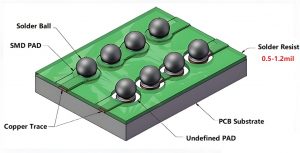
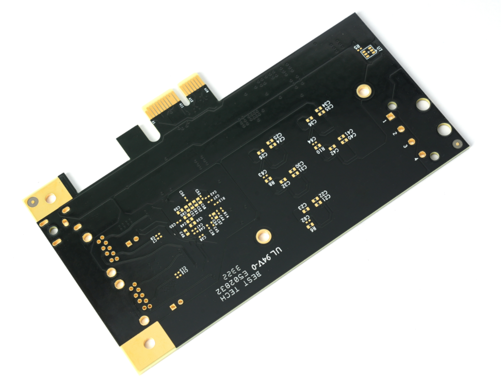
- PCB fabrication and PCB assembly
- Component sourcing and supply chain management
- SMT and through-hole assembly
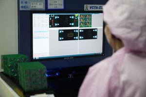
- Functional testing and inspection
- Product assembly and box-build services
- Packaging and logistics support
For many companies, working with a CM allows them to scale production without building expensive factories. Engineering teams focus on innovation while manufacturing experts handle production complexity.
What is an Original Equipment Manufacturer (OEM)?
An original equipment manufacturer (OEM) traditionally refers to a company that designs and produces products under its own brand or intellectual property. The OEM is the originator of the product concept. In many industries, OEMs design systems, define product specifications, and control the product lifecycle. The manufacturing stage may happen internally or through external partners.
For example, a company developing a medical imaging device may act as the OEM. It creates the product architecture, develops the software, and owns the technology. Production may still be outsourced to a contract manufacturer.
In electronics and hardware industries, OEMs typically handle:
- Product design and engineering
- Intellectual property ownership
- Brand development and marketing
- Product certification and compliance
- Market distribution and customer support
The OEM owns the product identity. Even when manufacturing is outsourced, the OEM remains responsible for the product’s performance and reputation. OEM companies often invest heavily in research and development. Their teams include electrical engineers, mechanical designers, firmware developers, and product managers.
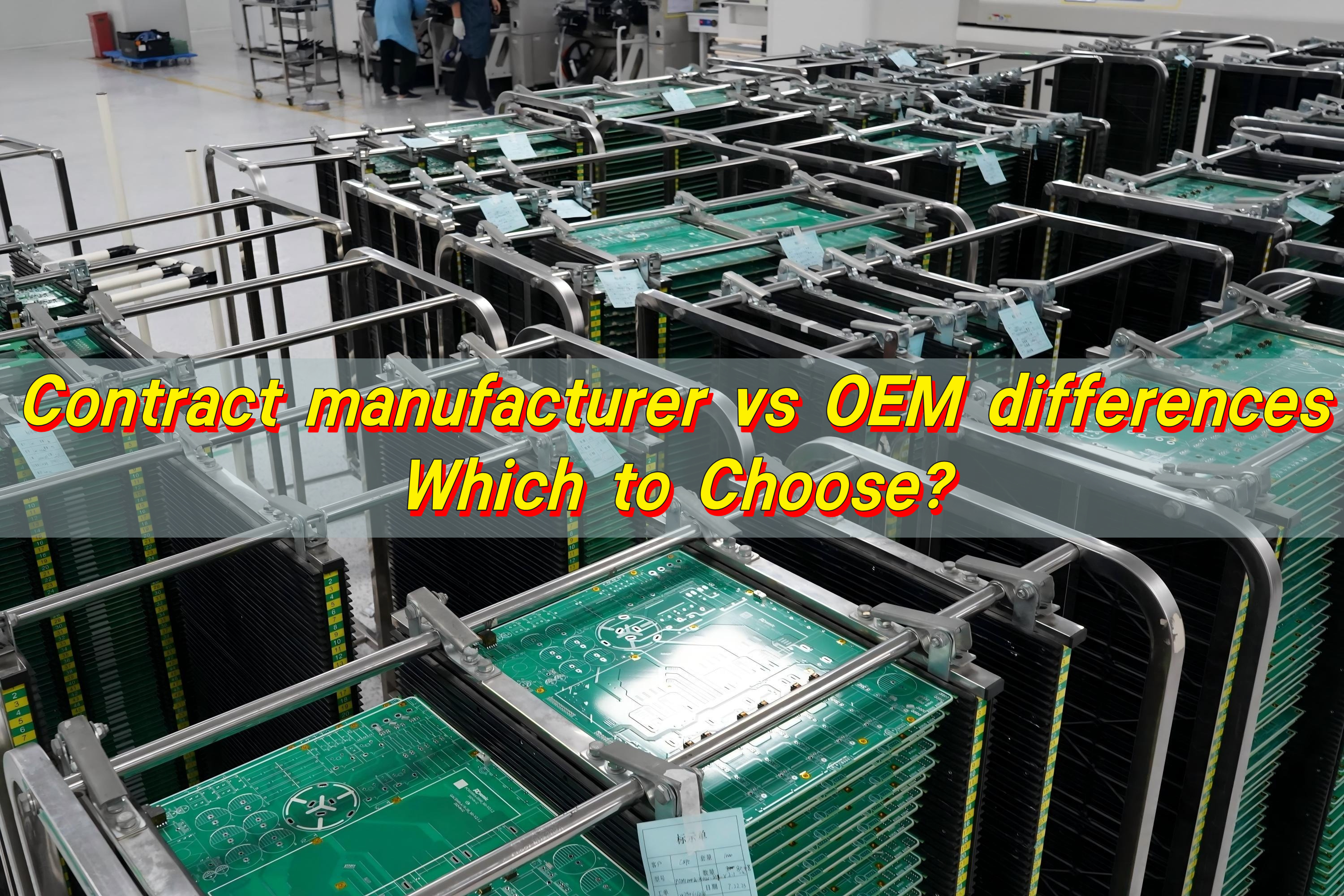
What is the Difference Between OEM and Contract Manufacturer?
The core difference between these two models lies in responsibility and ownership. The OEM creates and owns the product concept. The contract manufacturer builds the product. Both roles are essential in modern supply chains. Many successful products depend on collaboration between the two.
The OEM develops the product. The CM produces it efficiently at scale:
- OEM – Product creator and brand owner
- Contract Manufacturer – Production partner executing manufacturing tasks
| Aspect | OEM | Contract Manufacturer |
|---|---|---|
| Product Design | Created by OEM | Provided by customer |
| Intellectual Property | Owned by OEM | No ownership |
| Brand Ownership | OEM brand | No brand involvement |
| Manufacturing Responsibility | May outsource | Performs production |
| Engineering Control | Full design authority | Manufacturing engineering only |
| Market Strategy | Managed by OEM | Not involved |
| Revenue Source | Product sales | Manufacturing service fees |
OEM companies prioritize innovation, market positioning, and product differentiation. Contract manufacturers prioritize process efficiency, production quality, and cost optimization. Both roles complement each other. Many large technology companies operate successfully using this partnership model.
Contract Manufacturer vs OEM: Who Owns the Design?
Design ownership is one of the most important factors when comparing contract manufacturer vs OEM differences.
In almost every case, the OEM owns the product design. The OEM invests in research and development. It creates the product architecture and defines the functionality. This intellectual property belongs to the OEM. The contract manufacturer receives the design files and uses them to build the product.
Typical documentation provided to a CM includes:
- PCB Gerber files
- Assembly drawings
- Bill of materials (BOM)
- Test procedures
- Firmware or software packages
The contract manufacturer does not claim ownership of these assets. It operates under manufacturing agreements that protect the customer’s intellectual property. However, contract manufacturers often contribute engineering suggestions. These recommendations help improve manufacturability and reduce cost.
Common support provided by experienced CMs includes:
- DFM (Design for Manufacturability) feedback
- Component substitution advice
- Process optimization suggestions
- Assembly yield improvements
Despite these contributions, the final product design still belongs to the OEM. This arrangement protects innovation while allowing production experts to refine the manufacturing process.
What Are the Pros and Cons of Contract Manufacturing?
Contract manufacturing has become a preferred production model across many industries. It allows companies to launch products without building large factories. However, like any strategy, it offers advantages and limitations.
Many companies adopt contract manufacturing because it offers strong operational benefits. Key advantages include:
- Lower capital investment
- Access to experienced manufacturing teams
- Scalable production capacity
- Faster product launches
- Reduced operational complexity
Instead of investing millions in equipment, companies can leverage an existing manufacturing ecosystem. Contract manufacturers already operate advanced production lines, quality systems, and supply chain networks. This infrastructure allows faster product ramp-up.
Another advantage is geographic flexibility. Production can be located near component suppliers or logistics hubs. This reduces shipping time and improves supply chain resilience.
Although contract manufacturing offers many benefits, companies should evaluate potential challenges carefully. These may include:
- Less direct control over production operations
- Dependence on external manufacturing partners
- Communication gaps during complex projects
However, these challenges can often be minimized through strong partnerships and clear project management. Many companies maintain engineering teams that work closely with manufacturing partners to ensure smooth collaboration. When communication is effective, contract manufacturing becomes a powerful growth tool.
What Are the Pros and Cons of Working with an OEM?
Working with an OEM presents a different business dynamic. OEM relationships often occur when companies integrate another firm’s technology into their own product. For example, a medical equipment manufacturer may integrate an OEM power module or control board.
OEM relationships often provide access to proven technology and established engineering expertise. Benefits commonly include:
- Access to specialized technology
- Reduced product development time
- Reliable component integration
- Engineering support from the OEM
Using OEM components allows companies to accelerate product development. Instead of building every subsystem from scratch, they integrate existing modules. This approach is common in industries such as automotive electronics, industrial automation, and telecommunications equipment.
While OEM partnerships are valuable, companies should evaluate certain limitations. These may include:
- Limited control over design changes
- Dependency on OEM product availability
- Potential supply chain constraints
In many cases, companies mitigate these concerns by qualifying multiple suppliers or maintaining engineering alternatives. The key advantage remains clear: OEM partnerships reduce development complexity and accelerate product readiness.
How Do Cost and Pricing Differ Between CM and OEM?
Cost structure is another critical factor when examining contract manufacturer vs OEM differences. The pricing model varies significantly between these two roles. Contract manufacturers charge for manufacturing services. Their revenue comes from production activities rather than product ownership.
Typical CM pricing elements include:
- Assembly labor
- Equipment usage
- Component sourcing services
- Testing and inspection
- Logistics and packaging
The OEM pays these costs while maintaining control over the product. OEM companies generate revenue differently. They sell the finished product to distributors, integrators, or end users.
Their pricing includes:
- Product development costs
- Engineering investment
- Brand value and marketing
- Manufacturing expenses
- Profit margin
| Cost Factor | OEM | Contract Manufacturer |
|---|---|---|
| Revenue Source | Product sales | Manufacturing service fees |
| Pricing Control | Full control | Based on production costs |
| R&D Investment | High | Minimal |
| Equipment Ownership | May vary | Owned by CM |
| Profit Model | Product margin | Manufacturing margin |
Because contract manufacturers specialize in production efficiency, they often achieve lower per-unit manufacturing costs. OEM companies benefit from this efficiency while focusing resources on product innovation and market expansion.
What Is the Difference in Quality Control Between CM and OEM?
Quality control plays a vital role in electronics manufacturing. Both OEMs and contract manufacturers participate in quality assurance, but their responsibilities differ. The OEM defines product requirements and quality standards. The contract manufacturer executes the inspection and testing processes.
Typical responsibilities are distributed as follows:
OEM responsibilities
- Define product specifications
- Establish reliability requirements
- Approve testing procedures
- Validate design performance
Contract manufacturer responsibilities
- Perform manufacturing inspections
- Execute testing procedures
- Monitor process stability
- Document traceability records
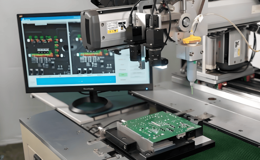
Professional contract manufacturers often maintain advanced quality systems. These systems typically include:
- Automated Optical Inspection (AOI)
- X-ray inspection for hidden joints
- Functional testing platforms
- Statistical process control
- Full production traceability
For regulated industries such as medical electronics or aerospace hardware, certifications are critical.
Quality-driven contract manufacturers often maintain certifications such as:
- ISO 9001
- ISO 13485
- IATF 16949
- AS9100
These certifications ensure that production processes meet strict industry standards. The OEM remains responsible for final product approval, but the manufacturing partner performs daily quality monitoring.
How to Choose Between Contract Manufacturer vs OEM?
Choosing the right model depends on the company’s business strategy, engineering capabilities, and production scale. Companies should evaluate several key factors before making a decision.
- 1. Product Development Capability
If your company has strong engineering resources, acting as the OEM and outsourcing production may be the best option. This approach allows full control over product innovation. If engineering capability is limited, partnering with OEM suppliers for subsystems may accelerate development.
- 2. Manufacturing Infrastructure
Building factories requires significant investment. Contract manufacturing eliminates the need for expensive production equipment. This model is especially attractive for startups and fast-growing technology companies.
- 3. Production Volume
High production volumes often benefit from specialized contract manufacturers. They already operate large-scale production lines optimized for efficiency. Low-volume projects may still benefit from outsourcing because setup costs remain manageable.
- 4. Time-to-Market Requirements
Launching products quickly can provide a competitive advantage. Contract manufacturers often reduce production ramp time. Their existing infrastructure allows faster manufacturing readiness.
- 5. Supply Chain Complexity
Electronics manufacturing involves complex supply chains. Experienced contract manufacturers maintain strong supplier networks. This can improve component availability and cost efficiency.
- 6. Quality and Compliance
Products in regulated industries require strict quality control. Selecting a manufacturing partner with proven certifications ensures compliance with industry standards. Ultimately, the choice is rarely absolute. Many successful companies operate as OEMs while relying heavily on contract manufacturers for production.
Conclusion:
Understanding the contract manufacturer vs OEM differences helps companies make smarter production decisions. An OEM focuses on product creation, intellectual property, and market strategy. A contract manufacturer specializes in efficient and reliable production.
For electronics companies seeking reliable PCB and PCBA production support, working with an experienced manufacturing partner can simplify the entire process.
Best Technology provides comprehensive PCB fabrication and PCBA assembly services for global customers. Our engineering teams support projects from prototype development to mass production, ensuring stable quality and rapid delivery.
If you are exploring manufacturing partnerships or planning a new electronics product, our team will be happy to help. Contact us at: sales@bestpcbs.com