PCB manufacturing PCB manufacturing
Home > Blog

Inductor Symbol Guide: Types, Meanings and Circuit Use

August 17th, 2026

An inductor symbol represents a component that stores energy in a magnetic field and opposes rapid changes in current. The familiar coil drawing identifies the component class, while added lines, arrows, taps and dots indicate its core, adjustability or magnetic coupling. Reading the drawing correctly is only the first step: a working PCB also needs the right inductance, current rating, DC resistance, self-resonant frequency, package and land pattern.

Inductor Symbol Guide: Types, Meanings and Circuit Use

What Is an Inductor Symbol?

The basic electrical inductor symbol is a series of curved loops between two terminals. It represents a conductive winding, not the exact number of turns or the component’s physical shape. A schematic may draw the loops horizontally or vertically without changing the electrical meaning. The reference designator normally starts with L, such as L1 or L203, and the inductance value is stated in henries, usually microhenries (uH) or nanohenries (nH) on PCB designs.

The symbol belongs to the logical schematic. It does not define whether the real component is a molded SMD power inductor, a small RF chip inductor, a common through-hole choke or a toroid. That physical decision is carried by the manufacturer part number, schematic properties, BOM and PCB footprint. A correct design keeps those records linked so that L1 cannot be assigned a symbol for one function and a land pattern for an incompatible package.

Why Is Inductance Represented by L?

Electrical schematics conventionally use L as the quantity and reference letter for inductance. The SI unit is the henry, written H. A value marked 10 uH beside L1 therefore means that the component’s nominal inductance is 10 microhenries; it does not describe its current capacity or resistance.

The voltage-current relationship is v = L di/dt. A larger inductance produces a larger voltage for the same rate of current change. Stored magnetic energy is W = 1/2 L I². These relationships explain why inductors smooth current in converters and filters, and why an interrupted inductive current can generate a large voltage transient. Real components also contain winding resistance, parasitic capacitance and core loss, so the ideal formula must be combined with datasheet limits.

How Does an Inductor Work in a Circuit?

Current through the winding creates magnetic flux. When the current changes, the changing flux induces a voltage that opposes that change. Under steady DC conditions, an ideal inductor eventually behaves like a short circuit. A real inductor retains its DC resistance and may heat from copper and core losses. At increasing frequency, inductive reactance rises according to XL = 2 pi fL until parasitic capacitance becomes significant near the self-resonant frequency.

In a buck converter, the inductor receives pulsed energy from the switching node and delivers a smoother current to the output. In an LC filter, it impedes high-frequency current while the capacitor diverts unwanted energy. In an RF matching network, a few nanohenries can tune impedance, but the pad geometry and nearby copper can contribute enough parasitic inductance and capacitance to alter the intended value.

Inductor symbol circuit examples in a buck converter and LC filter

What Are the Main Inductor Symbols?

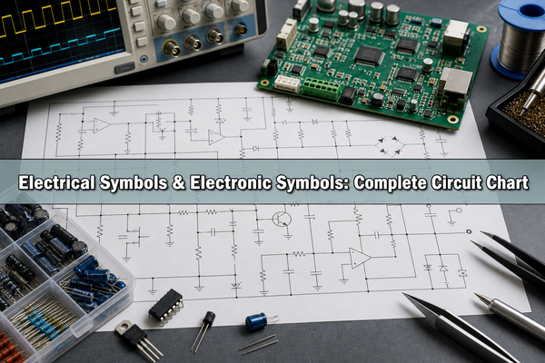
Most inductor symbols begin with the same coil form. Additional marks tell the reader what magnetic structure or electrical behavior matters in that circuit. The exact graphic style can vary between IEC, ANSI/IEEE and CAD libraries, so a project’s symbol legend and component properties remain authoritative.

Symbol type Typical graphic feature What it communicates
Fixed or air-core inductor Coil with no parallel core lines Fixed inductance; air core may be inferred when no magnetic-core mark is used
Iron-core inductor Coil beside two solid parallel lines Ferromagnetic iron or laminated core
Ferrite-core inductor Coil beside dashed parallel lines in many libraries Ferrite magnetic core
Variable inductor Diagonal arrow through or across the coil Adjustable inductance
Tapped inductor One winding with an intermediate terminal Electrical connection to part of the winding
Coupled inductors Two or more coils with core lines and often polarity dots Magnetic coupling and winding polarity

A schematic can also use specialized inductor symbols for saturable reactors, delay lines, current transformers or common-mode chokes. Do not select a component from the icon alone. Open its properties and check the description, part number, value, footprint and datasheet.

How Do Air-Core, Iron-Core and Ferrite-Core Symbols Differ?

An air-core symbol normally has no core lines. Air does not saturate like a ferromagnetic core and has low core loss, which can suit RF and high-frequency resonant circuits, but achieving high inductance generally requires more turns or a larger structure. The physical part may be an exposed helical coil even though the schematic only shows a generic winding.

An iron core inductor symbol usually adds two solid lines beside the coil. Iron or laminated steel cores are associated with lower-frequency magnetic components and energy storage where size and loss targets permit. A ferrite symbol often uses interrupted or dashed core lines. Ferrite materials have high electrical resistivity and are widely used in switching power, EMI suppression and high-frequency magnetics. Symbol conventions can differ across libraries, so the component description must state the actual core material.

Electrical inductor symbol comparison for air core iron core and ferrite core types

What Do Variable, Tapped, Coupled and Shielded Inductor Symbols Mean?

A diagonal arrow identifies a variable inductor. The adjustment may be mechanical, such as moving a core, and the datasheet defines its range and tuning method. A tapped symbol adds a terminal partway along one winding. The tap provides a selected turns ratio or impedance point, but it must not be mistaken for two independent windings.

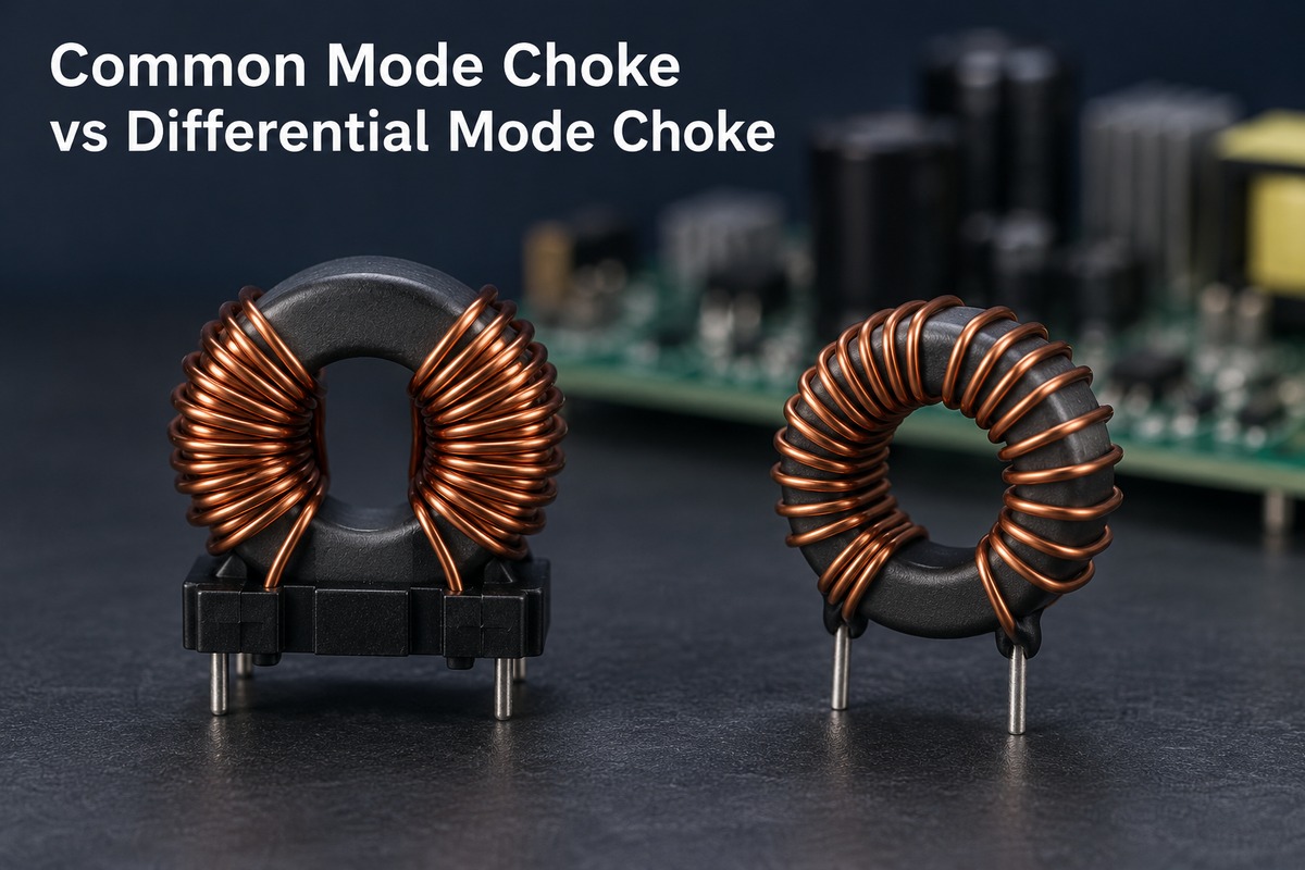
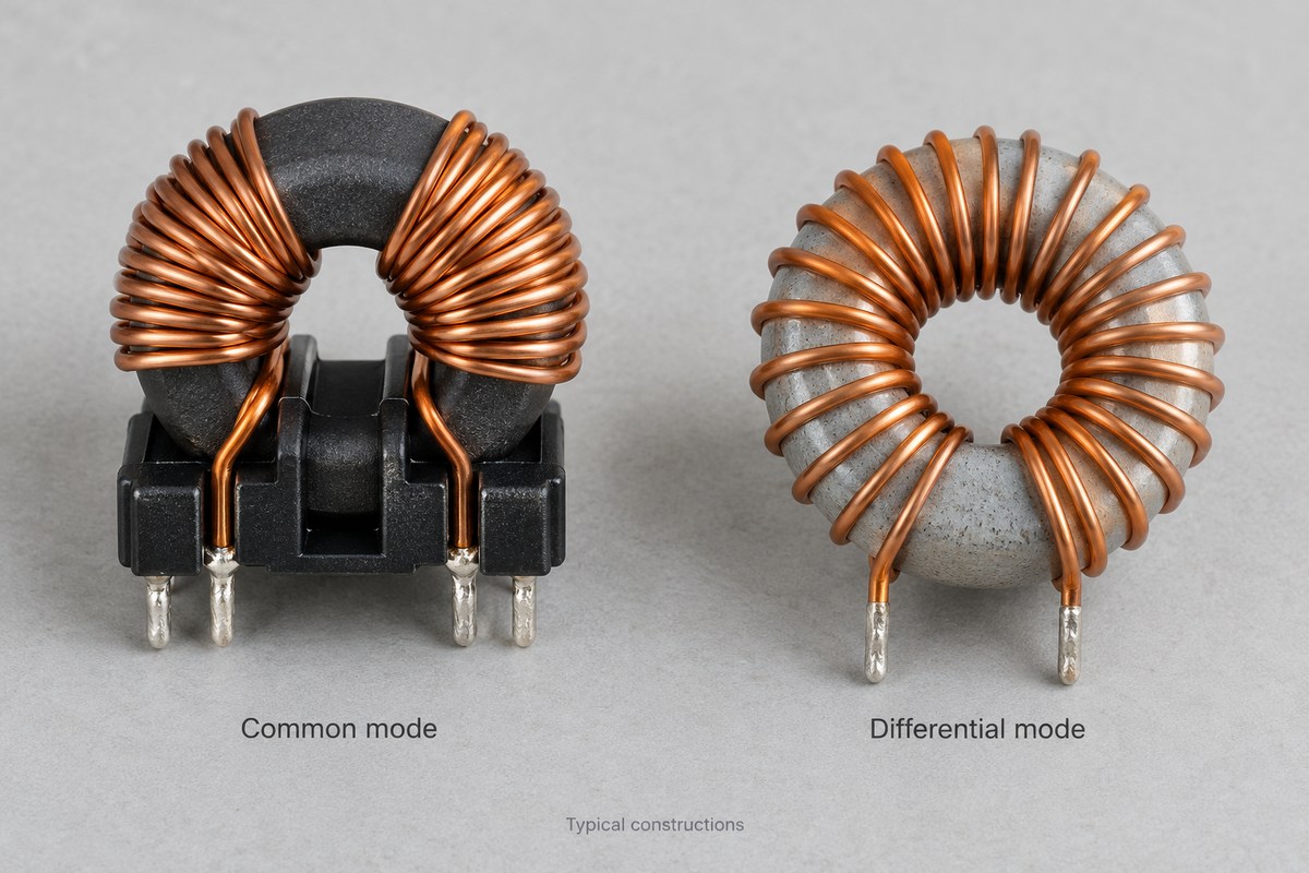
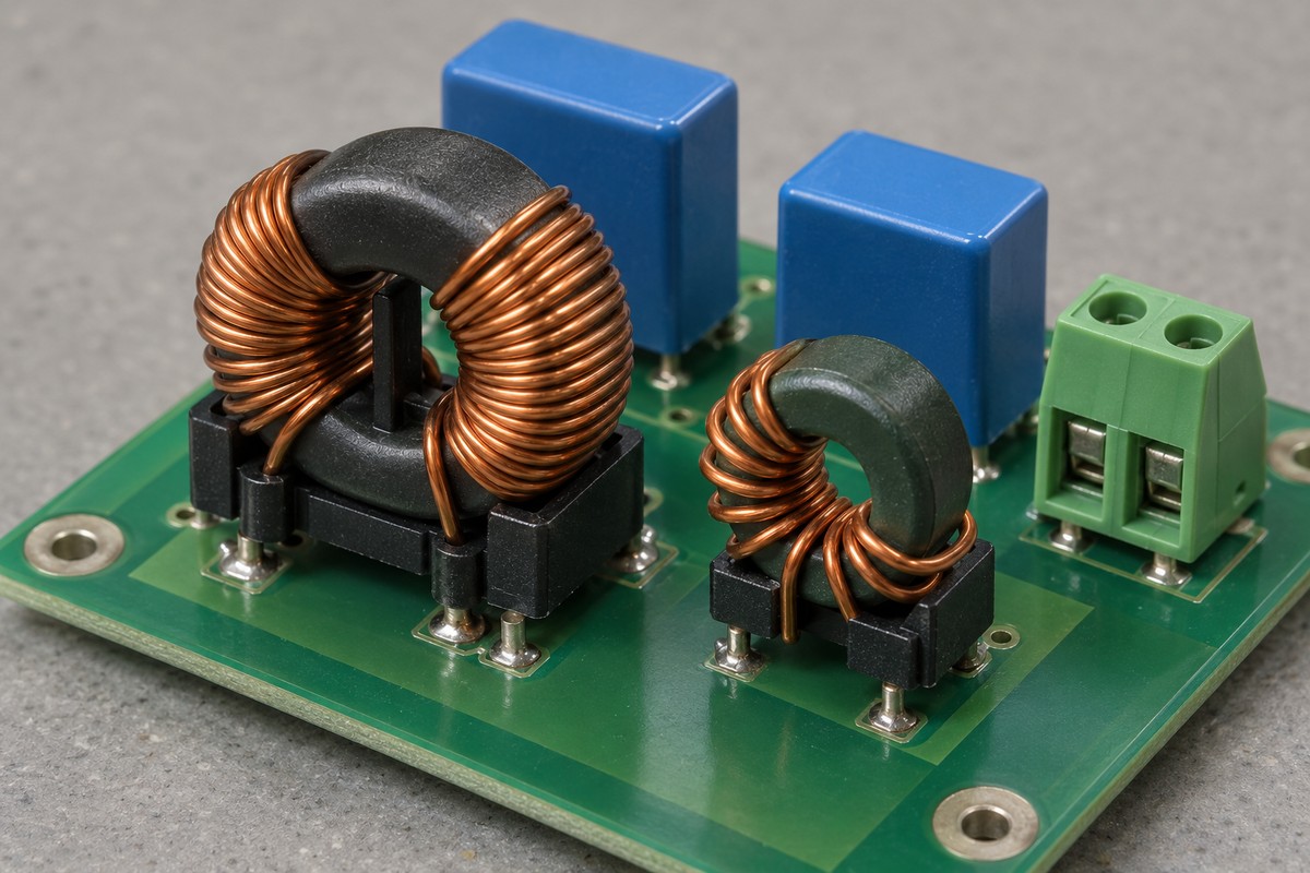
Coupled inductor symbols show two or more windings sharing magnetic flux. Polarity dots identify corresponding instantaneous winding polarity; reversing one winding changes the phase relationship and can prevent a converter or filter from operating correctly. A common-mode choke is a coupled component whose windings carry opposing signal currents while presenting high impedance to common-mode noise.

Shielding may be communicated by a dedicated library symbol, an enclosure mark, a part description or simply the selected manufacturer part. It is not represented identically in every schematic standard. The BOM should explicitly identify shielded or unshielded construction when radiated field, magnetic coupling or mechanical robustness matters.

Variable tapped coupled and shielded inductor symbols

How Do IEC and ANSI/IEEE Inductor Symbols Differ?

IEC 60617 provides an international database of graphical symbols for electrotechnical diagrams. ANSI/IEEE practices and individual CAD libraries may render the winding with semicircular loops, a compact curved line or a rectangular form. Core, tap and adjustability marks can also differ in spacing and orientation. These drawing differences do not change the underlying circuit behavior.

A project should use one approved symbol library rather than mixing graphics copied from unrelated sources. Each symbol needs a unique library name, correct pin count, visible reference designator, value field and verified footprint association. If a supplier drawing uses another convention, compare terminal numbers and winding polarity rather than judging equivalence by appearance.

How Do You Read an Inductor Symbol in a Circuit?

Start with connectivity, then inspect properties. In an inductor symbol circuit example, L1 might connect a switching node to an output capacitor, while L2 may sit in series with an RF signal or power input. The surrounding topology identifies the likely function more reliably than the coil icon by itself.

  1. Trace both terminals and identify the source, load, return path and nearby switching devices or capacitors.
  2. Read the reference designator, nominal inductance and tolerance.
  3. Open the BOM entry to confirm the manufacturer part number and approved alternatives.
  4. Check Isat, Irms, DCR, SRF, Q, operating temperature and core-loss data that apply to the circuit.
  5. Verify the footprint, pin numbering, orientation and assembly notes against the datasheet.

For a switching regulator, also compare the selected part with the controller vendor’s ripple-current calculation and transient requirements. For an RF circuit, evaluate the component model at the actual frequency; nominal inductance measured at a low test frequency may not predict its behavior close to self-resonance.

How Can You Distinguish Inductor, Transformer, Resistor and Capacitor Symbols?

A single coil is normally an inductor. Two or more closely aligned coils with a core and polarity marks often represent a transformer or coupled inductor; the circuit function and part description resolve the distinction. A resistor uses a zigzag or IEC rectangular symbol, while a capacitor uses two plates, with one curved plate or a polarity mark for certain polarized types.

Appearance alone is insufficient for multi-winding magnetics. A flyback transformer can resemble coupled inductors, while a common-mode choke can resemble a transformer. Terminal count, dot convention, turns ratio, isolation requirement and BOM description establish the actual component. Library names should use functional terms such as “common-mode choke, two-line” rather than a vague label such as “coil.”

What Information Does the Schematic Symbol Not Show?

The schematic symbol communicates electrical intent, but it usually omits the limits that determine whether the real inductor survives and performs correctly.

  • Inductance tolerance and bias behavior: inductance can decrease as DC current approaches saturation.
  • Isat and Irms: saturation current and thermal current are different ratings and may use different temperature-rise criteria.
  • DCR: winding resistance contributes conduction loss, voltage drop and temperature rise.
  • SRF and Q: parasitic capacitance limits the frequency range in which the component remains inductive.
  • Core loss: switching frequency, ripple waveform, flux swing and temperature affect magnetic loss.
  • Package and shielding: dimensions, termination style, magnetic shielding, weight and vibration behavior affect PCB implementation.

These parameters should reside in the approved BOM and design calculations. A substitution based only on equal microhenry value can increase loss, saturate during peak current, shift an RF network or fail the available PCB footprint.

How Should an Inductor Footprint Be Designed on a PCB?

Use the component manufacturer’s recommended land pattern as the starting point. Confirm pad dimensions, solder mask opening, paste coverage, courtyard, component height and pin-one or polarity information where applicable. For a heavy component, include mechanical clearance and consider shock, vibration and board flex. Do not enlarge pads casually: excessive solder can promote floating or tilt, while undersized pads can reduce joint reliability.

On a switching regulator, place the power inductor close to the switch, diode or synchronous MOSFETs and output capacitors specified by the topology. Keep the high di/dt loop compact, use copper widths suitable for current and avoid routing sensitive feedback or analog traces beneath an unshielded magnetic component. A conventional FR4 PCB can support many power and filtering applications when copper thickness, thermal rise and stack-up are verified.

High-frequency matching networks need tighter parasitic control. On an RF PCB, pad length, ground-via placement, trace width and component orientation can alter the effective inductance and impedance. Use the vendor’s S-parameter or equivalent-circuit model when available and keep the measured reference plane consistent with the PCB model.

How Are Inductors Assembled and Inspected on PCBs?

Most chip and molded power inductors use SMT reflow. Through-hole coils and toroids may use wave soldering, selective soldering or manual processes approved for the assembly. The thermal profile must respect the component’s termination, body material and moisture limits. Large thermal mass can change local solder behavior, and heavy parts may need adhesive or mechanical support for vibration environments.

Inspection should match the termination geometry. 3D solder paste inspection can verify paste before placement, AOI can check presence, offset, polarity marks and visible joints, and X-ray can support packages with hidden or difficult-to-see terminations. Electrical or functional testing is still needed to detect an incorrect value, open winding, saturation-related behavior or circuit-level noise that visual inspection cannot establish.

PCB assembly and inspection of SMD and through-hole inductors

EBest Circuit (Best Technology) supports SMT, THT and mixed PCB assembly, with minimum SMD capability down to 01005 and inspection options including 3D SPI, AOI, X-ray and functional testing. Maximum capability depends on the package, board dimensions, design complexity, quantity and engineering review; the selected inductor remains a component specified by its manufacturer datasheet.

Where Are Inductors Used?

Power converters use inductors to store energy and control ripple current. Input and output filters use them with capacitors to attenuate conducted noise. RF circuits use chip inductors in impedance matching, bias networks, resonators and filters. Common-mode chokes suppress noise on power, USB, Ethernet and other differential interfaces. Audio crossovers, sensors, wireless charging systems and motor drives use magnetic components for filtering, energy transfer or current control.

The application determines which parameter dominates. A power inductor emphasizes saturation current, thermal current, DCR and core loss. An RF inductor emphasizes Q, SRF, tolerance and a frequency-dependent model. An EMI choke emphasizes common-mode impedance, leakage inductance, insulation and line current. The schematic coil may look similar in every case, but the parts are not interchangeable.

FAQ About Inductor Symbols

What is the unit shown with an inductor symbol?

The SI unit is the henry (H). PCB schematics commonly use microhenries (uH) and nanohenries (nH). Always distinguish the value from the reference designator, such as L1.

Does an air-core inductor need a different symbol?

A coil without core lines is commonly used for a fixed or air-core inductor. Because libraries vary, the component description and part number should explicitly identify air-core construction when it matters.

What does the arrow across an inductor mean?

The arrow marks a variable or adjustable inductor. Its adjustment range and mechanism come from the datasheet, not from the arrow geometry.

What do dots beside coupled inductor symbols mean?

The dots mark corresponding winding polarity. Currents entering dotted terminals produce magnetic flux with the same reference polarity. Correct dot orientation is essential in coupled converters and transformers.

Can one symbol represent any inductor package?

Yes, one logical symbol can be reused across many packages, but each component record must link to the correct footprint and BOM part. A generic symbol never authorizes a generic footprint.

Conclusion

The inductor symbol identifies magnetic energy storage, while core lines, arrows, taps and polarity dots communicate specific behavior. Reliable hardware requires one more layer of checking: link the symbol to the correct value, datasheet limits, BOM part and physical footprint, then review placement, soldering and inspection for the actual circuit. For PCB fabrication or assembly support, contact EBest Circuit (Best Technology) at sales@bestpcbs.com.
You may also like

Multi Chip Module: Packaging, Design and PCB Integration

August 17th, 2026

A multi chip module places two or more semiconductor dies on a shared substrate so that the completed package can operate as one component. The approach can shorten critical connections, combine dies made with different processes and reduce the area required on the system board. Those benefits are not automatic: substrate technology, die attachment, power delivery, heat flow, test coverage and the PCB interface must be designed as one system.

Multi Chip Module: Packaging, Design and PCB Integration

What Is a Multi Chip Module?

A multi chip module, or MCM, is an electronic package or module containing multiple interconnected semiconductor dies. Logic, memory, analog, RF, sensor or power functions can share one package substrate. The module presents an external interface such as BGA balls, LGA lands or leads, allowing the system to handle it as a single component.

The defining point is the packaging hierarchy. Bare dies and their internal connections belong to the MCM. The larger board that receives the completed module is the system PCB. A board carrying several conventionally packaged ICs is a PCB assembly, but it is not automatically an MCM. Modern terminology overlaps with system-in-package and chiplet packaging, so the physical implementation and functional partition matter more than the label alone.

How Does a Multi Chip Module Work?

Each die performs a defined function and communicates through conductors in or on the shared substrate. Wire bonds can connect die pads to substrate pads. Flip-chip bumps can connect a die face-down to fine-pitch routing. An interposer or redistribution layer can provide much denser die-to-die paths than a conventional system PCB.

Multi chip module structure with bare dies package substrate BGA and system PCB

The substrate redistributes thousands of fine die connections to an external pitch that assembly equipment and the system PCB can support. It also carries power and ground, supports decoupling, controls impedance and provides part of the thermal path. Encapsulation, a lid, underfill or a heat spreader may protect the dies and stabilize the structure. The finished module is then soldered or mechanically connected to the system board.

What Are the Main Multi Chip Module Packaging Types?

Traditional multi chip module packaging is classified by how the interconnect substrate is made. MCM-L uses laminate technology, MCM-C uses ceramic processing and MCM-D uses deposited thin-film conductors and dielectrics. Modern packages may add silicon or organic interposers, redistribution layers, embedded bridges, fan-out structures or vertical stacking.

The class name does not fully define performance. A fine-line build-up laminate can outperform an older laminate construction, while a ceramic substrate may be chosen for dimensional or thermal reasons rather than maximum routing density. Die I/O pitch, signal speed, power density, module size, production volume and test strategy must be evaluated together.

How Do MCM-L, MCM-C and MCM-D Compare?

The practical decision starts with routing density, thermal expansion, heat flow and process maturity. The table summarizes the main differences without treating one technology as universally superior.

Type Substrate and process Typical strengths Primary constraints
MCM-L Organic laminate fabricated with advanced PCB or build-up processes Established supply chain, larger formats, practical multilayer routing and cost scaling CTE, moisture behavior, warpage and fine-feature limits depend on material and buildup
MCM-C Multilayer ceramic, commonly co-fired or thick-film processed Dimensional stability, electrical insulation, temperature capability and controlled material properties Higher material/process cost, brittle handling and shrinkage control
MCM-D Deposited thin-film metal and dielectric layers on a rigid base Fine routing, small vias and short high-performance interconnects Process complexity, equipment cost, layer buildup time and yield sensitivity
Comparison of MCM-L MCM-C and MCM-D multi chip module types

An MCM-L may use a multilayer FR4 PCB-like process when its electrical and thermal limits are appropriate. MCM-C can use a ceramic PCB or ceramic circuit substrate when insulation, dimensional stability or heat transfer justifies it. MCM-D is closer to thin-film microfabrication than ordinary PCB manufacturing.

What Is a Wafer Level Multi Chip Module?

A wafer level multi chip module uses wafer-level redistribution, fan-out or stacking processes to integrate multiple dies before the final package is completed. In a fan-out flow, known-good dies can be placed in a reconstituted wafer or panel, embedded in molding compound and connected with redistribution layers. Wafer-level system-in-package processes can place dies, passives or sensors side by side and can also support stacked configurations.

WMCM is not one fixed construction. The term may describe different multi-die wafer-level implementations, so package drawings must define die placement, redistribution layers, vertical connections, external ball pattern and thermal structure. It should not be used as a synonym for every MCM. The important distinction is that wafer-level processes form much of the package interconnect before singulation, unlike a laminate module assembled as an individual substrate.

What Matters in Multi Chip Module Design?

Multi chip module design is a chip-package-board co-design problem. Optimizing only die placement can leave an unrouteable substrate, an unstable power network or a poor thermal path. Start with the complete connectivity, power map, heat sources, package outline, external I/O and assembly constraints.

  • Die placement: keep high-bandwidth die pairs close, but reserve room for escape routing, decoupling, keepouts, underfill flow and heat spreading.
  • Signal integrity: control impedance, return paths, crosstalk, discontinuities and skew across die bumps, substrate routing, package balls and PCB traces.
  • Power integrity: size power/ground planes, place decoupling by frequency and current demand, and model simultaneous switching noise and voltage drop.
  • Thermal design: calculate die-level power maps rather than using only package-average power. Local hotspots can dominate junction temperature.
  • Mechanical design: review die size, substrate thickness, CTE mismatch, lid stiffness, underfill, molding and board attachment for warpage and fatigue.
  • Test access: plan die screening, boundary scan, package test, thermal monitoring and system diagnostics before routing is fixed.
Multi chip module electrical routing power delivery and thermal design

Short internal connections can reduce parasitic resistance, inductance and capacitance, but density also makes coupling and current concentration harder to control. Package and PCB models should therefore be analyzed together for fast interfaces. The same return-path discipline described in high-speed digital PCB design remains relevant after the signals leave the package.

How Is a Multi Chip Module Connected to a PCB?

The finished MCM commonly uses a BGA or LGA interface. Its ball or land map fans out into the system PCB through dog-bone vias, via-in-pad structures or microvias. The correct escape pattern depends on pitch, ball diameter, pad design, layer count, signal class, power distribution and assembly process. High-I/O modules can require an HDI PCB with laser-drilled microvias and sequential buildup.

The PCB stack-up must preserve return paths under high-speed signals, provide low-impedance power delivery and conduct heat away from the package. Thermal vias, internal copper planes, local copper density and a chassis or heatsink interface may all contribute. The board should also account for package warpage, component keepouts, rework clearance and the soldering profile.

Assembly data must identify package outline, pin-one orientation, paste stencil design, moisture sensitivity, reflow limits and inspection requirements. Very dense BGA interfaces usually need X-ray because optical inspection cannot see the internal solder joints.

How Do MCM, Chiplet, SiP and Monolithic IC Differ?

These terms describe different levels of integration. A chiplet is a die intended to be combined with other dies. An MCM is the package or module that interconnects multiple dies. A system-in-package usually emphasizes a complete system function and may include dies, passives, sensors, filters or MEMS. A monolithic IC integrates its functions on one die.

Term Physical meaning Design implication
Monolithic IC Functions fabricated on one semiconductor die Very short on-die links, but die size, process compatibility and yield constrain integration
Chiplet A modular die designed for multi-die integration Requires a defined die-to-die interface and compatible package architecture
MCM Multiple dies interconnected on a shared substrate or interposer Package-level electrical, thermal, mechanical and test co-design is essential
SiP Multiple functional elements combined as a packaged system May include MCM structures plus passives, sensors, RF filters or other components

The phrases multi chip module vs MCM do not describe competing technologies; MCM is simply the abbreviation. Multi chip module vs chiplet is different: the chiplet is one building block, while the MCM is an integration vehicle that may contain several chiplets or conventional dies.

Why Do MCM GPUs Support Continued Performance Scalability?

GPU and accelerator designs use multiple compute dies or chiplets to increase compute resources without making one monolithic die continually larger. Specialized dies for compute, cache, memory interfaces and I/O can be manufactured with process technologies suited to each function, then connected in an advanced package. This can improve design reuse and can reduce the yield penalty associated with a very large die.

Scalability still depends on the interconnect. Bandwidth, latency, synchronization, cache coherence, memory placement, package power and cooling determine whether additional dies deliver useful performance. AMD, for example, describes current accelerator architectures that connect GPU chiplets, high-bandwidth memory, cache and I/O through on-package Infinity Fabric links. The package does not remove the need for efficient workload partitioning or software support.

MCM GPU designs create a system tradeoff rather than a guarantee that adding dies will scale performance linearly. More dies can increase communication traffic and hotspot interaction, so architecture, packaging and cooling must advance together.

Where Are Multi Chip Modules Used?

Multi chip modules are used when several functions need a compact, high-bandwidth or application-specific connection. The implementation varies widely by industry.

  • High-performance computing: processors, GPUs, accelerators, cache and high-bandwidth memory packages.
  • RF and wireless: power amplifiers, switches, filters, control ICs and passive networks in compact front-end modules.
  • Automotive and industrial electronics: sensing, control, radar, power management and computing modules that require defined thermal and mechanical performance.
  • Medical and sensor systems: mixed-signal processing, sensing and communications integrated within a small package.
  • Aerospace and defense: dense computing or RF functions where size, weight, interconnect length and environmental qualification matter.

An intelligent power module may also integrate control and power semiconductor functions, but IPM and MCM are not interchangeable labels. The package construction, insulation structure, current path and thermal interface must be examined rather than inferred from the name.

What Can Go Wrong in Multi Chip Module Packaging?

Adding dies and interfaces creates more points that must be controlled. A design can be electrically correct and still fail because heat, stress, materials or test coverage were incomplete.

  • Known-good-die risk: one defective die can reduce the yield and value of an otherwise completed module.
  • CTE mismatch: silicon, organic laminate, ceramic, copper, molding compound and the system PCB expand differently during processing and operation.
  • Warpage: uneven materials, copper distribution or cure shrinkage can distort the substrate and disturb bump or BGA coplanarity.
  • Interconnect defects: non-wet joints, voids, opens, shorts, bond lift, bump fatigue and underfill voids may be hidden from optical inspection.
  • Electrical coupling: dense signal, power and ground structures can create crosstalk, return-path breaks, resonances and simultaneous switching noise.
  • Thermal interaction: one die can heat neighboring dies, while a package-average temperature hides a local hotspot.

Reliability is therefore conditional. Shorter connections can reduce some parasitics and board-level joints, but an MCM does not automatically outlast a single-die package. Material characterization, simulation, controlled assembly and qualification determine the result.

How Are Multi Chip Modules Inspected and Tested?

Inspection should follow the structure from die to system board. Wafer probing and known-good-die screening reduce the chance of packaging defective silicon. During module assembly, optical inspection can verify placement and wire bonds, while X-ray can reveal hidden bumps, BGA joints, bridges, opens and void patterns. Scanning acoustic microscopy may be used to detect delamination or underfill defects.

X-ray inspection of a multi chip module mounted on a PCB

Electrical tests include continuity, shorts, parametric checks and functional operation. Boundary scan can improve access when physical probing is limited. Thermal cycling, temperature-humidity, high-temperature operating tests, mechanical stress and power cycling are selected according to the application and dominant failure mechanisms. At the system-board level, PCB assembly controls such as solder paste inspection, AOI, X-ray and functional testing verify the module-to-board interface. The existing guide to X-ray inspection in PCB assembly explains the value of hidden-joint imaging in more detail.

What Should Multi Chip Module Manufacturers Coordinate with PCB and PCBA Teams?

Multi chip module manufacturers and system-board teams must exchange interface data early. The package outline, ball map, pin functions, pitch, pad recommendation, allowed via structures, power map, thermal resistance model, warpage limit, moisture classification and reflow window affect PCB layout and assembly. Signal models and power-delivery models are needed when the module carries fast interfaces or high transient current.

The PCB team should return the proposed stack-up, fan-out geometry, impedance targets, plane assignment, thermal-via design and mechanical constraints. The assembly team should confirm stencil strategy, paste type, placement support, reflow profile, X-ray criteria, cleaning limits and rework access. Revision control is critical: a changed ball assignment or package drawing can invalidate both layout and test fixtures.

EBest Circuit (Best Technology) supports the PCB and PCBA side of this integration. Published capabilities include HDI line/space down to 2/2 mil, HDI holes down to 0.10 mm and BGA pitch down to 0.25 mm. Maximum capability depends on material, layer stack-up, board dimensions, design complexity, production quantity and engineering review. These capabilities do not mean EBest Circuit fabricates semiconductor dies or wafer-level MCM packages; the scope is the supporting PCB, ceramic circuit and board-level assembly work.

FAQ About Multi Chip Modules

Is a multi chip module the same as a chiplet?

No. A chiplet is a modular die. A multi chip module is the package or assembly that interconnects multiple dies; it may contain chiplets, conventional dies or both.

Is MCM the same as multi chip module?

Yes. MCM is the standard abbreviation for multi chip module. The exact physical construction still needs to be defined because MCM-L, MCM-C, MCM-D and wafer-level designs use different processes.

Can a multi chip module use both wire bonding and flip chip?

Yes. A heterogeneous module can use different attachment methods for different dies when the substrate layout, assembly sequence, wire clearance, underfill and thermal process are compatible.

What does “MCM GPU multi chip module GPUs for continued performance scalability” mean?

It refers to partitioning a GPU or accelerator across multiple compute, cache, memory or I/O dies and connecting them in one advanced package. Continued performance scaling depends on die-to-die bandwidth, latency, power, cooling and software efficiency, not only the number of dies.

Is wafer level multi chip module packaging the same as MCM-L?

No. MCM-L is based on a laminate substrate. Wafer-level multi-die packaging typically uses redistribution, fan-out, molding or stacking processes formed at wafer or panel scale before final singulation.

Can a finished MCM be assembled on a standard PCB?

Sometimes. The external pitch, I/O count, power, thermal load and signal speed determine whether a conventional multilayer board is sufficient or an HDI, high-frequency or ceramic solution is required.

Conclusion

A multi chip module can combine specialized dies, shorten internal connections and reduce system-board area, but its value depends on coordinated package, thermal, test and PCB design. MCM-L, MCM-C, MCM-D and wafer-level approaches solve different density, material and manufacturing problems. When a completed module needs an HDI, FR4 or ceramic system board and controlled PCBA integration, EBest Circuit (Best Technology) can review the PCB-side construction and assembly requirements. Contact sales@bestpcbs.com.
You may also like

0603 Resistor Power Rating: Wattage, Derating and Limits

August 7th, 2026

The 0603 resistor power rating is commonly around 0.1 W, or 100 mW, for many general-purpose thick-film resistors. That figure is a useful reference, but it is not a universal limit for every 0603 component. The usable wattage depends on the resistor series, construction, resistance value, maximum working voltage, temperature, pulse conditions, and PCB thermal environment.

A reliable design therefore requires more than checking whether a simple power calculation falls below 0.1 W. The 0603 resistor power rating must be considered together with temperature derating, working-voltage limits, pulse capability, and design margin. This article explains how to make those checks and when a standard 0603 should be replaced with a higher-power part, a larger package, or a resistor network.

0603 Resistor Power Rating, https://www.bestpcbs.com/blog/2026/08/0603-resistor-power-rating/

What Is the Typical Power Rating of a 0603 Resistor?

For many general-purpose thick-film products, the typical 0603 resistor power rating is approximately 0.1 W, equal to 100 mW or 1/10 watt. However, 0603 identifies the package size rather than a fixed electrical rating.

An imperial 0603 resistor has nominal dimensions of about 0.06 × 0.03 inch, corresponding to roughly 1.6 × 0.8 mm. Different resistor technologies can occupy the same footprint while carrying different wattage ratings.

0603 Resistor TypeTypical Power Rating
General-purpose thick filmAround 0.1 W
Precision thin film0.063–0.1 W
Lower-power series0.063–0.075 W
Enhanced-power 06030.125 W or higher
High-power 06030.15–0.2 W or higher
Current-sense 0603Series-dependent
Pulse-resistant 0603Series-dependent

The exact 0603 resistor power rating must come from the selected component datasheet because package size alone does not define wattage.

0603 resistor, https://www.bestpcbs.com/blog/2026/08/0603-resistor-power-rating/

Why Do Different 0603 Resistors Have Different Power Ratings?

Two 0603 resistors can have the same external dimensions and very different continuous power capabilities. The difference comes mainly from how the resistive element generates, spreads, and transfers heat.

The main factors are:

  • Resistive material: Thick-film, thin-film, metal-element, and other technologies have different thermal behavior and allowable element temperatures.
  • Element geometry: The shape and thickness of the resistive path influence current density and local hot spots.
  • Ceramic substrate: The substrate helps move heat from the resistive element toward the terminations.
  • Termination construction: End terminations provide a major thermal path from the component into the solder pads and PCB copper.
  • Maximum element temperature: Different product families are designed to tolerate different internal temperatures.
  • Qualification conditions: Published power can depend on specified pad dimensions, PCB construction, copper area, ambient temperature, or terminal temperature.

This matters when one resistor is substituted for another. Two parts listed as 10 kΩ, 1%, 0603 may fit the same footprint but still differ in wattage, voltage capability, temperature behavior, and pulse performance.

For a power-sensitive position, compare the 0603 resistor power rating, maximum working voltage, derating characteristics, pulse capability, operating-temperature range, and TCR before approving a substitute.

How Do You Read a 0603 Resistor Power Rating from a Datasheet?

A datasheet should be treated as an operating envelope, not as a single wattage number. Seeing “0.1 W” in a specification table is only the first step.

Datasheet ParameterTechnical Significance
Rated PowerContinuous allowable dissipation
Reference TemperatureTemperature at which full rated power applies
Derating CurveReduction in allowable power at elevated temperature
Maximum Working VoltageHighest permitted continuous voltage
Overload VoltageShort-duration electrical stress limit
Operating TemperaturePermitted operating temperature range
Pulse SpecificationAllowable pulse power or energy
TCRResistance variation with temperature

First, confirm that the value belongs to the 0603 package or metric 1608 equivalent. Datasheets often place 0402, 0603, 0805, and 1206 values next to one another, so using the wrong row can lead to an incorrect design limit.

Next, identify the thermal condition associated with the published 0603 resistor power rating. A resistor may support full rated power only up to a specified ambient or terminal temperature. Above that point, the available wattage falls according to the derating curve.

Then check the maximum working voltage separately. A high-resistance 0603 resistor can dissipate relatively little power while still exceeding its allowable continuous voltage.

Before approving the part, verify:

  • Rated power at the actual operating temperature
  • Maximum continuous working voltage
  • Short-duration overload limits
  • Pulse or surge capability
  • Operating-temperature range
  • Any mounting conditions stated in the datasheet

The component is suitable only when all applicable limits are satisfied at the same time.

How Do You Calculate Power Dissipation for a 0603 Resistor?

The electrical load should be calculated before comparing the circuit with the 0603 resistor power rating.

The standard relationships are:

P = V × I

P = I² × R

P = V² ÷ R

where:

  • P = power in watts
  • V = voltage across the resistor
  • I = current through the resistor
  • R = resistance in ohms

Consider a 1 kΩ resistor with 5 V across it:

P = 5² ÷ 1000 = 0.025 W

The resistor dissipates 25 mW. For a resistor nominally rated at 0.1 W, that is 25% of the nominal rating before temperature derating is applied.

Now place 10 V across the same 1 kΩ resistor:

P = 10² ÷ 1000 = 0.1 W

The dissipation rises to 100 mW, equal to the nominal rating of many standard 0603 resistors.

The key relationship is that, with a fixed resistance, power rises with the square of voltage. Doubling the voltage from 5 V to 10 V increases resistor dissipation by four times.

A practical calculation should include:

  • Maximum supply voltage: Use the highest credible operating voltage, not just the nominal rail value.
  • Resistance tolerance: Select the tolerance extreme that produces the highest stress in the actual circuit.
  • Maximum continuous current: Typical current may underestimate thermal load.
  • Startup and shutdown conditions: Some circuits expose resistors to higher stress before steady-state operation begins.
  • Fault conditions: Include abnormal states when the resistor is expected to survive them.
  • Duty cycle: Switched loads require both peak and average power to be considered.

After calculating the worst-case value, compare it with the temperature-derated 0603 resistor power rating, not only the room-temperature value.

0603 resistor power dissipation, https://www.bestpcbs.com/blog/2026/08/0603-resistor-power-rating/

How Do Resistance Value and Maximum Working Voltage Limit 0603 Resistor Power?

Power and voltage limits are related, but they are not interchangeable. A resistor can remain below its thermal limit while already exceeding its permitted working voltage.

For a given resistance and power, the theoretical voltage is:

V = √(P × R)

Using a nominal 0.1 W power limit:

ResistanceVoltage at 0.1 W
100 Ω3.16 V
1 kΩ10 V
10 kΩ31.6 V
100 kΩ100 V
1 MΩ316 V

These are mathematical power values, not guaranteed safe working voltages.

For example, a 1 MΩ resistor mathematically reaches 0.1 W at approximately 316 V. If the selected 0603 series has a maximum working voltage far below 316 V, the voltage specification becomes the limiting factor long before the 0603 resistor power rating is reached.

In practice:

  • Low-resistance values: Current and thermal dissipation are more likely to become limiting factors.
  • High-resistance values: Maximum working voltage may become the dominant constraint.

This distinction matters in high-voltage dividers, DC bus sensing, capacitor discharge networks, battery monitoring, high-impedance measurement paths, and power-supply feedback circuits.

If one resistor cannot meet the required voltage and wattage simultaneously, a series network can distribute both voltage and dissipation. PCB creepage and clearance still have to meet the total circuit-voltage requirements.

How Does Temperature Derating Affect the 0603 Resistor Power Rating?

The nominal 0603 resistor power rating normally applies only within a defined temperature range. Above the manufacturer’s reference temperature, the allowable continuous power decreases.

This reduction is called power derating.

Suppose, purely as an example, that a 0.1 W resistor permits full power up to 70°C and then derates linearly to zero at 155°C.

At 100°C:

Remaining power ratio = (155 − 100) ÷ (155 − 70) = 64.7%

The allowable continuous dissipation would be:

0.1 W × 64.7% = 64.7 mW

The temperatures in this example are illustrative rather than universal. The correct values must come from the selected resistor series.

The practical lesson is simple: a nominal 100 mW resistor may no longer support 100 mW once the PCB becomes hot.

Local temperature can rise because of:

  • MOSFETs and regulators: Heat spreads through nearby PCB copper.
  • Power inductors and transformers: Magnetic components often create concentrated hot areas.
  • High-power LEDs: Their thermal load can raise the surrounding board temperature.
  • Closely spaced loaded resistors: Several moderate heat sources can combine into one local hot spot.
  • Sealed enclosures: Restricted convection increases internal PCB temperature.
  • Elevated ambient conditions: Outdoor, automotive, industrial, and enclosed electronics may operate far above room temperature.

When the 0603 resistor power rating is being used close to its limit, base derating on the temperature seen by the resistor during real operation, not simply on room temperature.

How Do PCB Layout and Thermal Conditions Affect 0603 Resistor Power Handling?

A surface-mount resistor transfers much of its heat through the end terminations and solder joints into the PCB. That makes the board part of the resistor’s thermal environment.

Several layout choices can influence operating temperature:

  • Pad geometry: A suitable land pattern provides a predictable electrical, mechanical, and thermal connection.
  • Connected copper area: Wider copper regions can spread heat more effectively than narrow traces.
  • Copper thickness: Additional copper can improve local heat spreading where the circuit permits it.
  • Thermal vias: In suitable layouts, vias can transfer heat toward internal planes or the opposite side of the board.
  • Component spacing: Separating loaded resistors from MOSFETs, regulators, inductors, and LEDs reduces thermal coupling.
  • Airflow: Natural or forced airflow changes how quickly heat leaves the PCB surface.
  • Internal copper planes: Large connected copper areas can alter the local thermal path and board temperature.

One issue that is easy to miss is thermal accumulation. A single resistor dissipating moderate power may remain within limits. Put ten similarly loaded resistors into the same small area, however, and the surrounding PCB can become considerably warmer.

Thermal testing deserves particular attention when:

  • Several resistors dissipate meaningful continuous power
  • The PCB operates inside a sealed enclosure
  • Power semiconductors are located nearby
  • The calculated load approaches the derated limit
  • Prototype temperatures differ from thermal estimates

PCB layout can help control temperature, but it should not be used to redefine the manufacturer’s 0603 resistor power rating.

How Much Power Margin Should You Use for a 0603 Resistor?

There is no universal rule requiring every 0603 resistor to operate at exactly 50%, 60%, or another fixed percentage of its rating.

A useful margin depends on the worst-case load, actual temperature, component tolerances, transient conditions, and required service life.

For example, a 0.1 W resistor dissipating 40 mW uses 40% of its nominal rating. A resistor dissipating 80 mW uses 80%. That comparison is meaningful only before temperature derating is applied.

If the actual PCB temperature reduces the allowable wattage to 65 mW, then an 80 mW load is already outside the permitted range even though it is below the nominal 100 mW value.

When deciding how much margin is enough, consider:

  • Worst-case continuous dissipation: Base the calculation on the highest credible normal voltage or current.
  • Derated allowable power: Compare the actual load with the rating available at the real operating temperature.
  • Supply tolerance: A modest increase in voltage can create a much larger increase in resistor power.
  • Resistance tolerance: Component variation can affect current and dissipation depending on the circuit.
  • Startup and transient behavior: Short periods of additional loading should not be ignored.
  • Local temperature: Heat from neighboring components can reduce the remaining margin.
  • Expected operating life: Continuous high temperature leaves less room for aging and long-term drift.

Some designs use 50% of nominal power as an internal derating target, but that is a project rule rather than a universal standard.

A better rule is to keep worst-case continuous dissipation comfortably below the temperature-derated 0603 resistor power rating under actual operating conditions.

How Much Pulse or Surge Power Can a 0603 Resistor Handle?

A short pulse can sometimes exceed the continuous 0603 resistor power rating because the event ends before the entire resistor reaches thermal equilibrium.

That does not mean pulse capability can be estimated by multiplying the continuous wattage by an arbitrary factor.

Four variables are especially important:

  • Pulse duration: A 10 µs event and a 100 ms event at the same peak power create very different thermal stresses.
  • Peak voltage and current: Instantaneous electrical stress must remain within the applicable pulse limits.
  • Pulse energy: Energy deposited during the event influences localized heating and element damage.
  • Repetition rate: Frequent pulses may not leave enough cooling time between events.

For repetitive pulses, average power also matters:

Average power = energy per pulse × pulse repetition frequency

A resistor may therefore survive a single startup event but fail when the same pulse occurs hundreds or thousands of times per second.

Pulse capability deserves close attention in gate-drive circuits, snubber networks, capacitor charging and discharge paths, inrush circuits, switching converters, surge-sensing networks, and motor-control electronics.

A standard 0.1 W resistor and a pulse-resistant 0.1 W resistor can behave very differently under short overloads. For pulsed operation, check the pulse-load curve, overload specification, or energy limit for the exact resistor series rather than relying on the continuous 0603 resistor power rating.

How Do Standard and High-Power 0603 Resistors Differ?

A high-power 0603 resistor is intended to provide more continuous dissipation within approximately the same 1.6 × 0.8 mm footprint.

That makes it attractive when PCB space is tight, but higher wattage does not automatically make it the better part for every application.

ParameterStandard 0603High-Power 0603
Continuous PowerUsually lowerHigher
Package Size06030603
Thermal CapabilityConventionalEnhanced
Working VoltageSeries-dependentSeries-dependent
Pulse CapabilitySeries-dependentSeries-dependent
Tolerance / TCRProduct-dependentProduct-dependent
CostUsually lowerOften higher

A high-power version is most useful when:

  • Board area cannot increase, but more continuous power margin is required.
  • Normal operating dissipation is too close to the derated limit of a standard part.
  • The PCB runs warm, and a resistor series with a more suitable thermal specification is available.
  • The higher-power part still meets the required resistance, tolerance, TCR, voltage, and availability requirements.

It is less helpful when another parameter is causing the problem:

  • Excess working voltage: Higher wattage does not automatically mean a higher voltage rating.
  • Severe pulses: A dedicated pulse-resistant resistor may be the better choice.
  • Precision requirements: Higher rated power does not guarantee lower TCR, lower noise, or better long-term stability.
  • Environmental requirements: Automotive, anti-sulfur, humidity, and other qualifications remain independent specifications.

The 0603 resistor power rating is only one part of the selection decision. Identify the real limiting parameter before paying for a higher-power component.

How Does 0603 Power Rating Compare with 0402, 0805 and 1206 Resistors?

Larger resistor packages usually support more conventional continuous power because they provide a larger body and thermal path into the PCB.

PackageApprox. Metric SizeCommon General-Purpose Power
04021.0 × 0.5 mmAround 0.063 W
06031.6 × 0.8 mmAround 0.1 W
08052.0 × 1.25 mmAround 0.125 W
12063.2 × 1.6 mmAround 0.25 W

These values are representative rather than guaranteed ratings. Specialized resistor families can differ substantially.

The package choice affects more than wattage:

  • 0402: Useful where board density is critical and resistor dissipation is very low.
  • 0603: Offers a practical balance of compact size, availability, assembly handling, and moderate power.
  • 0805: Provides more thermal headroom with only a moderate increase in board area.
  • 1206: Offers significantly more physical area where higher dissipation is required and space is available.

The 0603 vs 0805 power rating decision becomes particularly relevant when a standard 0603 is already close to its usable thermal limit. In that situation, moving to an 0805 may be simpler and more robust than operating a specialized 0603 near its maximum 0603 resistor power rating.

Working voltage and pulse ratings should still be checked separately because package size alone does not define every electrical limit.

0603 Resistors, https://www.bestpcbs.com/blog/2026/08/0603-resistor-power-rating/

When Should You Replace a 0603 Resistor with a Larger Package or Multiple Resistors?

A 0603 resistor deserves reconsideration when its electrical and thermal margins become narrow under worst-case conditions.

Moving to 0805 or 1206 is often the simplest option when:

  • Continuous dissipation approaches the derated 0603 limit.
  • The PCB remains hot during normal operation.
  • Long service life favors a lower component temperature.
  • Available 0603 products do not provide enough working-voltage capability.
  • Pulse conditions exceed the capability of suitable 0603 resistor families.
  • Several limits are being approached at the same time.

A resistor network is another option.

Series resistors are useful when voltage is the primary constraint. They divide the total resistance, voltage, and power across several components.

Parallel resistors can distribute current and thermal dissipation when one component would otherwise carry too much load.

That approach introduces its own design considerations:

  • Resistance tolerance: Electrical stress may not divide exactly as expected.
  • TCR variation: Sharing can change as individual resistors heat.
  • Unequal PCB temperature: Two nominally identical parts can operate differently when one sits closer to a heat source.
  • Copper geometry: Layout affects both current distribution and temperature.
  • Additional solder joints: More parts mean more placements and interconnections.

The best solution may be a high-power 0603, an 0805 or 1206 resistor, a series network, or a parallel network. The choice should follow the actual limiting parameter and the required 0603 resistor power rating margin rather than package preference alone.

What Causes a 0603 Resistor to Overheat, Drift or Fail on a PCB?

An overloaded resistor does not always burn or go open-circuit immediately. Prolonged electrical or thermal stress may first appear as resistance drift, unstable readings, discoloration, localized heating, or intermittent operation.

Common causes include:

  • Excess continuous power: Higher-than-expected voltage or current can push dissipation above the allowable 0603 resistor power rating. Measure the real voltage across the component and calculate its actual load.
  • Insufficient temperature derating: A resistor that works at room temperature may become overstressed once the PCB heats up. Check the local operating temperature, not only ambient room temperature.
  • Excess working voltage: High-value resistors can exceed their voltage limit while still dissipating relatively little power.
  • Pulse or surge overload: Switching circuits may expose the resistor to short but severe electrical stress. Examine pulse width, peak voltage, peak current, energy, and repetition rate.
  • Thermal accumulation: Several loaded resistors or nearby power components can raise the temperature of the same PCB area.
  • Incorrect resistor value: A BOM error or incorrect substitute can change circuit current enough to raise dissipation dramatically.
  • Poor solder joints or excessive rework: Damaged terminations or weak joints can affect both electrical reliability and heat transfer.
  • PCB flexure: Mechanical bending can crack the ceramic body, damage terminations, or weaken solder joints.
  • Unsuitable environmental rating: Moisture, corrosive gases, sulfur compounds, contamination, and thermal cycling can gradually affect a resistor that was not selected for those conditions.

When a 0603 resistor repeatedly runs hot or fails, replacing it with the same part is not a root-cause fix. Measure the real electrical load and local temperature first, then compare those values with the resistor’s voltage, pulse, and derated power limits.

FAQs About 0603 Resistor Power Rating

Q1: Is a 0603 resistor the same as a 1608 resistor?

A1: Yes. Imperial 0603 corresponds approximately to metric 1608, which represents a body size near 1.6 × 0.8 mm. The two naming systems use different numbering conventions, so package codes should not be interpreted in the same way. Confirm the actual dimensions when selecting a footprint or substitute.

Q2: Are 0603 resistors polarized?

A2: No. A conventional 0603 chip resistor is non-polarized, so either electrical orientation provides the same basic resistance function. Production may still standardize orientation for inspection consistency or documentation, but reversing the component does not reverse its electrical behavior.

Q3: Can a 0603 resistor be used in an AC circuit?

A3: Yes, provided the resistor remains within its RMS power, peak-voltage, and frequency-related limits. For a sinusoidal waveform, heating is normally evaluated using RMS voltage or current. Higher-frequency circuits may require additional consideration of parasitic impedance.

Q4: Does frequency affect the resistance of a 0603 resistor?

A4: At low frequencies, a chip resistor behaves close to its nominal resistance. At higher frequencies, parasitic inductance and capacitance affect impedance. RF, microwave, and high-speed applications may therefore require resistor families with specified high-frequency performance.

Q5: Can a 0603 resistor be used as a fuse?

A5: A standard 0603 resistor should not be assumed to provide controlled fuse behavior. Its failure mode, opening time, and overload response are not defined like those of a purpose-designed fuse or fusible resistor. If predictable circuit protection is required, use a component specifically rated for that function.

Q6: What resistance values are available in the 0603 package?

A6: The available range depends on resistor technology and product family. General-purpose 0603 products cover a very broad resistance range, while precision, current-sense, high-value, or specialized parts may cover narrower ranges. The exact range should be confirmed for the selected series.

Q7: Do 0603 resistors have printed resistance codes?

A7: Many modern 0603 resistors have no readable top marking because the package is very small. Some product families may use abbreviated markings, but these are not enough to identify every electrical specification. The manufacturer part number and BOM remain the reliable references.

Q8: Can a multimeter measure a 0603 resistor while it is still on the PCB?

A8: It can, but an in-circuit reading may be influenced by parallel resistive paths, semiconductor junctions, capacitors, or other connected components. If the measured value does not match expectations, lifting one terminal or removing the resistor may be required for an accurate standalone measurement.

Q9: Can 0603 resistors be mounted on either side of a PCB?

A9: Yes. They can be assembled on the top or bottom side provided the PCB assembly process supports the selected placement and reflow sequence. Placement should still consider clearance, inspection access, nearby components, and the board’s mechanical environment.

Q10: Are 0603 resistors suitable for automated SMT assembly?

A10: Yes. The 0603 package is widely used in automated pick-and-place and reflow assembly. Proper land patterns, solder paste deposition, placement accuracy, and reflow control help maintain consistent solder joints and reduce defects such as tombstoning.

Q11: Can a 0603 resistor be used as a pull-up or pull-down resistor?

A11: Yes. Pull-up and pull-down functions generally dissipate relatively little power, making the 0603 package suitable for many digital circuits. The resistance value should be selected according to logic level, leakage current, switching speed, and required bias current rather than wattage alone.

Q12: What resistor tolerances are commonly available in 0603 packages?

A12: Common 0603 resistor families are available in tolerances such as 5%, 1%, 0.5%, 0.1%, and tighter values depending on the technology. Tighter tolerance does not automatically mean a higher 0603 resistor power rating; precision and power capability are separate specifications.

Q13: Is a 0603 resistor electrically different from a 0603 capacitor?

A13: Yes. The shared “0603” designation refers only to the approximate package dimensions. A resistor provides resistance, while a capacitor stores electrical charge and has capacitance, voltage, dielectric, and frequency characteristics. Identical package codes do not indicate equivalent electrical functions.

The 0603 resistor power rating is commonly around 0.1 W, but reliable component selection requires more than matching a resistor to that single number. The finished design must keep the component within its continuous power, working-voltage, temperature-derating, and pulse limits under the actual PCB operating conditions.

Calculate worst-case dissipation first, then check the result against the resistor’s usable power at the expected temperature. When the available 0603 resistor power rating margin becomes narrow, a high-power 0603, larger 0805 or 1206 package, or properly designed resistor network can provide a more robust solution than running a standard part close to its limit.

If your project involves power-sensitive resistor networks, high-voltage sensing, compact PCB layouts, prototype development, or PCB assembly, we can support PCB fabrication and PCBA production from prototype through volume manufacturing.

Send your Gerber files, BOM, assembly requirements, and order quantity to EBest Circuit sales@bestpcbs.com to request a technical review and PCB/PCBA quotation.

You may also like

FPGA Vendors: Selection Guide for PCB and PCBA Projects

August 6th, 2026

Choosing FPGA vendors are not simply a comparison of logic cells, speed, and unit price. The selected platform also determines the toolchain, IP licenses, package, power rails, BGA fanout, PCB layer count, sourcing options, and production-test method.

A device may meet the functional specification yet still increase PCB cost or create a supply problem. Before fixing the part number, compare the exact device, package, lifecycle, purchasing channel, and manufacturing impact.

FPGA vendors

Which Major FPGA Vendors Should Be Shortlisted?

The right shortlist depends on the application. A high-speed networking project, compact industrial controller, low-power sensor, and long-life aerospace product will not use the same selection logic.

FPGA vendorTypical fitPCB concern
AMDBroad portfolio, high-speed and adaptive computingDense BGA, power rails, transceivers
AlteraIndustrial, embedded and high-performance platformsTool edition, package and bank planning
LatticeCompact, low-power control and edge applicationsI/O capacity and package limits
MicrochipIndustrial, security and long-lifecycle projectsProgramming and device availability
AchronixHigh-bandwidth acceleration and networkingPower, memory and high-speed routing
EfinixVision, edge and compact embedded systemsFine-pitch BGA and HDI risk
GOWINCost-sensitive embedded applicationsTool support and approved sourcing

A practical shortlist normally contains two or three exact devices. Comparing every vendor adds work without improving the final decision.

FPGA vendors

Which FPGA Vendor Selection Criteria Prevent a PCB Redesign?

Start with mandatory requirements. A device that fails one essential condition should be removed before PCB design begins.

Check:

  • Logic, DSP and RAM capacity
  • Required speed and temperature grade
  • Available user I/O
  • I/O-bank voltage compatibility
  • Memory and transceiver support
  • Package size and ball pitch
  • Power rails and sequencing
  • Tool and IP availability
  • Lifecycle status
  • Approved purchasing channels
  • Programming and test method

Leave design margin. A device that appears adequate before synthesis may become too small after timing closure, debugging logic, interface changes, and future feature additions.

The exact package matters as much as the FPGA family. Two devices with similar resources may require very different PCB structures because of their ball pitch, number of rows, power-ball distribution, and transceiver placement.

FPGA vendors

What Should an FPGA Vendor Comparison Table Include?

Compare exact manufacturer part numbers rather than vendor names alone.

A useful comparison should include:

  • FPGA family and exact part number
  • Package and ball pitch
  • Logic, RAM and DSP utilization
  • User I/O by bank
  • Transceiver count and speed
  • Required power rails
  • Tool and IP license requirements
  • Lifecycle status
  • Lead time and approved suppliers
  • Estimated PCB layer and via requirements
  • Programming method
  • Test requirements

Classify each candidate as:

  • Pass: no unresolved issue
  • Conditional: acceptable after one defined action
  • Fail: requires an unacceptable compromise or redesign

This format prevents a low device price from hiding additional costs in PCB fabrication, licensing, regulators, or assembly.

FPGA vendors

Why Can FPGA Vendors Market Share Mislead Buyers?

FPGA vendor market share can indicate ecosystem size, but it does not identify the best device for a specific product.

Published market-share reports may include different categories, such as:

  • Traditional FPGAs
  • SoC FPGAs
  • CPLDs
  • Accelerator cards
  • Embedded FPGA IP
  • Aerospace devices
  • Data-center products

A large installed base can mean more engineers, IP, documentation, and reference designs. However, it does not guarantee that the selected package is available, affordable, easy to route, or suitable for long-term production.

Use market share as background information. The final decision should be based on the exact device, package, toolchain, supply route, lifecycle, and PCB impact.

What Key Features Should You Look for in an FPGA Vendor?

Toolchain support

  • Confirm that the selected family is supported by the required tool version and license. Check synthesis, simulation, timing analysis, command-line automation, and project migration.

Usable IP

  • Verify that the required USB, PCIe, Ethernet, DDR, MIPI, or other IP supports the selected family and speed grade. Review production licensing before the design depends on it.

Lifecycle information

  • Check the lifecycle of the exact ordering code, not only the FPGA family. Package, temperature grade, and speed grade may have different availability.

Programming support

  • Define how the FPGA and configuration memory will be programmed during prototypes and volume production. Security features may require controlled files, keys, or dedicated fixtures.

Technical documentation

  • Pinout files, power guides, reference schematics, package drawings, IBIS models, and migration information should be available before schematic release.

Are the Best FPGA Vendors Always the Lowest-Risk Choice?

The best FPGA vendor is not always the company with the fastest device or largest market share. It is the platform that leaves the fewest unresolved project risks.

Total platform risk includes:

  • Device capacity risk
  • Tool and IP risk
  • Supply risk
  • PCB fabrication risk
  • BGA assembly risk
  • Thermal risk
  • Test risk

A low-cost FPGA can become expensive when it requires:

  • Two extra PCB layers
  • Laser-drilled microvias
  • Filled via-in-pad
  • More voltage regulators
  • A larger heat sink
  • Paid protocol IP
  • Another prototype revision

An established platform may cost more per device but reduce development time when the engineering team already has verified IP, constraints, programming tools, and test procedures.

Evaluate total project cost rather than FPGA unit price alone.

When Should You Use FPGA Board Vendors for Prototyping?

FPGA development boards are useful for validating the platform before designing a custom PCB.

They can help verify:

  • Toolchain operation
  • RTL and timing constraints
  • Interface IP
  • Embedded software
  • USB, Ethernet, PCIe, or memory functions
  • Preliminary performance
  • Programming flow

However, a development board does not prove:

  • Final PCB layer count
  • Production power integrity
  • BGA escape feasibility
  • Thermal performance inside the enclosure
  • EMI or EMC compliance
  • Final BOM availability
  • Volume assembly yield

Before moving to a custom FPGA PCB, freeze the exact part number, package, pin assignments, bank voltages, power architecture, memory topology, clocks, configuration method, and test access.

How Does an FPGA BGA Package Increase PCB Layer Count?

The BGA package can determine whether the PCB uses conventional through vias or HDI structures.

BGA pitchEarly PCB assessment
1.0 mmConventional fanout may be practical
0.8 mmSmaller drills or tighter routing may be required
0.65 mmReview microvias and via-in-pad
0.5 mm or belowHDI is often required

Pitch alone does not determine the layer count. Engineers must also review:

  • Number of populated ball rows
  • Signal location inside the package
  • DDR bus width
  • Transceiver count
  • Differential-pair routing
  • Reference-plane requirements
  • Power-plane allocation
  • PCB fabrication limits

A preliminary BGA fanout should be completed before the BOM is approved. Otherwise, the selected FPGA may force a more expensive stack-up after layout has started.

FPGA vendors

What FPGA PCB Design Changes Follow a Vendor Switch?

Changing FPGA vendors usually means more than replacing the footprint.

Review:

  • BGA ball map
  • I/O-bank arrangement
  • Bank voltages
  • Core and auxiliary rails
  • Power sequencing
  • Decoupling layout
  • Configuration memory
  • JTAG connections
  • Clock inputs
  • DDR topology
  • High-speed interfaces
  • Thermal requirements

Even when two devices provide similar resources, their pins may be distributed across different banks. This can change connector placement, power planes, differential-pair routing, and regulator selection.

Treat a vendor switch as a controlled redesign unless package, pin, and electrical compatibility have been confirmed.

How Was a 6-Layer FPGA USB PCB Prepared for 10-Day Delivery?

A customer ordered 1,000 FPGA USB PCBs plus one spare board with controlled impedance, documented testing, and delivery within ten days after EQ approval.

PCB specifications

  • 6-layer high-Tg 170 FR-4
  • Finished thickness: 1.6 mm ±10%
  • Outer copper: 1 oz
  • Inner copper: 0.5 oz
  • Red solder mask and white silkscreen
  • ENIG: 1 µin gold
  • RoHS and IPC Class 2
  • Panelized delivery

Impedance requirements

  • 50 Ω single-ended traces on L1, L3, and L4
  • 100 Ω differential pairs on L1, L3, L4, and L6

Before production, the engineering review covered the stack-up, reference planes, dielectric thickness, trace geometry, copper compensation, panel design, and impedance coupons.

Every board received electrical testing before shipment. The customer received:

  • Electrical test report
  • Impedance report
  • Production traceability

The project shows our ability to manufacture FPGA USB boards with multilayer construction, mixed impedance requirements, documented testing, and schedule-controlled volume production.

The FPGA model, pin assignment, RTL, and firmware remained customer-defined. Our role was to convert the released files into a repeatable PCB manufacturing process.

FPGA vendors

What Files Are Required Before FPGA Assembly?

A complete manufacturing package reduces engineering questions and prevents assembly delays.

PCB files

  • Gerber or ODB++
  • Drill files
  • Fabrication drawing
  • Stack-up
  • Impedance requirements
  • Panel instructions

Assembly files

  • BOM with manufacturer part numbers
  • Pick-and-place file
  • Assembly drawing
  • Polarity notes
  • Approved alternates

Programming files

  • Released bitstream
  • FPGA and memory part numbers
  • Programming interface
  • Checksum or verification method
  • Security instructions

Test files

  • Power-up sequence
  • Current limits
  • Functional-test steps
  • Expected results
  • Pass/fail criteria

Best Technology supports DFM review, component sourcing, multilayer PCB fabrication, BGA assembly, X-ray inspection, programming, and customer-defined testing. FPGA selection, RTL, firmware, system architecture, and final certification remain the customer’s responsibility.

Preparing an FPGA PCB or PCBA project? Send your Gerber files, BOM, FPGA part number, stack-up, assembly data, and test requirements to sales@bestpcbs.com. Our engineering team will review the BGA fanout, controlled impedance, material availability, component sourcing, assembly access, and test plan before production.

You may also like

Mylar Capacitor Guide: Values, Polarity and PCBA Checks

August 5th, 2026

A mylar capacitor may look like a low-risk line item in a BOM, but it can still delay production when the value marking, voltage rating, lead spacing, body size, or approved alternate is not clear. In real PCBA work, a part listed as “0.1 uF Mylar capacitor” may be electrically close, but still cause sourcing delay, footprint mismatch, enclosure interference, polarity confusion, or rework if the details are not checked before assembly.

EBest Circuit (Best Technology) supports PCB and PCBA projects with BOM review, component sourcing, DFM checking, SMT assembly, inspection, testing coordination, and small-batch production under one workflow. With about 20 years of PCB/PCBA manufacturing experience, our team can help engineers review Mylar capacitors, polyester film capacitors, unclear markings, approved alternates, footprint fit, and assembly notes before production starts. If your BOM includes capacitor replacement risks or unclear component specifications, please send your Gerber files, BOM, CPL, assembly drawing, and project notes to sales@bestpcbs.com for engineering review.

mylar capacitor
Mylar capacitors should be checked with the BOM, footprint, voltage rating, and assembly notes before PCBA production.

What Is a Mylar Capacitor?

A mylar capacitor is a film capacitor that uses polyester film as the dielectric material. In electronics, "Mylar" is often used as a common name for polyester film capacitors, although Mylar itself is a brand name for a type of polyester film.

Mylar capacitors are widely used because they are stable, affordable, non-polarized in most cases, and suitable for many general electronic circuits. They are often found in signal coupling, filtering, timing circuits, audio circuits, consumer electronics, power adapters, and control boards.

For PCB and PCBA projects, the important point is not only the capacitor value. The assembly team also needs to confirm the package, lead spacing, voltage rating, body size, tolerance, temperature rating, and approved part number.

Mylar Capacitors vs Polyester Capacitors

In most practical electronics discussions, mylar capacitors and polyester capacitors refer to the same general capacitor type. Both usually mean a capacitor made with polyester film dielectric.

The naming difference often appears in BOMs, datasheets, supplier catalogs, or older maintenance documents.

TermPractical Meaning
Mylar capacitorCommon name used in many BOMs and repair documents
Polyester capacitorMore material-specific term
PET film capacitorTechnical material description
Metallized polyester capacitorPolyester film capacitor with metallized electrode structure

For purchasing and PCBA assembly, the safer approach is to confirm the manufacturer part number instead of relying only on the words "Mylar" or "polyester." Two capacitors may have the same capacitance value but different voltage ratings, tolerances, lead spacing, body sizes, and temperature performance.

Mylar Film Capacitor Structure and Lead Style

A mylar film capacitor usually has thin polyester film as the dielectric layer. Depending on the construction, the electrode may use foil or metallized film. The capacitor body is commonly dipped, boxed, or wrapped, with radial leads for through-hole PCB assembly.

Important physical details include:

  • capacitance value
  • voltage rating
  • tolerance
  • lead spacing
  • body length
  • body height
  • body thickness
  • lead diameter
  • coating or case type
  • temperature rating

For PCBA assembly, lead spacing is especially important. If the BOM lists the correct capacitance but the selected capacitor does not fit the PCB footprint, the assembly may need rework or part replacement before production can continue.

How to Read Mylar Capacitor Values Correctly?

Mylar capacitor values may be printed in several ways. Some use direct capacitance values such as 0.1 uF, 100 nF, or 10 nF. Others use a three-digit code.

A common code format works like this:

MarkingMeaning
104100,000 pF = 100 nF = 0.1 uF
10310,000 pF = 10 nF = 0.01 uF
4724,700 pF = 4.7 nF
224220,000 pF = 220 nF = 0.22 uF
mylar capacitor
A 104 marking commonly equals 0.1 uF, but lead spacing and voltage still need to match the PCB footprint.

The first two digits are significant numbers. The third digit tells how many zeros to add in picofarads.

This is where mistakes often happen. A buyer may read "104" as 104 pF, but in capacitor coding it usually means 100,000 pF. For PCBA projects, the BOM should not rely only on a short printed code. A clear BOM should include the full capacitance value, voltage rating, tolerance, package type, and approved part number.

104 Mylar Capacitor and 0.1 uF Mylar Capacitor

A 104 Mylar capacitor is commonly a 0.1 uF Mylar capacitor. It may also be written as 100 nF or 100,000 pF.

These values are equivalent:

MarkingEquivalent Value
1040.1 uF
104100 nF
104100,000 pF

A 0.1 uF Mylar capacitor may be used for filtering, coupling, bypassing, timing, or general signal circuits, depending on the circuit design.

However, replacement should not be based on capacitance alone. The voltage rating, tolerance, lead spacing, body size, temperature rating, and application environment should also be checked. A capacitor with the same 0.1 uF value may still be unsuitable if it cannot fit the PCB or meet the circuit requirement.

Are Mylar Capacitors Polarized?

Most Mylar capacitors are not polarized. This means they usually do not have a fixed positive or negative lead like many electrolytic capacitors.

That is one reason Mylar capacitors are useful in AC signal paths, coupling circuits, filtering circuits, and other applications where polarity may change.

Even so, the assembly team should still check the actual datasheet and BOM requirement. Some film capacitor packages may have markings related to outside foil, shielding, tolerance, series, or voltage, and these markings should not be confused with polarity marks.

For PCBA inspection, the key point is simple: do not assume polarity based only on capacitor appearance. Confirm the capacitor type, datasheet, and assembly drawing before production.

What Are Mylar Capacitors Used For?

Mylar capacitors are used in many electronic products because they offer stable performance for general circuit needs.

Common uses include:

  • signal coupling
  • audio circuits
  • timing circuits
  • filtering
  • bypassing
  • control boards
  • consumer electronics
  • lighting products
  • power adapters
  • small industrial modules

In PCB manufacturing and assembly, the application affects what needs to be checked. A capacitor used in a low-voltage signal circuit may have different requirements from one used near heat, high voltage, vibration, or a crowded enclosure.

That is why a BOM should provide more than "Mylar capacitor." It should define the exact electrical and mechanical requirements so the selected part can be purchased and assembled correctly.

Film Capacitor vs Ceramic Capacitor in Replacement

A film capacitor and a ceramic capacitor may sometimes have the same capacitance value, but they are not always interchangeable.

ItemFilm CapacitorCeramic Capacitor
DielectricPlastic filmCeramic material
PolarityUsually non-polarizedUsually non-polarized
StabilityOften good for signal useDepends on dielectric type
SizeOften largerOften smaller
MountingOften through-hole or box typeOften SMD
Replacement riskFootprint and body sizeVoltage bias and dielectric behavior

For replacement, the question is not only "Can I match the capacitance?" The better question is whether the capacitor still meets the circuit function, voltage requirement, temperature condition, PCB footprint, assembly method, and reliability expectation.

EBest Circuit does not replace the customer's circuit design team. The final capacitor type should come from the customer's engineering approval. Our role is to help check whether the approved component information matches the PCB footprint, BOM, sourcing plan, and assembly process.

How to Test Mylar Capacitor Before PCBA?

A Mylar capacitor can be checked before PCBA when the project requires component verification or when the part comes from an alternate source.

Possible checks include:

  • capacitance measurement
  • visual inspection
  • lead spacing check
  • body size check
  • voltage rating confirmation
  • part marking review
  • BOM and datasheet comparison
  • approved alternate confirmation

For normal production, component testing depends on the project requirement, part source, and quality control plan. In many cases, the first step is not advanced testing. It is making sure the BOM, datasheet, package, and PCB footprint all agree before SMT or through-hole assembly starts.

If a capacitor-heavy board has unclear markings or mixed replacement parts, early review can prevent assembly delays and unnecessary rework.

Why EBest Circuit Checks Capacitor Details Before PCBA

Capacitor issues may look small on paper, but they can stop production quickly. A wrong value, wrong voltage rating, wrong package, wrong lead spacing, or unavailable part can delay sourcing, assembly, testing, and shipment.

mylar capacitor
BOM, footprint, approved part, and assembly notes should be checked together before PCBA production.

EBest Circuit can help review:

  • BOM value consistency
  • MFD, uF, nF, and pF value conversion
  • capacitor voltage and package information
  • approved part number and alternates
  • PCB footprint and lead spacing
  • polarity or non-polarity notes
  • SMT or through-hole assembly method
  • tall component clearance
  • inspection and packing notes

This support is useful when a project includes legacy BOM formats, mixed capacitor naming, old drawings, customer-supplied components, or replacement parts. Instead of finding the issue after assembly starts, the better path is to catch it during BOM and DFM review.

FAQs About Mylar Capacitor

1. Is a Mylar capacitor the same as a polyester capacitor?

In most practical electronics use, yes. A Mylar capacitor usually refers to a polyester film capacitor.

2. Are Mylar capacitors polarized?

Most Mylar capacitors are not polarized. However, the datasheet should still be checked before assembly.

3. What does 104 mean on a Mylar capacitor?

104 usually means 100,000 pF, which equals 100 nF or 0.1 uF.

4. Can I replace a Mylar capacitor with a ceramic capacitor?

Not always. The capacitance may match, but voltage rating, dielectric behavior, size, footprint, and circuit function must be checked.

5. How should I specify a Mylar capacitor in a BOM?

A good BOM should include capacitance, tolerance, voltage rating, capacitor type, package, lead spacing, manufacturer part number, and approved alternates.

All in all, a mylar capacitor is a small component, but it can still affect sourcing, assembly, testing, and delivery if the specification is incomplete. If your project includes Mylar capacitors, polyester film capacitors, unclear markings, or capacitor replacement risks, please send your Gerber files, BOM, CPL, assembly drawing, and project notes to sales@bestpcbs.com. EBest Circuit can help review the PCB and PCBA manufacturing path before production starts.

You may also like

Alternative Electronic Components for Safer PCBA Builds

August 4th, 2026

alternative electronic components are replacement parts considered when the original BOM item is unavailable, expensive, obsolete, long-lead, or unsuitable for production. For buyers, the real question is not only “Can we find another part?” The real question is “Can this alternative be approved, sourced, assembled, inspected, and tested without creating new PCBA risks?”

In PCB and PCBA projects, a substitute component can affect footprint fit, pinout, package height, soldering quality, electrical performance, lifecycle risk, certification requirements, and final product reliability. EBest Circuit (Best Technology) supports component sourcing, BOM review, PCB manufacturing, PCBA assembly, DFM review, and testing support for engineers and buyers who need practical help before production. For BOM review or PCBA project support, contact sales@bestpcbs.com.
alternative electronic components
Alternative electronic components should be reviewed together with the BOM, PCB, sourcing, assembly, and testing plan.

What Are Alternative Electronic Components?

Alternative electronic components are parts that may replace the original component listed in a BOM after technical and sourcing review. They may come from another manufacturer, use a slightly different package, have a different tolerance, or offer similar electrical performance under the project’s required conditions.

They are often considered when the original part has one of these problems:

  • Long lead time
  • High price
  • End-of-life status
  • Low distributor stock
  • Minimum order quantity issue
  • Import or supply chain limitation
  • Unstable availability for mass production
  • Prototype BOM needing faster sourcing

For a PCBA buyer, an alternative part is not automatically safe just because it has the same value or similar function. A 10k resistor from another brand may be simple to approve, but an IC, connector, MOSFET, regulator, relay, transformer, sensor, or RF part may require much deeper review.

Buyer-focused rule:

A good alternative component should protect schedule and cost without creating assembly, testing, or field reliability problems.

Alternative Electronic Components vs Equivalent Parts

The terms alternative component, equivalent part, alternate part, and drop-in replacement are often used together, but they do not always mean the same thing.

Term Practical meaning Buyer risk level
Alternative component A possible replacement after review Medium to high
Equivalent part Similar function and specifications Medium
Drop-in replacement Same footprint, pinout, and usable function Lower, but still needs approval
Alternate part A second approved option in the BOM or AVL Lower when pre-approved
Substitute component Any replacement proposed for the original part Depends on review depth

A true drop-in replacement should match the original component closely enough that the PCB layout, footprint, assembly process, and product function do not need major changes. But even then, buyers should confirm datasheet details, tolerance, temperature range, package drawing, lifecycle status, and test results.

A part can be electrically similar but mechanically wrong. Another part can fit the footprint but fail under thermal, current, EMI, or endurance requirements. This is why component alternatives should be reviewed by both sourcing and engineering teams before procurement.

How to Find Alternative Electronic Components When Supply Is Limited?

When supply is limited, many buyers search for alternatives through distributor platforms, cross-reference tools, old BOM records, manufacturer recommendations, or supplier suggestions. These tools are useful, but they should be treated as the first step, not the final approval.

Key checks include:

  • Confirm the original MPN and manufacturer.
  • Check whether the part is active, NRND, EOL, or obsolete.
  • Compare authorized distributor stock and lead time.
  • Search for same-value and same-package options.
  • Review manufacturer cross-reference suggestions carefully.
  • Ask the PCBA supplier whether the alternative affects assembly.
  • Get customer approval before purchasing substituted parts.

For example, a buyer may find an alternative voltage regulator with the same output voltage and package name. That still does not confirm the pinout, thermal pad size, dropout voltage, output current, stability with existing capacitors, or layout requirements. If the board has already been designed, those details can decide whether the substitute is usable or dangerous.

A practical way to reduce risk is to divide the search into two stages:

Stage Goal What to avoid
Sourcing search Find available candidates Choosing only by price or stock
Engineering review Confirm fit for PCBA production Approving without datasheet comparison

When buyers send the BOM to EBest Circuit for review, our team can help check sourcing availability, identify possible supply risks, and coordinate review points before PCBA production.

When Should Buyers Consider Electronic Component Alternatives?

Buyers should consider electronic component alternatives when the original BOM creates a clear business or production risk. The goal is not to change parts casually. The goal is to keep the project moving while protecting quality.

Common situations include:

  • The original part has a lead time of several months.
  • A prototype needs to be built quickly for validation.
  • The quoted component cost is too high for production.
  • The original part is obsolete or close to EOL.
  • The distributor stock cannot support repeat orders.
  • The project needs a second source for supply stability.
  • The first PCBA batch finds a sourcing or soldering issue.

A low-risk case might be a passive component with matching value, tolerance, package size, voltage rating, and temperature range. A high-risk case might be an MCU, power IC, RF part, connector, display module, sensor, transformer, relay, or safety-related component.

A safer decision path is:

  • Use alternatives early during prototype review.
  • Keep approved alternates in the BOM or AVL.
  • Avoid last-minute substitution after PCB fabrication.
  • Confirm whether the substitute changes assembly or test requirements.
  • Record the approved MPN before purchasing parts.

This makes the BOM easier to quote, easier to source, and easier to repeat in later production.

What Should Be Checked Before Approving Alternative Electronic Components?

Before approving alternative electronic components, buyers should check more than the first line of the datasheet. The approval should connect sourcing, PCB layout, assembly, inspection, and product performance.

alternative electronic components
BOM substitute review should compare component package, footprint, pinout, datasheet limits, and sourcing reliability before approval.
Review item What to check Why buyers care
Electrical rating Voltage, current, power, tolerance Prevent overheating or wrong performance
Package Size, height, pin count, body shape Avoid assembly and enclosure mismatch
Footprint Pad size, pitch, thermal pad Prevent solder defects or non-fit
Pinout Pin order and function Avoid board failure or damage
Lifecycle Active, NRND, EOL, obsolete Support repeat production
Source Authorized supplier, traceability Reduce counterfeit risk
Assembly SMT/THT process, reflow limit Prevent soldering defects
Testing ICT, AOI, functional test Confirm board-level result

For PCBA buyers, the most dangerous replacements are not always the most expensive parts. Sometimes the risky part is a small connector, diode, capacitor, switch, or transistor that looks simple but has a different footprint, polarity, height, or derating requirement.

Approval documents should include:

  • Original BOM with MPN
  • Proposed alternative MPN
  • Datasheets for both parts
  • PCB footprint or package drawing
  • Customer approval record
  • Special assembly notes
  • Test requirements after substitution

Without these details, the supplier may be forced to pause the quote, ask repeated questions, or proceed with unclear risk. Clear approval saves time before production.

Alternative Components for BOM Review and PCBA Production

Alternative components should be reviewed before the BOM is released for procurement. If the buyer waits until after the PCB is already fabricated, the substitute may require a board revision, manual rework, or delayed assembly.

In PCBA production, BOM substitution usually affects five practical areas:

  1. Quotation accuracy
  2. PCB footprint fit
  3. Assembly process
  4. Inspection method
  5. Repeat production

If the BOM contains obsolete, unclear, or single-source parts, the quotation may look fine at first but fail during procurement. A BOM review can flag these items before the buyer commits to schedule.

A substitute may have the same function but a different pad layout. Even a small package difference can cause tombstoning, insufficient solder, bridging, or poor inspection access.

Some alternatives need different soldering temperatures, handling requirements, moisture sensitivity control, or manual assembly steps. AOI can check markings, orientation, and visible solder joints, but hidden pins, BGAs, bottom-terminated parts, or shielded areas may need X-ray or functional testing.

A one-time shortage fix is different from a stable second-source strategy. If the project will repeat, the approved alternative should be documented in the AVL or BOM notes.

EBest Circuit supports component sourcing together with PCB fabrication and PCB assembly, so buyers can review BOM risk before the project enters production.

Low-Cost Alternatives for High-Demand Electronic Components

Low-cost alternatives for high-demand electronic components can reduce project cost, but they should never be approved by price alone. A cheaper component is only useful if it still meets the electrical, mechanical, assembly, and reliability needs of the product.

A low-cost alternative may be reasonable when:

  • The part is passive and specifications match clearly.
  • The package and footprint are the same.
  • The part has stable supply from reliable channels.
  • The application is not safety-critical or high-stress.
  • The buyer has approved the datasheet comparison.
  • Functional testing confirms board-level performance.

A low-cost alternative is risky when:

  • The original part handles power, heat, signal integrity, or protection.
  • The substitute has a different tolerance or derating curve.
  • The package height affects enclosure fit.
  • The part marking or source is unclear.
  • The manufacturer has limited traceability.
  • The change may affect certification or customer approval.

For example, replacing a common resistor may be straightforward. Replacing a DC-DC converter, MOSFET, crystal, optocoupler, connector, or sensor needs more caution. The wrong choice can save a few cents on the BOM but create failed testing, rework, delayed shipment, or field failure.

Better buyer question:

Do not only ask “Is this cheaper?” Ask “Will this alternative still pass assembly, inspection, testing, and repeat production?”

Alternative Component Sourcing for Obsolete and Hard-to-Find Parts

Obsolete and hard-to-find electronic parts create a different kind of risk. The issue is not only finding stock. The issue is confirming whether the stock is reliable, traceable, and suitable for the PCBA build.

When a part is obsolete or EOL, buyers usually have three choices:

Option When it works Main risk
Buy remaining stock Short-term repair or small batch Counterfeit or aging inventory
Approve an alternative Prototype or production continuation Requires technical review
Redesign the circuit or PCB layout Long-term product lifecycle Higher engineering time and cost

For BestPCBS customers, the most practical route depends on the project stage. If the board is still in prototype, it may be easier to approve a better alternative before layout is locked. If the board is already in production, the team needs to protect footprint compatibility and testing reliability.

Important review points include:

  • Is the original part officially obsolete or only temporarily out of stock?
  • Can the current PCB footprint accept the proposed alternative?
  • Does the substitute require firmware, calibration, or circuit changes?
  • Is the source traceable enough for the product’s quality requirement?
  • Should the buyer approve more than one alternate part for future builds?

EBest Circuit can help buyers review BOM shortage issues and coordinate sourcing options, but the final approval should remain clear between the customer and the engineering requirements of the product.

PCBA assembly and testing checks after using alternative components:

alternative electronic components
After a substitute component is approved, PCBA inspection and functional testing help confirm that the finished board still meets project requirements.

After an alternative component is approved, the PCBA process should still be checked. A substitute may pass BOM review but create assembly or testing differences on the production line.

PCBA checks should include:

  • Confirm the approved MPN is used in purchasing.
  • Check package size and feeder suitability.
  • Confirm polarity and pin 1 direction.
  • Review stencil opening if solder volume may change.
  • Check whether manual soldering is required.
  • Inspect part marking and lot traceability.
  • Run AOI, visual inspection, X-ray, or functional testing as needed.
  • Record the substitution in production documents.

A common production issue is that the buyer approves a new part but the BOM file, purchase order, assembly drawing, or test instruction still shows the old part. That mismatch can slow down procurement or create confusion during incoming inspection.

For prototype and small-batch PCBA, one practical solution is first-article confirmation. The supplier builds and checks the first board or first panel before continuing with the full batch. This can catch wrong orientation, wrong package height, poor solder joints, or unexpected functional behavior before more boards are assembled.

For production orders, the better approach is controlled documentation. The approved alternative should be clearly listed in the BOM, and any special test requirement should be included before assembly starts.

How EBest Circuit Supports Alternative Electronic Components for PCB and PCBA Projects

EBest Circuit (Best Technology) supports buyers who need alternative electronic components as part of PCB and PCBA projects. Our role is not to make unapproved design decisions for the customer. Our role is to help review manufacturability, sourcing, assembly, and test risks so the customer can approve the right choice with clearer information.

EBest Circuit supports PCB and PCBA projects with:

  • BOM review and component sourcing support
  • Alternative MPN comparison before procurement
  • DFM review for PCB manufacturability
  • PCB layout manufacturability review
  • PCB fabrication
  • SMT assembly
  • Through-hole and mixed PCBA assembly
  • Incoming material inspection
  • Functional testing support
  • Prototype, small-batch, and production support

For engineers, this can reduce back-and-forth during quotation. For buyers, it helps control sourcing risk before money is spent on the wrong parts. For project managers, it keeps BOM, PCB, assembly, and testing decisions connected instead of scattered across different suppliers.

Project example:

A North American industrial controller customer needed 120 PCBAs for a pilot build. The original BOM included a DC-DC converter with a 16-week lead time. A lower-cost alternative was available, but the first datasheet review showed a different recommended input capacitor range and a slightly different thermal performance curve.

Instead of approving the substitute only by output voltage, the review focused on the real PCBA risks:

  • Input voltage range under customer operating conditions
  • Output current and derating at expected enclosure temperature
  • Pin compatibility with the existing PCB footprint
  • Package height under the metal housing
  • Reflow profile and moisture sensitivity
  • Functional test points after assembly

The customer approved a different second-source part after reviewing the data. The pilot batch moved forward without changing the PCB layout, and the test plan added a load check for the power rail. For the buyer, the value was not just finding a cheaper part. The value was avoiding a late-stage PCBA failure caused by an incomplete substitution review.

If your project has shortage, EOL, long-lead, or BOM cost pressure, send your BOM, Gerber files, assembly drawing, and test requirements to sales@bestpcbs.com for review.

FAQs About Alternative Electronic Components

Are alternative electronic components always safe to use?

No. Alternative electronic components are only safe after technical review and customer approval. The buyer should confirm datasheet specifications, footprint, pinout, package size, lifecycle, sourcing channel, assembly process, and testing requirements before production.

What is the difference between an alternative component and an equivalent part?

An equivalent part usually means a component with very similar specifications and function. An alternative component is broader. It may be a possible replacement, but it still needs review before it can be used in a PCB or PCBA project.

Can a PCBA supplier choose substitute components directly?

A PCBA supplier can suggest possible substitutes and explain sourcing or assembly risks, but the final approval should be confirmed by the customer. This is especially important for ICs, power parts, connectors, sensors, RF parts, safety-related components, and certified products.

What files should I send for alternative component review?

Send the BOM, original MPN, proposed alternative MPN if available, Gerber files, pick-and-place file, assembly drawing, datasheets, special test requirements, and any enclosure or mechanical restrictions that may affect component height or placement.

How can EBest Circuit help with alternative component sourcing?

EBest Circuit can help review BOM availability, compare possible alternatives, check PCB and PCBA manufacturability risk, coordinate component sourcing, assemble PCBAs, and support inspection and functional testing. For project review, contact sales@bestpcbs.com.
In Conclusion, alternative electronic components can help buyers solve shortage, cost, and obsolete-part problems, but only when the substitute is reviewed before PCBA production. A good approval process checks more than price and stock. It confirms footprint, pinout, package, datasheet limits, sourcing reliability, assembly process, inspection, and functional testing. EBest Circuit (Best Technology) helps engineers and buyers connect BOM review, component sourcing, PCB manufacturing, PCBA assembly, and testing support so alternative parts can be used with better control and fewer production surprises.

You may also like

2N2222 Pinout Guide for PCB Layout and PCBA Assembly

August 3rd, 2026

2N2222 pinout looks like a small three-pin detail, but it can decide whether a transistor footprint, BOM substitute, and assembled PCBA work correctly after production. For PCB buyers and engineers, the main risk is not knowing that the same transistor name may appear in different packages, views, or supplier drawings.

Before PCB fabrication or PCBA assembly, the emitter, base, and collector must match the exact datasheet, package outline, PCB footprint, silkscreen mark, and assembly direction. A wrong pin order can pass a quick visual check but fail during functional testing, rework, or field use.

EBest Circuit (Best Technology) supports PCB fabrication, PCB layout manufacturability review, component sourcing coordination, PCBA assembly, inspection, and testing support for transistor-based control boards. If you need help checking a 2N2222 transistor footprint or assembly file before production, contact sales@bestpcbs.com.
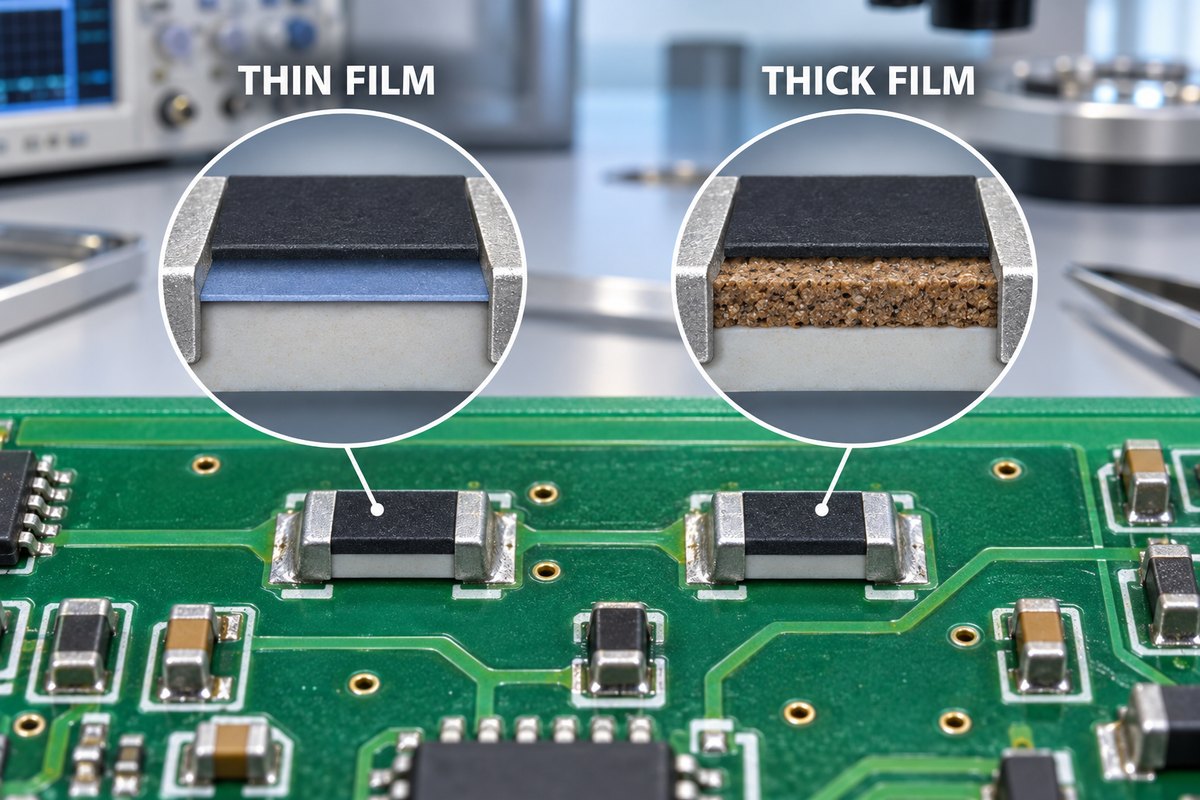
2N2222 pinout
2N2222 pinout review should connect the transistor package, footprint, BOM, and PCBA assembly direction.

What Is the 2N2222 Pinout?

The 2N2222 pinout is the pin assignment for the three terminals of a 2N2222 NPN bipolar junction transistor. The terminals are emitter, base, and collector.

The simple explanation is:

  • Emitter: current exits the transistor in typical NPN switching circuits.
  • Base: receives the control signal through a suitable resistor.
  • Collector: connects to the load side in many low-power switching designs.

That sounds simple, but it is not enough for production. The pin order depends on the exact part number, package, manufacturer datasheet, and how the transistor is viewed. A TO-92 part shown from the flat face may not match a metal-can package or an SMD package. Even similar names such as 2N2222A, PN2222A, and P2N2222A should be checked against the selected manufacturer datasheet.

For a PCB or PCBA order, the safest wording is not “2N2222 is always E-B-C.” The safer production instruction is: confirm the manufacturer part number, package, pin view, PCB footprint, and assembly orientation before release.

2N2222 Transistor Pinout and Pin Functions

A 2N2222 transistor is commonly used as a small-signal NPN transistor for switching and amplification. In many PCB products, it may drive LEDs, relays, buzzers, small motors, signal lines, or interface circuits.

Buyers usually need to confirm these pin functions before PCBA:

Pin Function What to Check in Production Files Risk if Wrong
Emitter Connected to the correct reference or return path. The transistor may not switch correctly.
Base Controlled through the correct resistor network. The transistor may stay off, overheat, or behave unstably.
Collector Matched to the load side and current path. The load may fail to operate or the part may be damaged.

For assembly teams, the pin function is only useful when it is tied to the physical footprint. A schematic may be correct, but the PCB symbol-to-footprint mapping can still be wrong. This is why transistor pinout checks should include the schematic symbol, PCB footprint pads, BOM manufacturer part number, and placement drawing.

2N2222 Pin Configuration by Package Type

The phrase “2N2222 pin configuration” often creates confusion because users may be looking at different package types. A TO-92 plastic package, TO-18 metal can, and SMD transistor package cannot be treated as one fixed layout.

Common package review points include:

  • TO-92: confirm whether the drawing is viewed from the flat face or lead side.
  • TO-18 metal can: confirm the bottom-view or top-view reference in the datasheet.
  • SOT-23 or other SMD substitutes: confirm the exact substitute part and footprint.
  • PN2222A or P2N2222A: do not assume the same pin order as another supplier’s 2N2222.

In real sourcing work, the project may start with “2N2222” in the BOM, but the available part may be a manufacturer-specific 2N2222A, PN2222A, P2N2222A, or SMD equivalent. The electrical replacement may look acceptable, but the footprint and pin order still need a separate check.

2N2222 pinout
Always confirm the exact datasheet view before releasing the transistor footprint for PCB layout or PCBA assembly.

2N2222 Pin Diagram Mistakes Before PCB Layout

A 2N2222 pin diagram can be correct on its own but still cause a wrong PCB if the view direction is misunderstood. Many drawings show the package from a specific side, and that side is easy to reverse during footprint creation.

Common mistakes before layout include:

  • Reading a bottom-view drawing as a top-view drawing.
  • Copying a generic internet pinout without checking the chosen manufacturer.
  • Using a TO-92 footprint for a different lead order.
  • Replacing a through-hole part with an SMD part without footprint review.
  • Leaving the flat-side mark unclear on the silkscreen.
  • Letting the BOM name and assembly drawing describe different packages.

For a single prototype, one wrong footprint may be repaired by cutting traces or bending leads. For a batch build, the same error can stop assembly, delay shipment, and create extra component and labor cost.

A practical DFM review should ask one direct question: if an operator looks at the PCB, BOM, and placement drawing, can they install the transistor in only one correct orientation?

2N2222A Pinout and PN2222A Pinout Differences

2N2222A and PN2222A are often discussed together because both are common NPN transistor options. However, their pinout should not be judged only by the name. The package and manufacturer matter.

For BOM substitution, check these items before approval:

  • Full manufacturer part number
  • Package code and drawing
  • Pin assignment and view direction
  • Collector current and voltage rating
  • Power dissipation and thermal condition
  • Gain range or hFE grouping
  • Lead forming or tape packaging requirement
  • Footprint compatibility with the PCB

From the buyer’s side, this is where component sourcing and assembly review should work together. A purchasing team may find an available substitute, but the engineering review must confirm whether it can be assembled on the same PCB without changing the footprint or circuit behavior.

EBest Circuit can help flag these sourcing-related manufacturing risks before production. The final electrical approval should still come from the customer’s engineering team, especially when the transistor is used near its voltage, current, gain, or thermal limits.

How to Check the 2N2222 Datasheet Before PCB Footprint Selection

The datasheet is the authority for footprint selection. Search results and quick diagrams can help explain the topic, but they should not replace the selected manufacturer’s datasheet in a production build.

A datasheet check should confirm:

  • Exact package outline
  • Lead order and view direction
  • Recommended mounting style
  • Lead diameter or pad geometry
  • Body size and height
  • Thermal limits
  • Electrical rating margin
  • Storage and soldering conditions

For through-hole designs, the footprint must match lead spacing, hole size, annular ring, soldering method, and component height. For SMD alternatives, the pad size, solder mask opening, stencil opening, and placement rotation must be reviewed.

This is also a good place to check whether the board will use FR4 PCB, high-current copper requirements, special soldering conditions, or mechanical constraints around the transistor body. The transistor may be small, but its placement can affect test access, repair access, heat concentration, and enclosure clearance.

PCB Layout Checks for a 2N2222 Transistor

PCB layout checks for a 2N2222 transistor should focus on the physical connection between schematic intent and manufacturable board data. A correct circuit on paper can still fail if the footprint, routing, or silkscreen creates assembly ambiguity.

Layout checks should include:

  • Pin mapping between schematic symbol and PCB footprint
  • Clear emitter, base, and collector pad assignment
  • Readable silkscreen orientation mark
  • Correct base resistor placement and routing
  • Load current path and copper width
  • Thermal spacing from heat-sensitive components
  • Test point access for important signals
  • Enough clearance for hand insertion or AOI review
  • No conflict between the BOM package and footprint package

For low-current signal switching, the copper requirement may be modest. For relay drive, LED arrays, motor control, or solenoid-related circuits, the current path and heat condition deserve closer attention. The PCB supplier should not redesign the circuit, but can flag layout and manufacturing issues that may affect assembly quality or repeatability.

PCBA Assembly Checks for 2N2222 Pinout and Orientation

During PCBA assembly, the 2N2222 transistor must be placed in the correct orientation and soldered with a stable process. The assembly drawing should show the package direction clearly enough that operators and inspectors do not need to guess.

Assembly checks should cover:

  • Correct transistor part number loaded for production
  • Package match between BOM and PCB footprint
  • Lead forming direction for through-hole parts
  • Placement rotation for SMD parts
  • Polarity or orientation mark on silkscreen
  • Solder joint quality after reflow, wave soldering, or hand soldering
  • AOI or visual inspection access
  • Functional test coverage after assembly

For through-hole assembly, the main concerns are lead spacing, hole fit, solder fill, component height, and post-solder inspection. For SMT assembly, the main concerns are rotation, pad size, stencil opening, component availability, and AOI recognition.

2N2222 pinout
PCBA assembly review should confirm transistor orientation, soldering quality, inspection access, and final functional test coverage.

A small transistor can be difficult to inspect after it is surrounded by taller components, connectors, heatsinks, or enclosure hardware. Good layout and assembly planning make inspection and rework easier before the board reaches the final product stage.

2N2222 Pinout Project Example for a Small Control PCB

A practical 2N2222-related PCBA project may begin with a very simple request: “Please assemble this control board.” The real manufacturing risk appears when the BOM, footprint, and component supply are checked together.

A customer developing a small industrial control PCB needed a 2N2222-family transistor to drive a buzzer and an indicator output. The first sample quantity was 50 pieces for functional validation, followed by a planned small batch after enclosure testing. The board used FR4 material, mixed SMT and through-hole parts, terminal blocks, LEDs, and several discrete components.

Project details:

  • Application: compact industrial control module
  • Quantity: 50 prototype PCBAs before small-batch production
  • Board type: FR4 PCB with mixed assembly
  • Main component concern: 2N2222-family transistor availability and orientation
  • Assembly needs: SMT placement, through-hole assembly, visual inspection, and functional test support
  • Delivery focus: quick prototype build for circuit and enclosure validation

During file review, the schematic symbol looked correct, but the BOM used a supplier-specific 2N2222A part while the footprint appeared to be copied from another TO-92 transistor. The customer also allowed substitute parts if the original part was unavailable. That created a real risk: a substitute could meet the electrical requirement but use a different pin order or package drawing.

Main checks before production:

  • Matched the BOM part number against the selected package drawing.
  • Checked emitter, base, and collector mapping against the PCB pads.
  • Flagged substitute approval as an engineering review item, not only a purchasing item.
  • Confirmed the transistor orientation mark on the assembly drawing.
  • Added functional test attention for the buzzer and indicator output.

This type of review does not change the customer’s circuit design. It protects the manufacturing result by making sure the approved design data, purchased component, PCB footprint, and assembly process all describe the same physical part.

For buyers, the value is practical: fewer assembly surprises, fewer emergency footprint corrections, and fewer delays between prototype validation and small-batch production.

FAQs About 2N2222 Pinout

Is the 2N2222 pinout always the same?
No. The pinout depends on the exact part number, package, manufacturer datasheet, and view direction. Always confirm the selected datasheet before PCB footprint release.

What are the three pins of a 2N2222 transistor?
The three terminals are emitter, base, and collector. Their physical order must be checked against the exact package drawing.

Is 2N2222A the same as PN2222A?
They are related NPN transistor options, but buyers should not assume identical package, pin order, or manufacturer specifications without datasheet review.

Can a wrong 2N2222 footprint cause PCBA failure?
Yes. A wrong footprint or reversed pin mapping can stop the transistor from switching correctly and may require rework or PCB revision.

Can EBest Circuit check 2N2222 orientation before assembly?
Yes. EBest Circuit can support PCB layout manufacturability review, BOM and footprint checks, PCBA assembly, inspection, and functional testing support based on customer-approved files.

In Conclusion, 2N2222 pinout affects more than a symbol on the schematic. It affects footprint selection, BOM substitution, silkscreen direction, soldering quality, inspection, and functional test results. Before PCB fabrication or PCBA assembly, confirm the exact datasheet, package, pin view, and assembly orientation.

EBest Circuit (Best Technology) supports PCB fabrication, PCB layout manufacturability review, component sourcing coordination, PCBA assembly, inspection, and testing support for transistor-based boards. For project review, send Gerber files, BOM, pick-and-place file, assembly drawing, and test requirements to sales@bestpcbs.com.
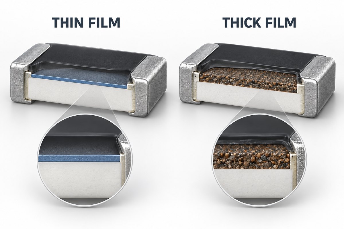
You may also like

PLCC Package: PCB Footprint, Soldering, and Assembly Guide

July 31st, 2026

A PLCC package is a plastic leaded chip carrier with J-shaped leads folded under the package body. It can be mounted in a socket or soldered directly to a printed circuit board. That flexibility made PLCC devices common in memory, controllers, processors, programmable logic, and many long-life industrial products.

For a PCB assembly buyer, however, recognizing the package name is only the beginning. The exact manufacturer part number, pin count, body dimensions, land pattern, Pin 1 orientation, component supply condition, soldering process, and inspection method must all agree. A PLCC component that looks correct can still be the wrong ordering code or a poor match for the released footprint.

This guide explains the package from a PCB and PCBA manufacturing perspective. It shows what engineers and buyers should confirm before component sourcing, stencil release, assembly, inspection, rework, and repeat production.

plcc package
PLCC package review should connect the component drawing, PCB footprint, sourcing data, and assembly plan.

What Is a PLCC Package?

PLCC means plastic leaded chip carrier. The package usually has leads on four sides, with each lead curling inward beneath the molded body in a J shape. Unlike a leadless chip carrier, a PLCC has formed metal leads. Unlike a typical QFP, its leads do not extend outward as long gull-wing terminals.

Many PLCC families use a 1.27 mm lead pitch, but the package name alone does not establish the complete mechanical specification. Different devices can have different pin counts, body sizes, heights, tolerances, ordering codes, moisture-handling requirements, and manufacturer-recommended footprints. The current component datasheet and package drawing must control the build.

PLCC devices may be directly soldered to the PCB or installed in a matching socket. A socket makes component removal or replacement easier, but it also adds height, cost, contacts, and another mechanical interface. Direct soldering creates a lower-profile assembly but makes replacement more dependent on controlled rework.

If an incoming part must be identified from its body markings, use the marking, BOM, manufacturer documentation, package dimensions, and board records together. The PCB components identification guide explains why one visible code is not enough to approve a component for production.

How Does a PLCC Package Connect to a PCB?

A directly soldered PLCC sits over perimeter pads on the PCB. Solder paste is printed on the lands, the component is placed with the correct orientation, and the assembly passes through the approved reflow process. The solder joints form around the exposed lower portions of the J-leads.

The inward lead shape saves board area, but it also changes what can be seen after soldering. Part of each termination is close to or under the package body. This means a board can look generally acceptable from above while still requiring closer inspection of lead wetting, alignment, bridging, insufficient solder, or lifted leads.

A socketed build follows a different path. The PCB is assembled with the PLCC socket, and the IC is inserted later. The socket footprint, socket orientation, insertion method, retention, overall height, and access for removal all become part of the assembly review.

Before choosing the mounting method, confirm:

  • whether the released BOM calls for the IC alone or an IC-and-socket combination;
  • whether field replacement or programming access requires a removable device;
  • whether the enclosure allows the added socket height;
  • whether vibration, contact resistance, thermal cycling, or handling affects the product requirement;
  • whether the production quantity and test flow support manual insertion after reflow.

The customer’s product team remains responsible for the electrical and system-level choice. EBest Circuit (Best Technology) can review the released PCB, BOM, CPL, assembly drawing, and process notes for manufacturing conflicts before PCBA production.

PLCC Package Sizes, Pin Counts, and Footprints

PLCC is a package family, not one universal outline. Common devices include square and rectangular bodies with different pin counts. Manufacturer drawings also define body dimensions, lead pitch, lead width, seating details, tolerances, and the Pin 1 index area.

The risk appears when a BOM uses only a generic description such as “PLCC-44” while the PCB library was created from a different device or socket drawing. The pin count may match, but the body, lead geometry, courtyard, socket requirements, or recommended land pattern may not.

Use this identification chain before approving the footprint:

  • complete manufacturer part number and ordering code;
  • manufacturer and current datasheet revision;
  • package name, pin count, pitch, and drawing code;
  • body width, body length, and maximum seated height;
  • terminal dimensions and recommended PCB land pattern;
  • Pin 1 marking and pin-numbering direction;
  • tube, tray, tape, or other delivery format needed for assembly.

For example, Microchip publishes separate PLCC package outline drawings, while NXP lists package-specific dimensions and mounting details for PLCC families. These sources illustrate why a generic package label should never replace the exact component drawing.

The existing guide to part number width specifications provides a broader method for reconciling ordering codes, package drawings, tolerances, land patterns, and incoming parts.

Socketed vs Soldered PLCC Assembly

Decision Socketed PLCC Directly soldered PLCC
Replacement Easier device removal Requires controlled rework
Assembly height Higher Lower
Interfaces Socket plus IC contacts Solder joints to PCB
Production steps Socket assembly and IC insertion Placement and reflow

A socket is useful when the component must be removed for programming, service, configuration, or replacement. It can also protect the IC from the primary soldering process when the released product plan requires later insertion.

But a socket is not automatically the safer manufacturing option. A mismatched socket, reversed socket, bent contact, incomplete insertion, or excessive insertion force can stop the board at test. Added height may also interfere with an enclosure or neighboring hardware.

Direct soldering eliminates the socket interface and supports automated SMT assembly. The process must still match the component’s approved storage, handling, placement, and reflow requirements. Old or separately sourced PLCC stock should not be released to the line only because the part number appears correct.

For repeat builds, record the approved part, socket if used, footprint revision, orientation image, insertion step, inspection criteria, and any programming sequence. These records reduce the risk of the next lot being built from an incomplete purchasing description.

How Should a PLCC Footprint Be Reviewed?

A footprint review does not redesign the circuit. It compares the released component data with the PCB land pattern and the needs of fabrication, assembly, inspection, and rework.

Key review points include:

  • Land geometry. Compare pad length, width, pitch, and location with the current manufacturer recommendation or the customer-approved library standard.
  • Pin 1 control. The PCB, silkscreen, assembly drawing, CPL rotation, and component marking must communicate the same orientation.
  • Solder mask and paste. Openings must support the released pad and stencil strategy without creating avoidable bridging or insufficient solder risk.
  • Courtyard and access. Nearby components, sockets, connectors, enclosure parts, and rework tools need adequate clearance.
  • Board support. Large packages and sockets should not sit in areas where panel handling, depaneling, or board flex creates unnecessary mechanical stress.
  • Inspection visibility. The layout should allow the planned inspection method to view the relevant lead areas.

A common failure scenario is a correct IC placed on a footprint copied from an unrelated PLCC library entry. The board reaches SMT, but the land geometry or orientation convention does not match the released part. Production then stops for engineering clarification, stencil revision, PCB rework, or a new board revision.

Sending the exact package drawing with the Gerber or ODB++, BOM, CPL, and assembly drawing lets the PCBA supplier raise this conflict before materials and schedules are committed.

plcc package
Footprint and Pin 1 alignment should be confirmed before the PLCC component is released for placement.

Common PLCC Soldering and Assembly Problems

PLCC assembly problems are usually not caused by the package name itself. They come from mismatched data, uncontrolled materials, or a process that does not account for the J-lead geometry.

Wrong orientation. If the CPL rotation, silkscreen mark, drawing, and package index are inconsistent, a correctly sourced component can be placed 90 or 180 degrees from the intended orientation. Clear Pin 1 documentation and first-article confirmation reduce this risk.

Solder bridging. Excess paste, poor alignment, inappropriate stencil openings, contamination, or lead damage can connect adjacent terminations. The consequence may be an immediate electrical short or a board that fails powered testing.

Insufficient solder or poor wetting. Storage condition, surface contamination, lead finish, paste transfer, land geometry, or reflow conditions can leave a weak or incomplete joint. A simple top view may not show the full condition around the J-lead.

Lifted or damaged leads. Improper handling, unsuitable packaging, or uncontrolled rework can deform a lead. The component may still sit on the board while one termination does not contact the land correctly.

Package-to-footprint mismatch. A buyer approves an alternate with the same function and pin count, but the package drawing is different. This can cause placement, soldering, clearance, or inspection problems even before electrical compatibility is considered.

Uncontrolled legacy stock. A part may be obsolete, aged, repacked, or supplied without enough traceability and handling information. The sourcing decision should be completed before the SMT schedule is fixed. See the BestPCBS component sourcing resources for the BOM information buyers should prepare.

How Are PLCC Solder Joints Inspected?

Inspection should answer a defined risk question. It should not be added as a generic line in the quotation without clear coverage.

Visual inspection can check orientation, body damage, obvious offset, exposed lead condition, and visible solder quality. AOI can support repeatable checks for placement, polarity, bridging, and other visible conditions when the package and board geometry provide a usable camera view.

However, AOI cannot prove component function, and the inward J-lead shape limits visibility compared with a long outward gull-wing lead. If the acceptance requirement depends on an area that is not adequately visible, the customer and supplier should agree on another suitable method rather than claiming that AOI proves every joint.

Electrical or functional testing addresses a different question: whether the assembled board behaves according to the customer’s defined test plan. Testing requires suitable test points, firmware or programming files when applicable, fixtures or connection instructions, limits, and pass/fail criteria.

The AOI in PCB manufacturing guide explains how AOI differs from SPI, X-ray, electrical checks, and functional testing.

plcc package
PLCC inspection should combine visible workmanship checks with the electrical or functional test coverage defined by the customer.

PLCC vs QFP and BGA Packages

Package Connection style Manufacturing consideration
PLCC J-leads under body edge Socket option and partial joint visibility
QFP Gull-wing leads extend outward Lead coplanarity and fine-pitch handling
BGA Solder balls under package Hidden joints and X-ray planning

PLCC, QFP, and BGA describe different mechanical connection systems. They should not be treated as interchangeable simply because two devices offer similar electronic functions.

A QFP usually provides more visible solder joints, but its outward leads increase the package footprint and can be vulnerable to handling damage. A BGA supports a high connection count beneath the body, but its joints are hidden and require a different land pattern, stencil strategy, reflow process, and inspection plan.

The package choice belongs to the customer’s electronic and product design team. From the manufacturing side, the important task is to build the released package correctly and identify when the BOM, footprint, placement data, inspection access, and replacement plan do not agree.

What Should You Send for a PLCC PCBA Quote?

A quotation based only on board size, layer count, and the phrase “PLCC assembly” leaves too many assumptions open. A useful RFQ connects the component, PCB, assembly process, inspection, testing, and delivery requirement.

Send these files and decisions:

  • Gerber or ODB++ files, NC drill data, and fabrication drawing;
  • complete BOM with exact manufacturer part numbers and approved alternates;
  • CPL or centroid file with designators, coordinates, side, and rotation;
  • assembly drawing with Pin 1, polarity, no-fit, and special handling notes;
  • PLCC manufacturer datasheet and package drawing;
  • socket manufacturer part number and insertion instructions, if applicable;
  • customer-supplied versus supplier-sourced component responsibility;
  • inspection, programming, functional test, acceptance, and packing requirements;
  • prototype and production quantities plus the requested delivery schedule.

A realistic production example. A buyer requests 100 controller PCBAs using a legacy 44-lead PLCC. The BOM lists a shortened part number, while the PCB library name only says “PLCC44.” One supplier quotes immediately. Another supplier asks for the complete ordering code and package drawing, then finds that the proposed substitute and the released land pattern do not share the same approved mechanical details.

The second supplier has not redesigned the product. It has prevented an unapproved assumption from reaching purchasing and SMT. The buyer can now confirm the exact component, approve a documented alternate, or revise the released footprint before ordering boards and material.

When delivery is urgent, the same principle applies. The fast PCB assembly guide explains why BOM and DFM review should happen before an accelerated schedule is promised.

EBest Circuit (Best Technology) can support PCB manufacturability review, PCB fabrication, BOM sourcing, SMT and mixed PCBA, inspection, and testing assistance based on customer-provided specifications. Send the files above to sales@bestpcbs.com for a quotation review.

FAQs About PLCC Packages

What does PLCC mean?

PLCC means plastic leaded chip carrier. It is an IC package family commonly identified by J-shaped leads along the package sides.

Can a PLCC package be soldered directly to a PCB?

Yes. Many PLCC devices can be directly soldered to an approved PCB land pattern. The exact component datasheet, footprint, handling, and assembly requirements must be followed.

Can every PLCC device use a socket?

No. The device pin count, outline, socket specification, orientation, height, and product requirements must match. A generic PLCC description does not prove socket compatibility.

Is a PLCC footprint determined only by pin count?

No. Pin count is only one identifier. Confirm the complete ordering code, pitch, body dimensions, terminal geometry, package drawing, recommended land pattern, and Pin 1 convention.

Can EBest Circuit help assemble boards with PLCC components?

Yes, when the released PCB and assembly package is complete. EBest Circuit can support manufacturability review, PCB fabrication, BOM sourcing, PCBA, inspection, and agreed testing assistance. The customer remains responsible for component selection and electrical design approval.

If your next PLCC package project needs PCB fabrication, component sourcing, assembly review, inspection planning, or a build quotation, send your Gerber or ODB++ files, BOM, CPL, package drawing, quantities, and test requirements to sales@bestpcbs.com.
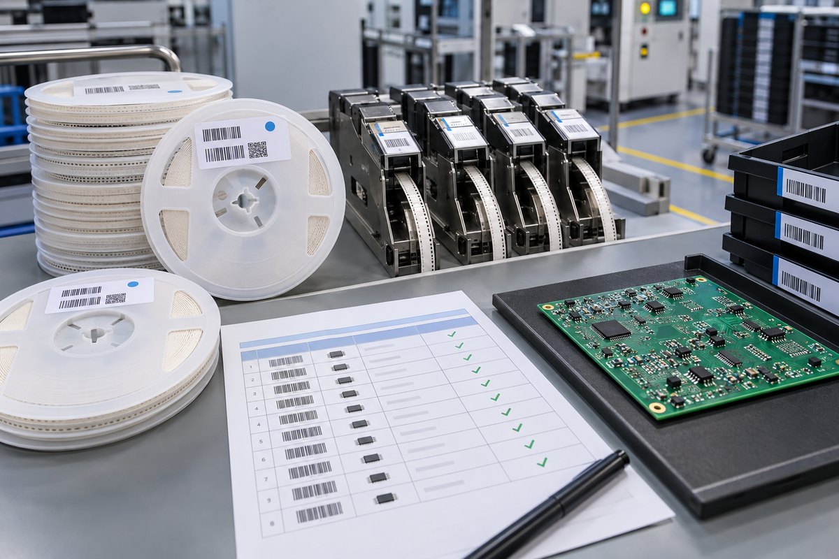
You may also like

PCB Transformer Guide for Layout and PCBA Assembly

July 31st, 2026

A pcb transformer can mean different things in electronics manufacturing. In most PCB and PCBA projects, it refers to a transformer mounted on a printed circuit board, or a transformer structure that is integrated into the board design for voltage conversion, isolation, signal coupling, or power regulation.

For engineers and buyers, the real question is not only “what transformer should I use?” The bigger production question is whether the PCB layout, copper design, clearance, creepage, soldering process, mechanical support, BOM, and inspection plan can support the transformer safely and repeatably.

pcb transformer
PCB transformer projects should be reviewed as complete PCB and PCBA builds, not only as transformer component choices.

EBest Circuit (Best Technology) supports PCB fabrication, BOM review, component sourcing, SMT assembly, through-hole assembly, mixed PCBA production, inspection, and testing coordination for transformer-related PCB and PCBA projects. If your project includes PCB-mounted transformers, planar transformers, isolation transformers, or power transformer circuits, our team can review the manufacturing files and assembly requirements before production.

What Is a PCB Transformer?

A PCB transformer is usually a transformer used on a printed circuit board. It may be a discrete PCB mount transformer soldered onto the board, or a transformer structure created with copper windings, magnetic cores, and insulation features in the PCB design.

In this article, PCB means printed circuit board. It does not refer to PCB chemicals in transformer oil, disposal, contamination, or environmental regulations.

In electronics, a PCB transformer is commonly used for:

  • Voltage step-down or step-up
  • Electrical isolation between input and output circuits
  • Signal coupling
  • Noise reduction
  • Impedance matching
  • Power conversion in compact products
  • Safety separation in control and power boards

A PCB transformer can appear in power adapters, industrial controllers, LED drivers, communication equipment, medical electronics, automotive modules, energy storage devices, and other products where controlled power transfer or isolation is required.

For production teams, the transformer is not only a component on the BOM. It affects the board layout, copper thickness, thermal behavior, assembly method, solder joint strength, inspection plan, and final test requirements.

PCB Mount Transformer vs Transformer Built Into a PCB

A PCB mount transformer and a transformer built into a PCB are related, but they are not the same manufacturing situation.

Type What It Means Main Manufacturing Focus
PCB mount transformer A finished transformer component soldered onto the PCB Footprint, pin fit, soldering, height, clearance, mechanical support
Through-hole transformer A larger transformer with pins inserted through plated holes Hole size, annular ring, solder fill, board support, wave or hand soldering
SMT transformer A surface-mount transformer placed by SMT process Pad design, solder paste, reflow profile, coplanarity, AOI limits
Planar transformer PCB Windings are formed by PCB copper layers Stackup, copper thickness, insulation, alignment, thermal path
Transformer circuit board A board that carries transformer-related power or isolation circuits Creepage, clearance, copper width, slots, testing, safety documentation

A PCB mount transformer is usually easier for buyers to source because it is a standard component. The customer provides the transformer part number, datasheet, BOM, Gerber files, and assembly drawing. The PCBA supplier then checks whether the footprint, soldering process, and board design are manufacturable.

A planar transformer PCB is more demanding. The PCB itself becomes part of the magnetic structure, so copper thickness, layer registration, dielectric thickness, insulation spacing, and process tolerance become more critical.

For EBest Circuit, the correct role is manufacturing and assembly support. We can review whether the PCB and PCBA files are suitable for production, but the customer’s engineering team should define the transformer electrical design, safety standard, magnetic design, and approved component specification.

How Does a Transformer on Circuit Board Work?

A transformer on circuit board works by electromagnetic induction. The primary side receives an AC or switching signal. The changing current creates magnetic flux, and the secondary side receives induced voltage through magnetic coupling.

In practical PCB projects, the transformer may work in different ways depending on the circuit:

  • In an AC-DC power board, it may step down voltage and provide isolation.
  • In a flyback converter, it may store and transfer energy between switching cycles.
  • In a signal isolation circuit, it may transfer signals while separating grounds.
  • In a communication circuit, it may support impedance matching and noise control.
  • In a current sensing design, it may help measure current without direct electrical connection.

The PCB layout around the transformer matters because high voltage, high current, switching noise, and heat can all concentrate in the same area.

Key production-related risks include:

  • Primary and secondary spacing is too small.
  • Copper width is not enough for current.
  • Thermal relief affects soldering or heat flow.
  • Transformer body blocks nearby inspection points.
  • Tall components interfere with enclosure clearance.
  • Pin pitch does not match the actual transformer datasheet.
  • Silkscreen or polarity marks are unclear.
  • Slots, cutouts, or keepout zones are missing.

A transformer can be electrically correct in the schematic but difficult to build if the PCB and assembly details are not controlled early.

PCB Transformer Board Requirements Before Production

Before a PCB transformer board enters production, the PCB supplier should not only look at board size, layers, and quantity. The board needs a manufacturing review around power, isolation, heat, and assembly risk.

Key files to prepare before quotation:

  • Gerber files
  • NC drill file
  • PCB stackup
  • Finished copper thickness
  • Board thickness
  • Surface finish
  • BOM
  • Pick-and-place file
  • Assembly drawing
  • Transformer datasheet
  • Safety or creepage requirements if applicable
  • Test procedure if PCBA testing is required

For transformer-related PCB boards, several areas deserve special attention.

Clearance and creepage

Clearance is the direct air distance between conductive parts. Creepage is the distance along the board surface. Transformer circuits may require larger spacing between primary and secondary sides, especially when the board handles AC input, high voltage, or safety isolation.

If the design needs slots, isolation grooves, wider spacing, or special coating, these requirements should be shown clearly in the fabrication notes.

Copper width and copper weight

Transformer circuits often carry higher current than small signal circuits. Copper width, copper thickness, via count, and thermal path should match the current and heat requirement. If copper is too narrow, the board may pass initial testing but run hot during long operation.

Hole and pad reliability

For through-hole transformers, plated through holes need proper hole size, annular ring, solderability, and mechanical strength. Large transformer pins, thick leads, or heavy bodies can create stress during insertion, soldering, transportation, or product use.

Board material and thickness

Most transformer carrier boards use FR4, but high-temperature, high-current, or compact power designs may need higher Tg material, heavier copper, or special stackup review. For planar transformer PCBs, dielectric thickness and copper layer structure become part of the design result.

Marking and orientation

Transformer direction, pin 1, primary side, secondary side, and polarity marks should be visible on the silkscreen or assembly drawing. Ambiguous marking can cause assembly mistakes, especially in mixed SMT and through-hole production.

How to Control PCB Transformer Assembly and Inspection Quality?

PCB transformer assembly quality depends on the transformer package, weight, pin type, soldering method, and how the board will be used after shipment.

pcb transformer
PCB transformer assembly quality depends on footprint fit, soldering process, inspection access, and functional test planning.

For SMT transformers, the main risks are solder paste volume, pad design, component shift, reflow profile, and hidden solder joint defects. For through-hole transformers, the main risks are hole fit, solder fill, pin wetting, flux residue, and mechanical stress.

Important assembly checks include:

  • Confirm transformer part number against BOM and datasheet.
  • Check package size, pin pitch, and mounting direction.
  • Verify polarity and primary/secondary orientation.
  • Review solder paste opening for SMT transformer pads.
  • Confirm through-hole pin insertion and solder fill.
  • Inspect heavy transformer body support.
  • Check clearance around heat-sensitive plastic parts.
  • Review wave soldering or selective soldering feasibility.
  • Confirm AOI visibility and manual inspection points.
  • Add functional testing when the customer provides test procedures.

A transformer may be too tall or too heavy for a weak board support area. If the product will face vibration, transportation shock, or repeated plug-in force nearby, mechanical review is important. In some projects, adhesive, extra fixture support, conformal coating, or mechanical fasteners may be needed, depending on customer drawings and product requirements.

For PCBA inspection, AOI is helpful but not enough for every transformer assembly. Large bodies can block solder joints. Through-hole solder joints may require visual inspection from both sides. Functional testing is often more useful when the board includes voltage conversion, isolation, or power output requirements.

EBest Circuit can support inspection planning based on customer files, including AOI, visual inspection, X-ray when applicable, and functional testing coordination when test instructions and fixtures are provided.

Planar Transformer PCB Requirements for High-Frequency Power Boards

A planar transformer PCB is different from a normal board carrying a transformer component. In a planar transformer design, the PCB copper layers form transformer windings. This makes PCB fabrication quality directly affect electrical behavior.

pcb transformer
Planar transformer PCB fabrication requires controlled copper geometry, dielectric spacing, and clear manufacturing notes.

Planar transformer PCB projects are commonly used in high-frequency power supplies, compact DC-DC converters, telecom power modules, EV-related electronics, industrial power boards, and other products where space, efficiency, and repeatability matter.

Planar transformer PCB requirements often include:

  • Controlled PCB stackup
  • Stable dielectric thickness
  • Accurate layer registration
  • Suitable copper thickness
  • Clear winding geometry
  • Reliable via structure
  • Consistent insulation spacing
  • Good thermal path
  • Clean routing between primary and secondary areas
  • Clear fabrication notes

The manufacturing risk is higher because small changes in copper geometry, dielectric spacing, or layer alignment can affect performance. The PCB supplier should review whether line width, spacing, copper thickness, drilling, lamination, plating, and routing requirements match the actual manufacturing capability.

For buyers, the RFQ should not only say “planar transformer PCB.” It should include stackup, copper weight, material, insulation requirement if needed, working voltage, board thickness, surface finish, and any special acceptance criteria.

EBest Circuit can review planar transformer PCB fabrication files from a manufacturability perspective and advise whether the structure fits available PCB process capability.

Power Transformer PCB Risks Buyers Should Confirm Before RFQ

A power transformer PCB is often part of a product where heat, current, safety, and reliability are more important than simple board cost.

Buyers should confirm several practical risks before sending an RFQ.

Project requirements:

  • Input and output voltage range
  • Current and power rating
  • Transformer part number or approved alternatives
  • PCB copper thickness
  • Minimum clearance and creepage
  • Board material and Tg requirement
  • Thermal management requirement
  • Assembly method
  • Inspection standard
  • Functional test requirement
  • Coating or potting requirement
  • Delivery schedule and quantity

Common quotation problems:

  • Transformer datasheet is missing.
  • BOM part number does not match the footprint.
  • Gerber files do not show enough isolation spacing.
  • Copper thickness is not specified.
  • Assembly drawing does not show transformer direction.
  • High-current nets are not clearly marked.
  • Testing requirement is discussed only after assembly.
  • Coating or potting is requested after quotation.
  • Packaging requirements are not defined for tall components.

For production, these details affect cost and lead time. A board with a large through-hole transformer may need different soldering control than a compact SMT board. A power board with high current may need thicker copper or wider traces. A board with safety isolation may need larger spacing, slots, or clearer documentation.

A good supplier should help identify these manufacturing risks before production, not after the first batch fails inspection.

How EBest Circuit Supports PCB Transformer Projects

EBest Circuit (Best Technology) supports PCB transformer projects from PCB fabrication to PCBA assembly when customers provide the approved design files, BOM, transformer specifications, and production requirements.

EBest Circuit supports transformer-related PCB and PCBA projects with:

  • PCB fabrication for FR4, multilayer, heavy copper, high Tg, and special PCB requirements
  • DFM review for manufacturability before production
  • BOM review and component sourcing support
  • SMT assembly for surface-mount transformer and related components
  • Through-hole assembly for larger PCB mount transformers
  • Mixed assembly for power boards with SMT and THT components
  • AOI and visual inspection
  • X-ray inspection when applicable
  • Functional testing coordination based on customer test instructions
  • Prototype, small-batch, and production support

For transformer-related boards, our engineering review can help check whether the PCB layout, hole size, copper thickness, soldering process, component spacing, and assembly notes are clear enough for production.

EBest Circuit does not replace the customer’s electrical design team. The customer should define the transformer electrical specification, magnetic design, safety standard, and final performance targets. Our value is helping turn approved design files into reliable PCB and PCBA production with practical manufacturing control.

If your PCB or PCBA project includes PCB-mounted transformers, planar transformer structures, high-current power sections, or isolation circuits, send your files to sales@bestpcbs.com for engineering review and quotation.

PCB Transformer Case Example for a Power Control Board

A European industrial equipment customer prepared a small-batch power control board for a 24 V control system. The board included a through-hole PCB mount transformer, relays, terminal blocks, fuses, electrolytic capacitors, and mixed SMT control components.

Project requirements:

  • Country: Germany
  • Quantity: 120 pcs pilot run
  • Application: industrial control power module
  • Board type: FR4 multilayer PCB with mixed SMT and through-hole assembly
  • Key component: through-hole PCB mount transformer
  • Delivery requirement: pilot batch for functional validation

The first concern was not whether the transformer could be purchased. The real production issue was whether the board could be assembled and inspected reliably.

Main challenges:

  • The transformer body was tall and heavier than surrounding components.
  • Primary and secondary areas needed clear separation.
  • The transformer pins required stable solder fill.
  • The BOM had one alternate transformer with slightly different pin dimensions.
  • The assembly drawing did not clearly mark the transformer orientation.
  • The customer needed functional testing after assembly.

During DFM and assembly review, EBest Circuit checked the transformer footprint, pin hole size, soldering method, component keepout area, and inspection accessibility. The BOM was reviewed against the transformer datasheet, and the alternate part was flagged for confirmation before sourcing.

EBest Circuit solution:

  • Confirmed transformer footprint and pin spacing before production
  • Reviewed hole size and annular ring for through-hole soldering
  • Checked spacing around transformer primary and secondary areas
  • Recommended clearer assembly marking for transformer orientation
  • Coordinated SMT and through-hole assembly sequence
  • Added manual inspection for transformer solder joints
  • Followed customer-provided functional test steps after assembly
  • Packed the boards with protection for tall components

This type of project shows why a PCB transformer board should not be treated like a simple bare PCB order. The transformer affects fabrication, assembly, inspection, testing, and packaging. When those details are reviewed before production, buyers have fewer surprises during pilot build and batch delivery.

FAQs About PCB Transformer

What is a PCB transformer?

A PCB transformer is a transformer used on or built into a printed circuit board. It may be a PCB mount transformer component or a transformer structure created with PCB copper windings and magnetic core materials.

Is a PCB transformer the same as PCB transformer oil?

No. In electronics manufacturing, PCB means printed circuit board. PCB transformer oil usually refers to polychlorinated biphenyl contamination or environmental disposal topics, which are not the same as PCB and PCBA manufacturing.

Can EBest Circuit manufacture transformer components?

EBest Circuit supports PCB fabrication, component sourcing, PCBA assembly, inspection, and testing coordination. We do not claim to design or manufacture transformer magnetic components themselves. Customers should provide approved transformer part numbers, datasheets, and design requirements.

What files are needed for a PCB transformer PCBA quote?

Please provide Gerber files, NC drill files, BOM, pick-and-place file, assembly drawing, transformer datasheet, quantity, surface finish, copper thickness, testing requirements, and delivery target.

Why is clearance and creepage important on a PCB transformer board?

Transformer circuits may separate high-voltage and low-voltage areas. Proper clearance and creepage help reduce arcing, leakage, and insulation risk. The required spacing depends on the product standard, voltage, environment, and design requirement.

In Conclusion, a pcb transformer project should be reviewed as a complete PCB and PCBA manufacturing task, not only as a transformer component selection issue. The transformer affects layout spacing, copper design, thermal behavior, soldering, inspection, testing, and packaging.

EBest Circuit (Best Technology) supports PCB fabrication, DFM review, component sourcing, PCBA assembly, inspection, and testing coordination for transformer-related PCB projects. To review your Gerber files, BOM, transformer datasheet, assembly drawing, and production requirements, contact sales@bestpcbs.com.
You may also like

Practical HDMI RF Modulator Component Guide for PCBA Projects

July 30th, 2026

HDMI RF modulator component projects are used when HDMI video and audio need to be converted into an RF signal that can travel through coaxial cable to TVs, distribution systems, test equipment, or RF-based video networks. For buyers, the search is often about finding the right product or module. For engineers, the more practical question is whether the HDMI input, RF output, power circuit, shielding, connectors, and assembly process can work together reliably on a real PCB or PCBA.

EBest Circuit (Best Technology) supports PCB fabrication, component sourcing, SMT assembly, through-hole assembly, DFM review, inspection, testing coordination, and small-batch PCBA production for RF-related electronic products. If your HDMI RF modulator project already has Gerber files, BOM, CPL, stackup notes, connector drawings, or testing requirements, you can send them to sales@bestpcbs.com for an engineering review before production.

hdmi rf modulator component
HDMI RF modulator component PCB and RF output testing scene.

What Is an HDMI RF Modulator Component?

An HDMI RF modulator component is part of a circuit or module that helps convert an HDMI input signal into an RF output signal. In finished products, this function may appear inside an HDMI RF modulator box, an HDMI-to-coax converter, a video distribution device, or a custom RF video board.

In simple terms, the signal path usually starts from an HDMI input and ends at an RF output connector. Between these two points, the board may include video processing, modulation, clock control, power regulation, RF filtering, amplification, shielding, and output matching.

A typical HDMI RF modulator-related board may include:

  • HDMI input connector
  • ESD protection components
  • HDMI receiver or video processing IC
  • RF modulator IC or module
  • Crystal or oscillator
  • Power management circuit
  • RF amplifier stage
  • Filter network
  • Shielding structure
  • Coaxial, F-type, or SMA connector
  • Test points and programming interface

For PCB and PCBA work, the component itself is only one part of the project. The surrounding layout, stackup, grounding, impedance, connector mounting, soldering quality, and final testing often decide whether the assembled board works reliably.

How Does an HDMI to RF Modulator Component Work?

An HDMI to RF modulator component helps change a digital HDMI signal into an RF signal that can be distributed through coaxial cable.

hdmi rf modulator component
Simplified HDMI input to RF output signal path.
Stage Main Function
HDMI input Receives video and audio
Processing IC Handles signal conversion
Modulator Creates RF output format
RF stage Filters or amplifies signal
Output connector Sends signal to coax system

In a commercial HDMI RF modulator product, the circuit may support different output standards, channel settings, resolutions, or control functions. Those functions depend on the customer’s electronic design and selected chipset.

For EBest Circuit, the role is not to redefine the HDMI or RF design. The customer’s engineering team should define the circuit function, IC selection, modulation requirement, firmware, and RF performance target. Our role is to help confirm whether the approved PCB files, BOM, materials, assembly notes, and testing requirements can move into manufacturing with fewer avoidable risks.

This distinction matters. A circuit may be correct in theory, but problems can still appear during PCB fabrication or PCBA assembly if the connector footprint, RF trace, shielding pad, solder mask opening, grounding, or component package is not handled correctly.

Main Components Inside an HDMI RF Modulator Board

An HDMI RF modulator board usually combines digital video circuitry and RF circuitry on one assembly. That makes the manufacturing review more sensitive than a simple low-speed control board.

Key component groups usually include:

  • HDMI interface parts: HDMI connector, ESD diodes, common-mode filters, input protection.
  • Processing and modulation parts: HDMI receiver, video processing IC, RF modulator IC, memory, clock source.
  • RF output parts: RF amplifier, filter, matching network, coax connector, SMA connector, or F-type connector.
  • Power parts: DC input connector, regulators, inductors, capacitors, ferrite beads, power filtering.
  • Mechanical and shielding parts: shielding cans, connector shells, screws, mounting holes, enclosure contacts.
  • Testing and control parts: test pads, programming pads, switches, LEDs, headers, communication interface.

The BOM should make critical choices clear:

  • Exact HDMI connector model
  • RF connector type and drawing
  • IC package and footprint
  • Substitute rules for RF components
  • Impedance or RF path notes
  • Shielding parts and soldering method
  • Inspection and test requirements

If an HDMI connector or RF connector is changed during sourcing, the PCB footprint and assembly method may also need to be reviewed. A similar connector is not always a safe substitute.

RF HDMI Modulator Component PCB Layout and Signal Path

An RF HDMI modulator component project usually has two different signal worlds on the same PCB: high-speed digital HDMI signals and RF output signals.

The HDMI side may need controlled routing, ESD protection, short signal paths, and stable reference planes. The RF side may need 50 ohm routing, clean grounding, short matching paths, shielding, and a stable connector transition.

For manufacturing review, several areas deserve attention:

  • HDMI connector footprint and soldering strength
  • ESD component placement near the input
  • RF output connector footprint
  • Ground pad and via stitching around RF path
  • Solder mask opening near RF pads
  • Shielding can pad design
  • Distance between noisy power circuits and RF path
  • Board edge tolerance for edge or coax connectors
  • Test point access after assembly

The PCB manufacturer should not change the customer’s RF layout without approval. However, the manufacturer should check whether the design files are clear enough for production.

For example, if the RF connector drawing requires a specific board thickness, plating area, solder mask clearance, or mechanical keepout, those details should be visible before fabrication starts. If the shielding can needs solderable pads, those pads must match the real component and assembly process.

50 Ohm Routing for HDMI RF Modulator Component Boards

Many HDMI RF modulator component boards require 50 ohm control on the RF output path. The actual requirement should come from the customer’s RF design file, impedance note, or connector/module datasheet.

Factor Why It Matters
Trace width Affects impedance
Dielectric thickness Changes RF field geometry
Copper thickness Affects finished trace
Reference plane Provides return path
Solder mask May affect RF trace slightly
Connector launch Affects transition quality
Ground vias Help stabilize RF return

For lower-frequency or less sensitive products, carefully controlled FR4 may be acceptable. For higher-frequency, low-loss, or more demanding RF products, the material may need closer review. Some projects may require RF laminate, high-Tg FR4, hybrid stackup, or tighter impedance confirmation.

EBest Circuit can review stackup, copper thickness, material, impedance notes, and RF connector area before production. If the customer requires an impedance coupon or impedance test report, that should be planned before fabrication, not added after the board is already made.

4K HDMI to RF Modulator Component Manufacturing Checks

A 4K HDMI to RF modulator component board usually has tighter expectations than a basic video converter. Even when the PCB manufacturer is not responsible for the video algorithm or product design, the board still needs stable fabrication and assembly control.

For a 4K modulator related project, customers may care about signal stability, heat control, HDMI connector reliability, RF output consistency, shielding effectiveness, power noise reduction, firmware access, production repeatability, and final functional test method.

Important manufacturing questions include:

  • Is the HDMI connector footprint correct?
  • Are fine-pitch ICs suitable for the SMT process?
  • Are QFN, BGA, or exposed-pad components handled correctly?
  • Is the RF output path protected from unnecessary process variation?
  • Is the board thickness suitable for connectors and enclosure?
  • Are shielding cans, thermal pads, and test points accessible?
  • Are programming and functional testing steps defined before shipment?

A 4K product can fail for many reasons, including firmware, chipset selection, signal standard, or system-level compatibility. PCB and PCBA problems should not be added to that risk. Clean files, controlled fabrication, accurate SMT, and practical testing help make the first build easier to evaluate.

8 Channel HDMI RF Modulator Component PCB and PCBA Needs

An 8 channel HDMI RF modulator component project may involve more connectors, more heat, more RF paths, and more assembly risk than a single-channel board.

Compared with a one-channel design, an 8-channel board may need stronger attention to:

  • Connector spacing
  • Channel-to-channel isolation
  • Shielding arrangement
  • Power distribution
  • Thermal spreading
  • RF output routing
  • Enclosure alignment
  • Test coverage
  • Labeling and packing

The board may include multiple HDMI inputs, multiple processing sections, RF output circuits, and control interfaces. Even if the circuit is modular, the PCBA still needs stable production handling.

For this type of project, panelization and inspection planning become important. A larger or denser board should be reviewed for warpage, connector stress, SMT support, and test access. If the product uses many HDMI connectors or coax connectors, mechanical strength and solder joint reliability should be checked carefully.

For small-batch production, customers often need more than bare PCB fabrication. They may need component sourcing, SMT assembly, manual soldering, connector assembly, testing, packing, and documentation under one workflow. That is where a one-stop PCB and PCBA supplier can reduce communication gaps.

BOM Sourcing and SMT Assembly for HDMI RF Modulator Components

BOM sourcing is often one of the biggest risks in HDMI RF modulator component projects. Some parts may have similar names but different packages, footprints, frequency ranges, temperature ratings, or mounting requirements.

hdmi rf modulator component
PCBA inspection and RF output testing for an HDMI RF modulator board.

Before SMT, the BOM should confirm:

  • Exact HDMI connector model
  • Exact RF connector model
  • Modulator IC or module part number
  • Crystal or oscillator specification
  • Regulator current rating
  • RF filter and matching parts
  • Shielding can model
  • Package size for all fine-pitch parts
  • Approved alternate components
  • Customer-supplied or supplier-sourced parts
  • Testing and programming notes

SMT assembly also needs practical attention. HDMI connectors, QFN packages, RF shields, exposed-pad ICs, small passives, and coax connectors may require different process controls.

Typical PCBA checks include:

  • Solder paste printing
  • SPI
  • Pick-and-place accuracy
  • Reflow profile
  • AOI inspection
  • X-Ray when needed
  • Manual soldering for selected connectors
  • Cleaning requirements
  • Functional test coordination
  • Final packing protection

EBest Circuit supports both PCB fabrication and PCBA assembly, so the same project notes can stay visible from file review to shipment. This is useful when a board includes mixed requirements such as HDMI interface, RF path, shielding, SMT, through-hole connectors, and functional testing.

HDMI RF Modulator Component Manufacturing Case Study

A European customer needed a small-batch PCBA build for an HDMI-to-RF video distribution module used in a commercial display system. The project was not a simple bare PCB order. It included HDMI input, RF output, fine-pitch components, shielding requirements, connector assembly, and functional test notes.

Project background:

  • Customer region: Europe
  • Application: commercial video distribution module
  • Build type: PCB fabrication, component sourcing, and PCBA assembly
  • Quantity: 80 pcs pilot batch
  • PCB type: 4-layer FR4 PCB
  • Surface finish: ENIG
  • Key areas: HDMI input connector, RF output connector, shielding can area, power section
  • Assembly: SMT plus selected manual connector soldering
  • Testing: visual inspection, AOI, connector inspection, basic power-on and signal-path test coordination

Main manufacturing risks:

  • HDMI connector solder joints needed stable mechanical strength.
  • RF output path required controlled layout and clean grounding.
  • Shielding pads had to be solderable and accessible.
  • Several components had similar package options, so BOM confirmation was important.
  • The customer needed pilot-build feedback before moving to the next batch.

EBest Circuit support:

  • Reviewed Gerber, BOM, CPL, stackup, and assembly drawing together.
  • Checked HDMI and RF connector footprints against the supplied drawings.
  • Confirmed RF path notes, ground pads, shielding pads, and solder mask openings.
  • Reviewed BOM availability and suggested confirmation on risky component alternatives.
  • Arranged SMT assembly and connector-related process control.
  • Kept testing and packing notes visible until final shipment.

Result:

The customer received a pilot batch ready for engineering validation. The value of the project was not only that the boards were assembled. The value was that connector mounting, RF path handling, BOM sourcing, SMT assembly, inspection, and testing notes were managed together before the customer started system-level evaluation.

For HDMI RF modulator products, this kind of coordination can reduce avoidable delays between prototype build, debugging, customer approval, and small-batch production.

FAQs About HDMI RF Modulator Component

1. What is an HDMI RF modulator component?
An HDMI RF modulator component is a part, module, or circuit section that helps convert HDMI video/audio signals into RF output for coaxial distribution or RF-based video systems.

2. Is an HDMI RF modulator component the same as an HDMI RF modulator box?
No. An HDMI RF modulator box is a finished product. An HDMI RF modulator component may be one part of the internal circuit, module, or PCBA used inside that product.

3. Does an HDMI RF modulator component board need 50 ohm routing?
Many RF output paths need 50 ohm routing, but the exact requirement should come from the customer’s RF design, module datasheet, or impedance note.

4. Can EBest Circuit design the HDMI RF modulator circuit?
EBest Circuit focuses on PCB fabrication, PCB layout manufacturability review, component sourcing, PCBA assembly, inspection, and testing support. The HDMI/RF circuit design, chipset selection, and firmware logic should come from the customer’s design team.

5. What files are needed for HDMI RF modulator component PCBA production?
Useful files include Gerber or ODB++, BOM, CPL, stackup, assembly drawing, connector drawings, impedance notes, shielding notes, testing requirements, and packing instructions.

All in all, an HDMI RF modulator component project is not only about selecting one electronic part. The real production risk is whether the HDMI input, RF output, PCB stackup, connectors, BOM, SMT assembly, shielding, and testing steps can work together. If you are preparing an HDMI RF modulator board or PCBA project, please send your Gerber files, BOM, CPL, connector drawings, and project notes to sales@bestpcbs.com. EBest Circuit can help review the manufacturing path before production begins.
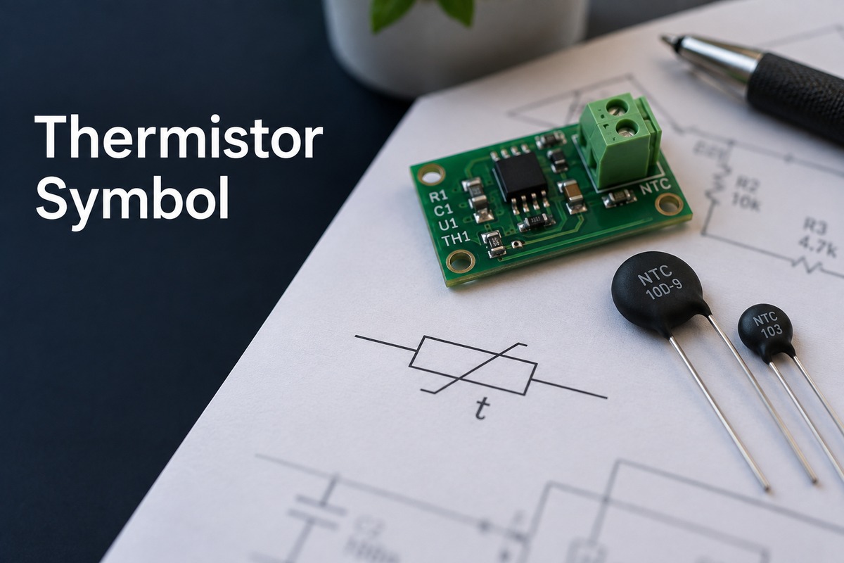

You may also like