Key Takeaways
- A conventional point-to-point LVDS link usually uses one differential termination at the receiver, commonly 100 Ω.
- The termination both develops the received differential voltage and reduces reflections by matching the transmission line.
- A representative 3.5 mA current through 100 Ω produces 350 mV; these are nominal teaching values, not universal guaranteed specifications.
- Internal termination can replace an external resistor only when the exact device, I/O bank and active configuration support it.
- Two ideal 100 Ω loads in parallel produce 50 Ω. Whether two loads are correct depends on the topology.
- AC coupling needs appropriate transmitter-side loading, receiver bias and signal behavior—not just two capacitors.
- Approve the channel using the receiver waveform and timing requirements, not a resistance reading alone.
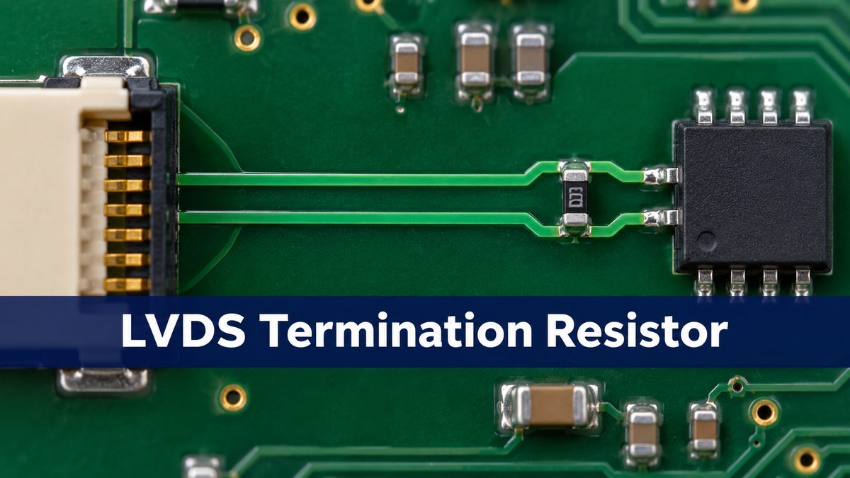
An LVDS termination resistor is a resistor connected across the two signal conductors at the receiving end of a typical LVDS link. A common value is 100 Ω, selected to match the differential transmission-line impedance and convert the driver’s steered current into a small voltage that the receiver can detect.
Getting it right involves more than selecting a 100 Ω part. The receiver may already contain termination, a connector may extend the electrical path, and AC-coupled or multipoint links need different arrangements. This guide explains the principles, calculations, connection options and PCB decisions so a schematic can become a testable design.
what is lvds
LVDS means low-voltage differential signaling: information is represented by the voltage difference between two conductors, rather than by either conductor’s voltage to ground alone. The receiver decides whether P is above or below N.
Define the differential voltage as Vdiff = VP − VN. The common-mode voltage is their average:
A positive differential voltage does not require either pin to go negative relative to ground. In an illustrative 1.2 V common-mode system, P = 1.375 V and N = 1.025 V give +350 mV differential. Swapping these levels gives −350 mV. The two states span 700 mV differential peak-to-peak—not 350 mV peak-to-peak.
Consider a hypothetical data-acquisition board carrying ADC data to an FPGA. Each lane needs an electrically compatible receiver and a defined load; successful data capture also depends on clock-to-data timing. LVDS specifies electrical signaling, not the complete data protocol. See TI’s LVDS technology overview.
lvds termination resistor
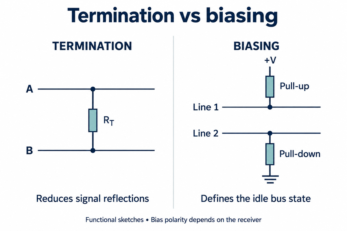
In the usual DC-coupled point-to-point circuit, the resistor connects from P to N, directly across the receiver input pair. It is not inserted in series with either conductor and is not a pull-down to ground.
The driver steers current out along one conductor, through the load, and back along the other. Reversing the current direction reverses the differential voltage. The high-impedance receiver observes that voltage while the resistor provides the intended current path.
The same resistor is the load at the end of the transmission line. Matching the load to the line helps prevent an arriving edge from reflecting back along the pair. These are related functions: replacing the resistor with an open circuit removes the intended DC load and also creates a large impedance discontinuity.
For the ADC-to-FPGA example, trace the two nets all the way through adapters and connectors before drawing the termination symbol. A resistor already on a mezzanine card is still part of the circuit. Analog Devices explains receiver-end LVDS termination.
lvds termination resistor value
The familiar 100 Ω value follows from the intended differential line impedance and the driver’s operating load. It is a common starting point, not a resistor value to apply indiscriminately to every differential interface.
A nominal current-source model gives:
TI’s LVDS Owner’s Manual uses this representative model. Actual guaranteed output levels come from the selected driver’s electrical table.
| Parameter | Value and scope |
| Differential termination | 100 Ω; common design value |
| Steered current | 3.5 mA; nominal model |
| Differential magnitude | 350 mV typical; SN65LVDS1, 100 Ω |
| Specified output magnitude | 247–454 mV; conditions below |
| Specified output common mode | 1.125–1.375 V; SN65LVDS1 |
| Nominal integrated load | 110 Ω; SN65LVDT2 only |
The SN65LVDS1 range above applies with RL = 100 Ω and 3 V ≤ VCC < 3.6 V under the datasheet’s specified conditions. At lower supply voltage, its minimum differs. The typical value is not a guaranteed minimum, and the nominal 1.2 V teaching example is not a universal input requirement. See the Rev M electrical tables.
lvds impedance matching
Match the termination to the pair’s differential characteristic impedance—not to the resistance of the copper traces. Characteristic impedance describes how a traveling wave relates voltage and current along the interconnect; a multimeter cannot measure it as a DC resistance.
For an ideal uniform line with real differential impedance Zdiff and a resistive termination RT, the load reflection coefficient is:
These calculations assume a 100 Ω line and an ideal 3.5 mA driver for the separate steady-state voltage estimate:
| Load | Load reflection | Ideal settled magnitude |
| 90 Ω | −5.26% | 315 mV |
| 100 Ω | 0% | 350 mV |
| 120 Ω | +9.09% | 420 mV |
| 50 Ω | −33.33% | 175 mV |
A positive coefficient means the reflected voltage has the same polarity as the incident wave; a negative value means opposite polarity. The percentage refers to the incident traveling voltage, not to bit-error rate or total signal loss. The settled-voltage estimate is not a prediction of the complete transition waveform.
A 120 Ω load can increase ideal settled amplitude while worsening the match to a 100 Ω line. That is why “more voltage” is not automatically better. Nonstandard values require both a device-load check and a channel assessment. The underlying reflection model is described in TI’s LVDS Application and Data Handbook.
lvds termination resistor power rating
Normal LVDS termination dissipation is small, but select the resistor using voltage across the load, not the IC supply voltage. For an ideal 350 mV differential magnitude across 100 Ω:
Both polarities produce the same resistive dissipation. Using the 700 mV differential peak-to-peak value in this formula would overestimate the ideal two-state dissipation by four times.
A 1% external resistor is a practical starting choice when the design does not specify otherwise. Its package, temperature coefficient, rated-power derating and parasitic behavior still matter. A smaller package can simplify a short, symmetric connection, but assembly capability and inspection access also constrain the choice. Calculate margin from the actual maximum operating differential voltage and resistance limits; fault conditions need a separate review.
lvds termination resistor placement
Place an external termination close to the receiver input pins, with short and balanced connections to P and N. The electrical route from the resistor to the input matters more than the distance between component outlines.
If the resistor sits beside a connector but the receiver is farther inside the board, the segment beyond the resistor becomes an unterminated branch of the intended load point. It can still disturb the receiver even though the schematic shows a correct resistor value.
For scale, assume a 20 mm post-termination segment and a propagation delay of 6 ps/mm. Its one-way delay is 120 ps and its round-trip delay is 240 ps. Against a hypothetical 500 ps edge, that is not automatically negligible. These are teaching assumptions, not a universal length limit.
Place the resistor across the incoming pair without a long tee, an asymmetric detour or an avoidable via. A selectable footprint should remain compact even when unpopulated.
lvds internal termination
Internal termination replaces the external load only when the selected receiver actually provides it in the intended operating state. “LVDS-capable input” does not by itself establish that termination is present or enabled.
For example, AMD’s DIFF_TERM documentation describes enabling built-in 100 Ω differential termination. Availability and valid conditions depend on the FPGA family, bank, I/O standard and supply requirements. Treat those conditions as part of the hardware design, not just a software detail.
| Choice | Trade-off |
| Internal load | Near input; device, bank and settings matter |
| External resistor | BOM controlled; placement and tolerance matter |
| Selectable | Flexible; document the active option |
On the ADC board, record the FPGA input standard, bank supply and active termination setting alongside the BOM population option. Check reset and configuration behavior if the ADC starts driving before the FPGA is ready. Do not infer powered internal resistance from an unpowered ohmmeter reading.
lvds double termination
A conventional single-receiver link is overterminated if an external load duplicates the intended internal load. For two ideal 100 Ω resistances at the same receiving point:
The ideal 3.5 mA model then gives 175 mV rather than 350 mV. A real driver may depart from that model, and separated loads introduce transmission-line effects. Reduced amplitude alone therefore suggests a loading problem; it does not prove one.
Establish the active receiver setting and populated components, restore the intended load, then compare measurements using the same pattern and probe setup. A different topology, such as M-LVDS, can intentionally require two terminations; “two resistors” is not a universal fault diagnosis.
lvds ac coupling termination
AC coupling blocks the transmitter’s DC common-mode voltage, allowing the receiver side to establish another bias level. It also changes the DC current paths, so it must be designed as a complete interface.
Review three things together:
- Transmitter operation: Does the driver need a DC differential load, and where is that path maintained after adding capacitors?
- Receiver bias: Is the input internally biased, or does it need an external common-mode network?
- Signal behavior: Can the clock or data tolerate startup charging and baseline movement during long intervals without transitions?
TI’s LMK00301 datasheet, AC-coupled differential operation shows arrangements that differ according to receiver termination and bias. Some maintain a driver-side DC load and accept the resulting swing reduction when a receiving load is also present. That is a designed network, not the accidental duplication discussed above.
DC-balanced data or a suitable continuous clock is easier to AC couple than an arbitrary static level. For the ADC example, consider idle patterns and clock stoppage as well as the normal stream. Do not copy a capacitor value without checking the longest transition-free interval, startup requirement and both devices’ input/output conditions.
lvds split termination
Split termination uses two resistors whose series sum provides the differential load. Two 50 Ω resistors connected from P through a midpoint to N present 100 Ω to an ideal differential signal.
The midpoint determines what else the circuit does. A capacitor from that midpoint to ground can provide a common-mode AC return. A prescribed bias network can establish a DC level in an appropriate AC-coupled implementation. A capacitor alone does not establish a DC bias because it is open at steady DC.
With equal 50 Ω resistors and identical common-mode movement on both lines, the resistors appear in parallel toward the midpoint: 25 Ω before the midpoint network. This differs from their 100 Ω differential series path. Mismatched parts or asymmetric routing can spoil that symmetry.
TI SLAA840 includes split-termination examples. Use them when the common-mode or bias requirement justifies the network; adding a midpoint capacitor is not a generic cure for poor differential routing.
lvds multidrop
One driver feeding several receivers is not the same as several devices taking turns driving a bus. Establish that distinction before deciding how many loads to fit.
| Topology | Load arrangement |
| Point-to-point LVDS | One load at receiver |
| Single-source LVDS multidrop | One far-end load; short taps |
| Multipoint M-LVDS | Both bus ends; matched devices |
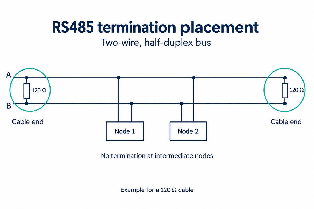
In the single-source multidrop arrangement described by TI SLAA840, the driver is at one end and the load is at the farthest receiver. Intermediate receivers must not each add another parallel termination. Their capacitance and branch lengths still affect the waveform.
M-LVDS drivers are designed for the heavier loading associated with two bus-end terminations. Two 100 Ω end loads give a 50 Ω DC equivalent, but the distributed bus is not simply a point-to-point LVDS circuit with another resistor added. Use devices and a topology intended for that service. Analog Devices AN-1177 explains the distinction.
lvds pcb layout guidelines
Route the interconnect as a controlled electrical structure, preserving its geometry and reference environment through the entire path. A correct load cannot repair an inconsistent pair.
- Impedance: derive trace width and gap from the proposed finished stackup, not another board’s nominal dimensions.
- Reference planes: keep the intended reference continuous beneath the pair; review every layer change and return-path transition.
- Symmetry: use comparable pad exits, vias, connector paths and protection on P and N.
- Stubs: keep optional footprints and test connections compact. A long measurement branch becomes part of the circuit.
- Timing: meet the device’s intra-pair and clock-to-data timing requirements without unnecessary tuning structures.
“100 Ω differential” does not mean any two individually 50 Ω routes will remain a 100 Ω pair when brought together. Coupling changes the result. Finished copper, dielectric height, pair spacing, solder mask and the nearby copper environment must agree with the impedance model.
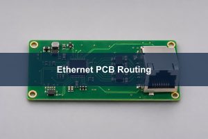
For a concrete manufacturing handoff, see the Best Technology LVDS PCB routing example; its dimensions are an example, not a universal recipe.
how to measure lvds signal on oscilloscope
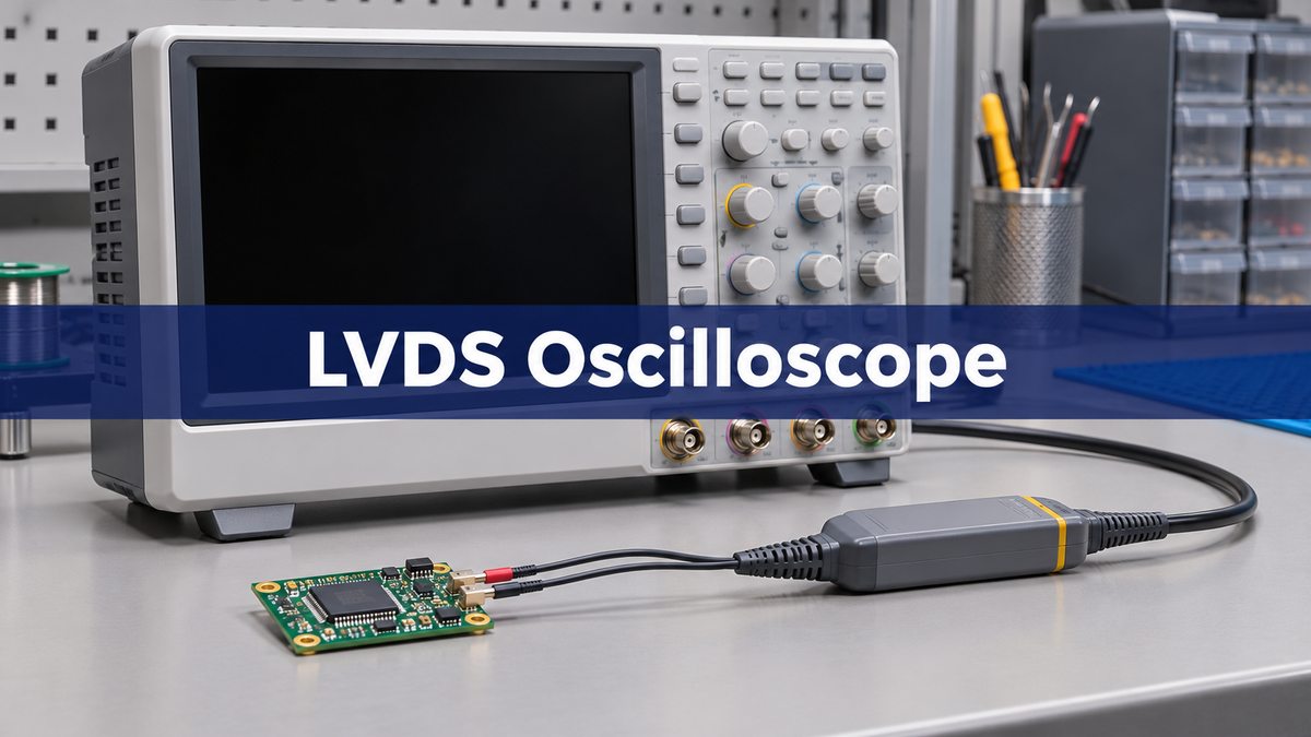
Measure the differential signal at the receiver using a suitable low-loading differential probe, and examine both amplitude and timing. A clean waveform at the transmitter does not establish what arrives at the input.
- Record the data pattern, line rate, termination state, supply condition and probe point.
- Use bandwidth appropriate to the edge speed, and keep the probe connection short and symmetric.
- Measure differential magnitude, ringing and timing; assess common mode with an appropriate setup.
- Use an eye diagram and functional error testing where the interface requirements call for them.
- Compare results with the selected devices’ input limits and the project’s timing or eye criteria.
Do not attach ordinary grounded probe clips to the signal conductors. Nor should two 50 Ω-to-ground scope inputs be assumed harmless: they can introduce another 100 Ω differential load and alter common mode. Probing can create the fault you are trying to diagnose.
Power-off resistance measurements can identify accessible passive paths when the circuit allows it. They cannot establish characteristic impedance or prove powered internal termination. A TDR coupon checks representative fabricated geometry; the receiver measurement checks the operating channel.
lvds signal integrity
Signal integrity is the combined result of loading, interconnect geometry and timing—not a property established by one resistor reading. Before manufacturing, align the schematic, layout, assembly choices and receiver configuration.
For the hypothetical ADC-to-FPGA board, the release record should identify the exact endpoints, selected input standard, intended termination and population option, approved stackup, target impedance and tolerance, timing constraints, and verification plan.
| Observed result | Useful next investigation |
| Unexpectedly low amplitude | Effective load and probe loading |
| Ringing near transitions | Stubs, connectors and impedance steps |
| Good amplitude, capture errors | Clock alignment, jitter and timing |
| Failure only at startup | Bias, reset and configuration sequence |
These are starting points, not diagnoses. Close the loop by testing the same board revision and operating conditions against defined pass criteria. If a load change improves amplitude but worsens the eye or error rate, the job is not finished.
Frequently Asked Questions
Can a 100 Ω termination make a 3.3 V transmitter compatible with a 1.8 V receiver?
Not by itself. Supply voltage and signal voltage are different quantities. Compatibility depends on differential swing, common-mode range, pin limits and the receiver’s bank rules. Termination does not replace a required level translator.
Can a short LVDS link omit the resistor?
Do not remove it just because the traces are short. A current-steering driver may still require the load to establish its output voltage. A termination-free implementation needs explicit support from the selected device documentation and validation.
Is LVDS a communication protocol like SPI?
No. LVDS describes electrical signaling. The interface still needs defined data organization, clocking and timing. Two devices can both use LVDS levels without exchanging compatible data.
Does an idle receiver automatically produce a known logic state?
No. Failsafe behavior depends on the device and the fault condition: open inputs, shorted inputs and an undriven terminated line are different cases. Select a receiver with the required behavior or use its recommended bias arrangement.
Should every unused receiver input get 100 Ω?
Not automatically. Follow the device’s unused-input instructions. A resistor across an unused input does not necessarily establish a valid logic state, while adding loads to connected bus taps can overterminate the bus.
Can an ordinary series resistor replace the parallel termination?
No. Series source termination is a different method. A resistor inserted in one or both conductors does not provide the receiving-end current path and load required by a conventional LVDS circuit.
Does a working clock prove that the data lanes are correct?
No. Each lane can have a different load, interconnect or timing relationship. Verify the affected lanes and their relationship to the sampling clock rather than approving the interface from one clock trace.
When is AC coupling the wrong starting point?
When the interface must convey a static state indefinitely, has uncontrolled long idle intervals, or lacks a defined bias and startup plan. Begin with the device-supported DC-coupled arrangement unless there is a specific reason to isolate common-mode levels.
Conclusion
For a conventional LVDS link, start with the intended differential impedance, one receiving-end load and compatible input conditions. Then make the resistor value, placement, internal configuration and PCB geometry describe the same circuit. For a Best Technology PCB fabrication discussion, send the stackup, controlled net list, impedance requirements and receiver-area routing to sales@bestpcbs.com. Bare-board manufacturing checks and complete-channel electrical validation serve different purposes; define both where the application requires them.
Technical References
- Texas Instruments: LVDS Owner’s Manual, SNLA187, 4th Edition
- Texas Instruments: SN65LVDS1 / SN65LVDS2 / SN65LVDT2, Rev M
- AMD: DIFF_TERM property and family-specific SelectIO requirements
- Texas Instruments: How to Terminate LVDS Connections with DC and AC Coupling, SLAA840
- Texas Instruments: LMK00301 AC-coupled differential termination examples
- Analog Devices: AN-1177, LVDS and M-LVDS Circuit Implementation Guide