PCB manufacturing PCB manufacturing
Home > Blog

Multi-Chip Module: Design, Packaging, Materials, and Manufacturer Guide

May 6th, 2026

A multi-chip module is an advanced electronic package that integrates two or more chips into one compact module. These chips may include logic dies, memory, RF devices, power ICs, sensors, or other semiconductor components.

Instead of mounting every chip separately on a large PCB, a multi-chip module places multiple chips close together on a shared substrate. This helps reduce signal distance, save board space, improve performance, and support higher functional density.

For engineers working on high-speed electronics, RF modules, medical devices, aerospace systems, automotive electronics, or compact embedded products, understanding multi chip module design and multi chip module packaging is becoming increasingly important.

Multi-Chip Module: Design, Packaging, Materials, and Manufacturer Guide

What Is a Multi-Chip Module?

A multi-chip module, often called an MCM, is an electronic package that contains multiple semiconductor chips inside one module. These chips are mounted on a common substrate and connected through wire bonding, flip-chip bumps, solder bumps, redistribution layers, or interposer routing.

The chips inside an MCM can perform different functions. One module may include a processor die, memory die, RF chip, sensor die, power management IC, and passive components.

In simple terms, a multi-chip module allows several chips to work together as one compact electronic unit. Compared with traditional PCB assembly, MCM packaging brings chips much closer together.

What Is a Multi-Chip Module?

How Does a Multi-Chip Module Work?

A multi-chip module works by placing several chips on a shared substrate. The substrate acts as a high-density circuit platform. It routes power, ground, clock signals, control signals, and high-speed data lines between the chips.

For example, a compact wireless module may contain an RF chip, microcontroller, memory, power management circuit, and passive matching components. These parts communicate through short internal connections instead of long PCB traces.

This shorter signal path can bring several benefits:

  • Lower signal delay
  • Better high-speed performance
  • Reduced parasitic inductance and capacitance
  • Smaller PCB footprint
  • More controlled electrical behavior
  • Higher system integration

After internal assembly, the complete MCM is mounted onto the main PCB through BGA balls, LGA pads, pins, or other package terminals.

Why Is Multi-Chip Module Packaging Used in Advanced Electronics?

Multi chip module packaging is used because advanced electronics need more functions in less space. It also helps engineers combine different semiconductor technologies in one compact structure.

A single chip may not be the best choice when different functions require different manufacturing processes. Digital logic, RF circuits, memory, power devices, and MEMS sensors may each need a different process to perform well. MCM packaging allows each chip to use the technology that suits it best.

Main advantages include:

  • Smaller size
  • Shorter interconnects
  • Flexible integration
  • Higher performance density
  • Better design modularity
  • Potential yield benefit

This is why MCM technology is widely used in processors, RF modules, aerospace electronics, medical devices, automotive radar, power modules, and compact IoT products.

Types of Multi-Chip Module Packaging

Multi-chip module packaging can be classified by substrate material and interconnection method. The common types include MCM-L, MCM-C, MCM-D, 2.5D packaging, and 3D packaging.

Types of Multi-Chip Module Packaging

MCM-L uses organic laminate substrates. It is often selected when cost, scalability, and volume production matter.

MCM-C uses ceramic substrates such as alumina or aluminum nitride. It is preferred for high-reliability, high-temperature, RF, and power applications.

MCM-D uses deposited thin-film layers to achieve very fine interconnects. It is suitable for demanding high-density and high-frequency designs.

2.5D and 3D packaging are more advanced forms of integration. They are common in high-performance computing and chiplet-based architectures.

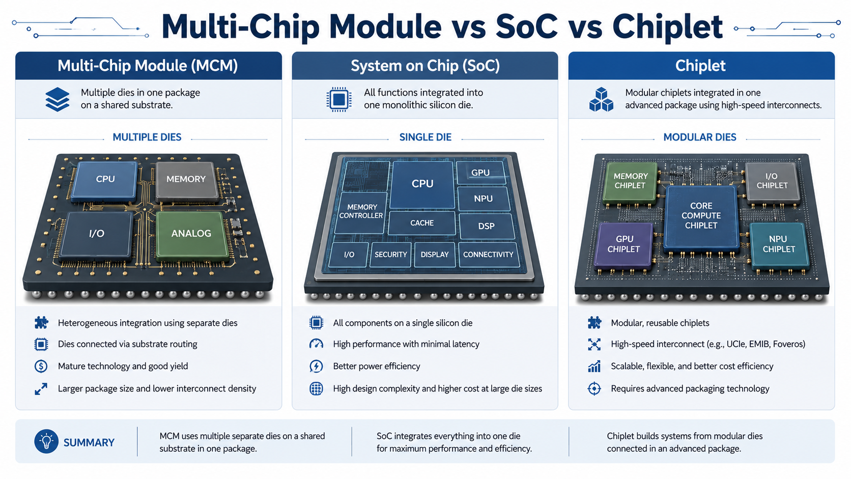
What Is the Difference Between MCM and SoC?

An MCM and an SoC both integrate multiple functions, but they do it in different ways.

An SoC, or System on Chip, integrates many functions into one single silicon die. A multi-chip module integrates multiple separate chips into one package.

ComparisonMulti-Chip ModuleSoC
StructureMultiple dies in one packageOne die with many functions
Technology flexibilityCan combine different chip processesUsually uses one semiconductor process
Design flexibilityEasier to mix and update functional diesHarder to change after chip design
Development costPractical for mixed technologiesCan be expensive for complex large dies
Yield strategyIndividual dies can be tested before assemblyOne large die may have yield challenges
Typical useRF, power, HPC, aerospace, medical modulesMCUs, processors, mobile chips, embedded ICs

An SoC is suitable when all functions can be efficiently built on one die. An MCM is often better when the product needs different chip technologies, compact size, high performance, or modular integration.

Multi-Chip Module vs Chiplet: Key Differences

The terms multi-chip module and chiplet are related, but they are not the same.

A multi-chip module is the package that contains multiple chips. A chiplet is a smaller functional die designed to work with other dies in a modular architecture.

ItemMulti-Chip ModuleChiplet
MeaningA package containing multiple chipsA small functional semiconductor die
Main rolePhysical integration platformFunctional building block
ScopeBroad packaging conceptSpecific modular chip architecture
RelationshipCan contain chipletsCan be assembled inside an MCM
ExampleRF module with several diesCPU chiplet, I/O chiplet, memory chiplet

The simplest way to understand it is this: an MCM is the package, while a chiplet is one possible building block inside that package.

Not every multi-chip module uses chiplets. For example, a ceramic RF module with amplifier dies and passive components is an MCM, but it may not be called a chiplet system.

Multi-Chip Module vs Chiplet: Key Differences

What Substrate Materials Are Used in Multi-Chip Modules?

The substrate is one of the most important parts of a multi-chip module. It affects signal routing, thermal performance, mechanical reliability, and manufacturing cost.

Common substrate materials include organic laminate, ceramic, silicon interposer, glass, and metal-based substrates.

Substrate MaterialStrengthsTypical Applications
Organic laminateCost-effective, mature, suitable for volume productionDigital modules, communication devices
CeramicHigh reliability, good thermal stability, strong insulationAerospace, RF, medical, power electronics
Silicon interposerVery fine routing and high-bandwidth connection2.5D advanced packaging
Glass substrateGood dimensional stability and electrical behaviorEmerging advanced packaging
Metal-based substrateExcellent heat spreadingPower modules and high-current applications

For cost-sensitive applications, organic laminate may be enough. For RF, medical, aerospace, and power electronics, ceramic substrates are often more suitable. For very high-density die-to-die communication, silicon interposers are commonly used.

Key Design Rules for Multi-Chip Module Design

Good multi chip module design requires more than placing several dies together. Electrical performance, thermal behavior, assembly process, material compatibility, and testing access must be considered from the beginning.

Plan the system architecture first
Before layout, define what each chip does, which chips communicate most frequently, and which signals are high-speed, noise-sensitive, or power-heavy.

Optimize die placement
Place high-speed dies close to each other. Keep heat-generating dies near effective thermal paths. For RF modules, also consider isolation, shielding, and impedance matching.

Control signal integrity
Short interconnects are helpful, but routing still matters. High-speed lines may need controlled impedance, matched lengths, clean return paths, and low-crosstalk spacing.

Design stable power distribution
Each die may need different voltage rails. Use proper decoupling, low-inductance power paths, and well-planned grounding.

Manage thermal performance
Heat can build up quickly when several dies are packed together. Thermal vias, heat spreaders, metal lids, ceramic substrates, or copper base structures may be needed.

Consider material expansion
Silicon, ceramic, organic laminate, solder, molding compound, and metal lids expand differently under temperature changes. This CTE mismatch can affect long-term reliability.

Design for manufacturability
Trace width, spacing, via structure, pad size, bonding clearance, die attach method, inspection access, and testing points must match real manufacturing capability.

A successful MCM is not only a circuit design, it is a complete packaging, material, thermal, and manufacturing project.

What Is MCM Used For?

MCM technology is used in advanced electronic systems where space, speed, reliability, or integration density matters.

Common applications include:

  • High-performance computing modules
  • AI processors and accelerator packages
  • RF and microwave modules
  • Aerospace and defense electronics
  • Medical imaging and monitoring devices
  • Automotive radar and ADAS electronics
  • Power modules
  • Wireless communication devices
  • Compact IoT modules
  • Industrial control electronics

In these applications, MCM packaging helps reduce size while improving system-level performance.

How to Choose a Multi-Chip Module Assembly Manufacturer?

Choosing the right multi-chip module assembly manufacturer is important because MCM-related projects often involve compact layouts, fine-pitch components, thermal control, stable signal paths, and strict process quality. A good manufacturer should support both assembly and early engineering review.

For compact electronic modules, RF boards, sensor modules, medical electronics, automotive control boards, industrial devices, and high-reliability PCB assemblies, EBest Circuit provides practical support from PCB fabrication to PCBA assembly and testing.

Why choose EBest Circuit?

  • Integrated PCB and PCBA service
  • Early DFM engineering review
  • Advanced PCB manufacturing capability
  • FR-4, high-Tg, HDI, rigid-flex, high-frequency, ceramic, aluminum, and copper substrate PCB support
  • Strong thermal management support
  • SMT assembly and turnkey component sourcing
  • AOI, X-ray, ICT, flying probe, functional test, and visual inspection
  • Material batch traceability and production process tracking
  • Quality documentation for high-reliability electronics projects
  • Experience in medical, automotive, industrial, communication, and aerospace-related electronics
  • Responsive engineering communication

If you are developing a compact electronic module, high-density PCB assembly, or multi-chip module-related project, you are welcome to send your Gerber files, BOM, drawings, and technical requirements to sales@bestpcbs.com for engineering review and quotation.

FAQs About Multi-Chip Module

What does multi-chip module mean?

A multi-chip module is an electronic package that integrates two or more chips into one compact module. The chips are mounted on a shared substrate and connected internally.

Is a multi-chip module the same as a chiplet?

No. A multi-chip module is the package structure. A chiplet is a small functional die that may be used inside a multi-chip package.

What is the main advantage of a multi-chip module?

The main advantage is compact integration. It can reduce board space, shorten signal paths, and improve system performance.

What is the difference between MCM and SoC?

An MCM uses multiple separate dies in one package. An SoC integrates many functions into one single silicon die.

What materials are used for MCM substrates?

Common materials include organic laminate, ceramic, silicon interposer, glass, and metal-based substrates.

Where are multi-chip modules used?

They are used in high-performance computing, RF modules, aerospace electronics, medical devices, automotive systems, power modules, and compact embedded products.

Why is ceramic used in some MCM packages?

Ceramic is used when the design needs high reliability, good thermal stability, strong insulation, and better performance in harsh environments.

How do I choose a multi-chip module assembly manufacturer?

Choose a manufacturer with engineering review capability, advanced PCB manufacturing experience, reliable assembly process, testing support, traceability control, and responsive communication. EBest Circuit supports PCB fabrication, PCBA assembly, DFM review, component sourcing, testing, and quality documentation for high-reliability electronic module projects.

You may also like

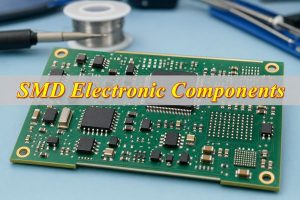
How to Identify Electronic Components on a Circuit Board?

April 29th, 2026

Have you ever stared at a circuit board and wondered how to accurately recognize the tiny parts that power every electronic device? Circuit board electronic components are the building blocks of all modern electronics, and knowing how to identify them correctly is critical for troubleshooting, maintenance, and accurate analysis. This guide breaks down every essential step, from distinguishing different component types to reading markings, testing functionality, and protecting these parts, all with practical, actionable advice to solve common pain points and avoid costly mistakes.

How to Identify Electronic Components on a Circuit Board, https://www.bestpcbs.com/blog/2026/04/how-to-identify-electronic-components-on-a-circuit-board/

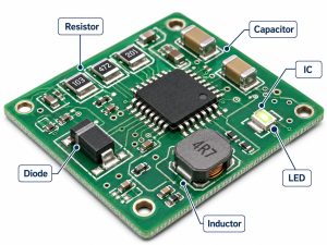
What Are the Electronic Components of a Circuit Board?

Electronic circuit board components are discrete parts that work together to enable the circuit’s functionality, each serving a specific electrical purpose. These components fall into two main categories: passive and active, with additional specialized types that support overall performance.

Passive components do not require external power to operate and are essential for regulating electrical signals. The most common passive components include resistors, which limit current flow and divide voltage; capacitors, which store and release electrical charge to filter noise and stabilize power; inductors, which store energy in magnetic fields and suppress voltage spikes; and diodes, which allow current to flow in only one direction. These components are found on every circuit board and form the foundation of basic circuit operation.

Active components require external power to function and can amplify signals or switch current. Transistors are key active components, used to amplify electrical signals and act as switches in digital circuits. Integrated circuits (ICs) are complex active components that pack hundreds or thousands of miniaturized components into a single chip, serving as the ā€œbrainā€ of the circuit for processing, control, or memory storage. Other active components include LEDs, which emit light when current passes through them, and relays, which switch high-power circuits using low-power signals.

Additional specialized components include fuses, which protect the circuit from overcurrent by melting and breaking the circuit; connectors, which link the circuit board to external devices or other boards; and switches, which control the flow of current by opening or closing the circuit. Together, these components form a cohesive system that enables the circuit board to perform its intended function, making circuit board electronic components indispensable to all electronic devices.

How to Distinguish Surface Mount and Through-Hole Circuit Board Electronic Components?

Distinguishing surface mount and through-hole circuit board electronic components is straightforward once you know their key physical and mounting characteristics. Both types serve the same electrical purposes but differ in design, mounting method, and application, with clear visual cues to tell them apart.

  • Mounting Method: Surface mount components (SMDs) are soldered directly to the surface of the circuit board, with small terminals or pads that attach to copper traces on the board’s top or bottom. Through-hole components have long metal leads that pass through holes drilled in the circuit board, with soldering done on the opposite side of the board to secure the component.

  • Size and Shape: Surface mount components are significantly smaller and flatter than through-hole components. They come in compact rectangular, square, or chip-like shapes, with no protruding leads (or very short leads). Through-hole components are larger, with cylindrical or rectangular bodies and long, thin leads that extend outward from the component.
  • Lead Configuration: Surface mount components have leads or pads along their edges or bottom, designed to sit flush against the circuit board. Through-hole components have one or more leads that extend straight out from the component body, intended to be inserted through pre-drilled holes in the board.
  • Visual Cues: Surface mount components often appear as tiny ā€œchipsā€ on the board’s surface, with no leads visible through the board. Through-hole components have leads that pass through the board, with solder joints visible on the opposite side. Older circuit boards typically use more through-hole components, while modern, compact devices rely primarily on surface mount components.
  • Application Context: Surface mount components are used in compact devices like smartphones, laptops, and wearables, where space is limited. Through-hole components are used in applications requiring high mechanical strength, such as industrial equipment, power supplies, and prototyping, where manual assembly and durability are prioritized.

How to Identify Electronic Components on a Circuit Board?

Identifying electronic components on a circuit board involves a combination of visual inspection, reading silk screen markings, and understanding component characteristics. Follow these step-by-step methods to accurately identify any component, even on dense or complex boards.

  • Check Silk Screen Markings: Most circuit boards have a silk screen layer white or gray printed text and symbols that labels each component. These labels use standard abbreviations to indicate the component type: R for resistor, C for capacitor, D for diode, Q for transistor, U for integrated circuit, L for inductor, F for fuse, and SW for switch. The label (e.g., R12, C5, U3) corresponds to the component’s position in the circuit schematic, making identification quick and accurate.
  • Recognize Physical Characteristics: Each component type has distinct physical features. Resistors are small, cylindrical (through-hole) or rectangular (surface mount) with color bands or numerical codes. Capacitors are round (electrolytic), flat (ceramic), or rectangular (film) and may have voltage or capacitance markings. Diodes have a stripe on one end indicating the cathode (negative terminal). Integrated circuits are black chips with multiple legs or pads, often with a small dot or notch marking pin 1.
  • Use Component Markings: Most components have printed markings that indicate their values, ratings, or part numbers. Resistors use color bands or 3-4 digit codes to show resistance and tolerance. Capacitors use numerical codes (e.g., 104 = 100,000 picofarads) or direct markings for capacitance and voltage. Transistors and ICs have part numbers that can be looked up to confirm their type and specifications.
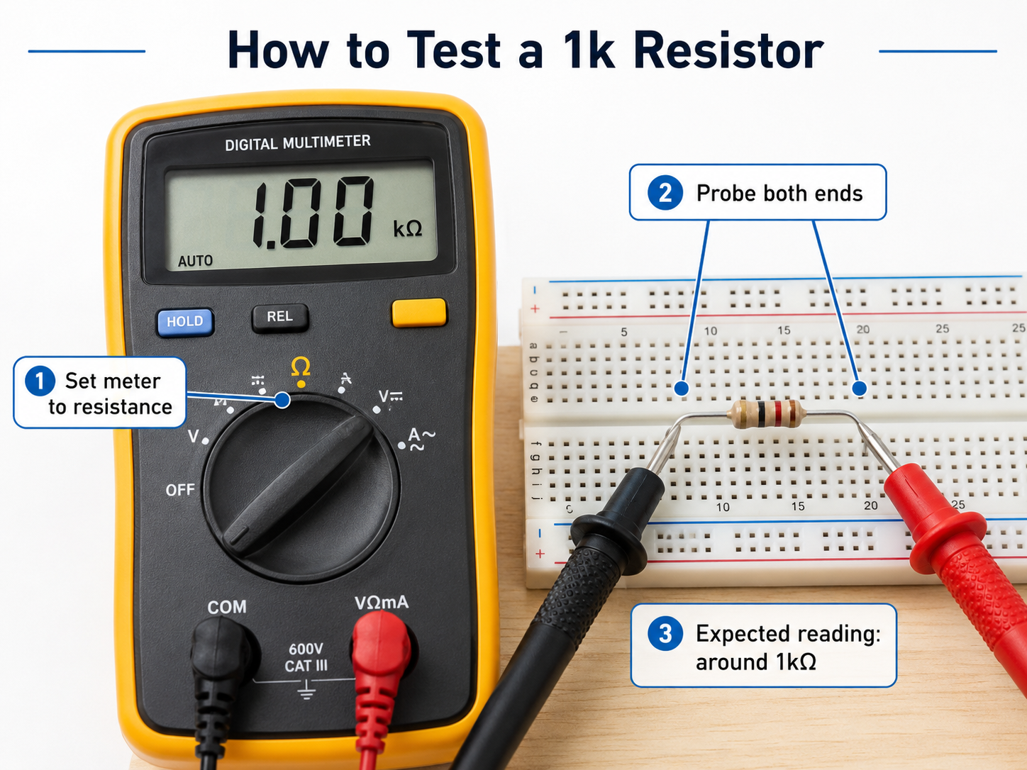
  • Verify with a Multimeter: For uncertain components, use a multimeter to test electrical properties. Resistors can be tested for resistance, capacitors for capacitance, diodes for forward/reverse bias, and transistors for continuity between pins. This step confirms the component’s type and functionality, ensuring accurate identification.
  • Cross-Reference with Schematics: If available, use the circuit board’s schematic diagram or bill of materials (BOM) to cross-reference component labels. Schematics show the component’s role in the circuit, while the BOM lists exact part numbers and specifications, eliminating guesswork.

How to Read the Markings and Codes on Circuit Board Electronic Components?

Markings and codes on circuit board electronic components provide critical information about their specifications, including value, tolerance, voltage rating, and functionality. Reading these codes correctly is essential for identifying components and ensuring they meet the circuit’s requirements, with standardized formats for each component type.

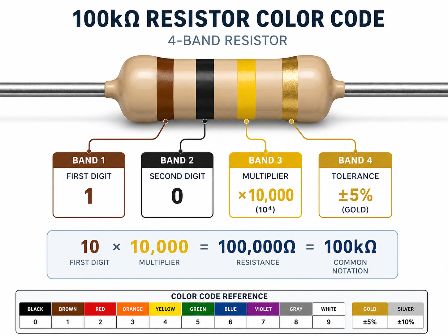
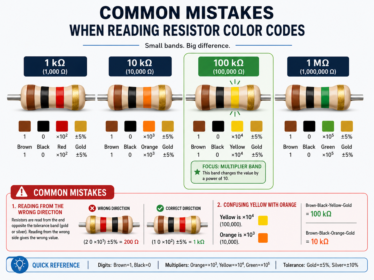
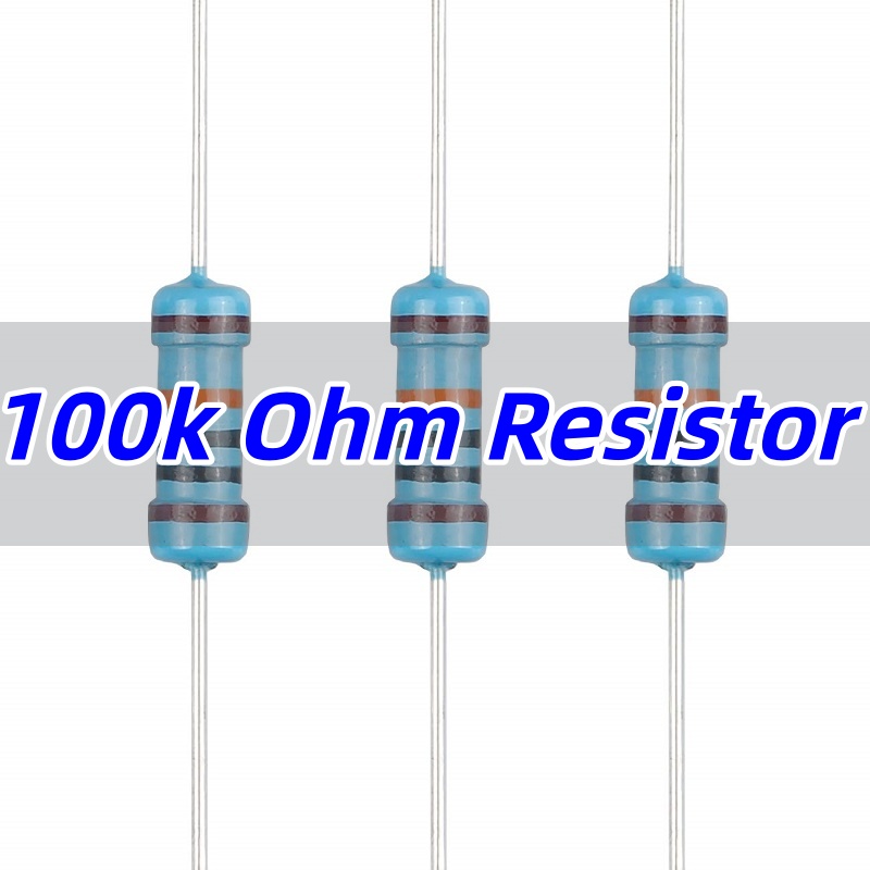
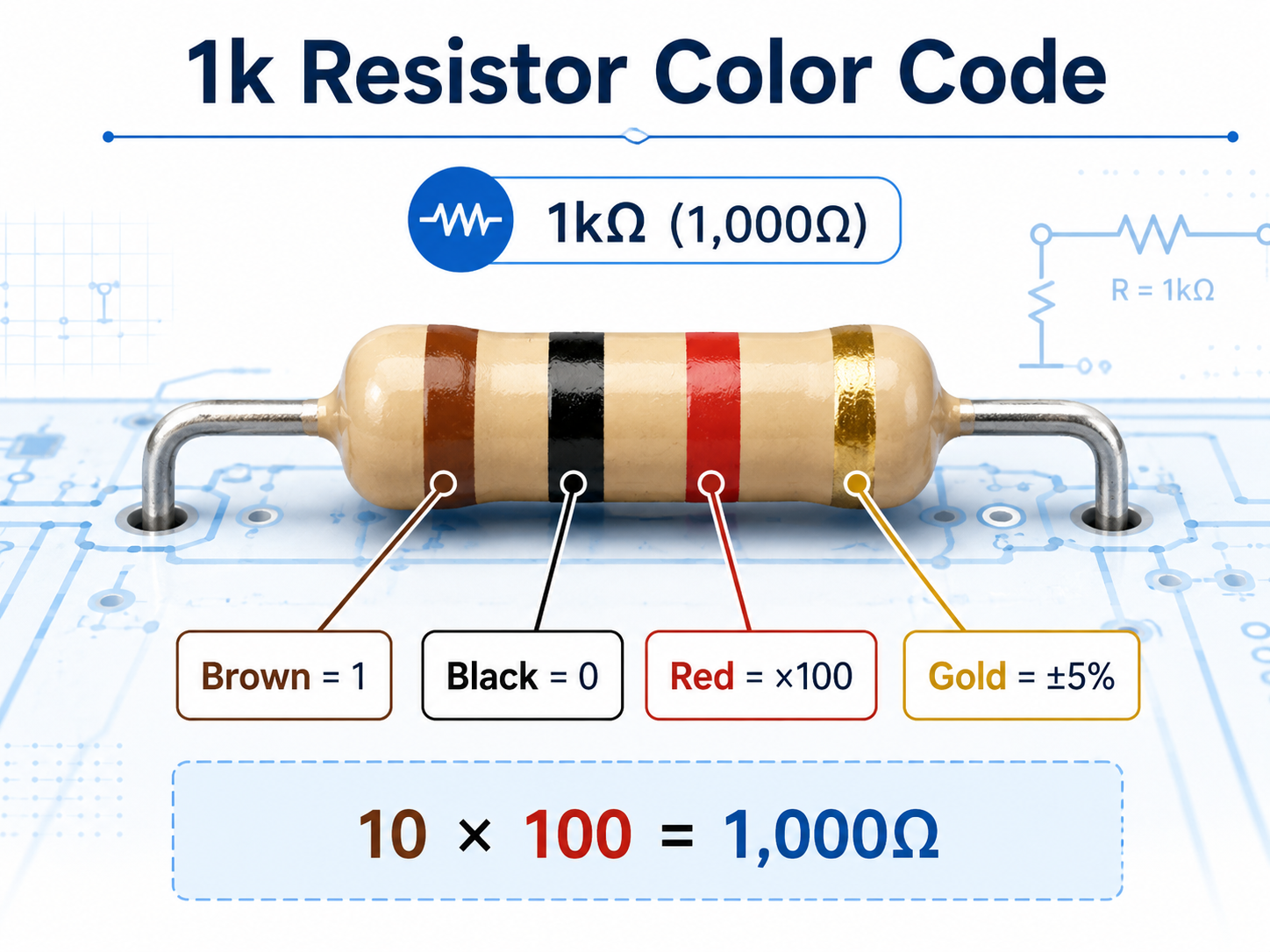
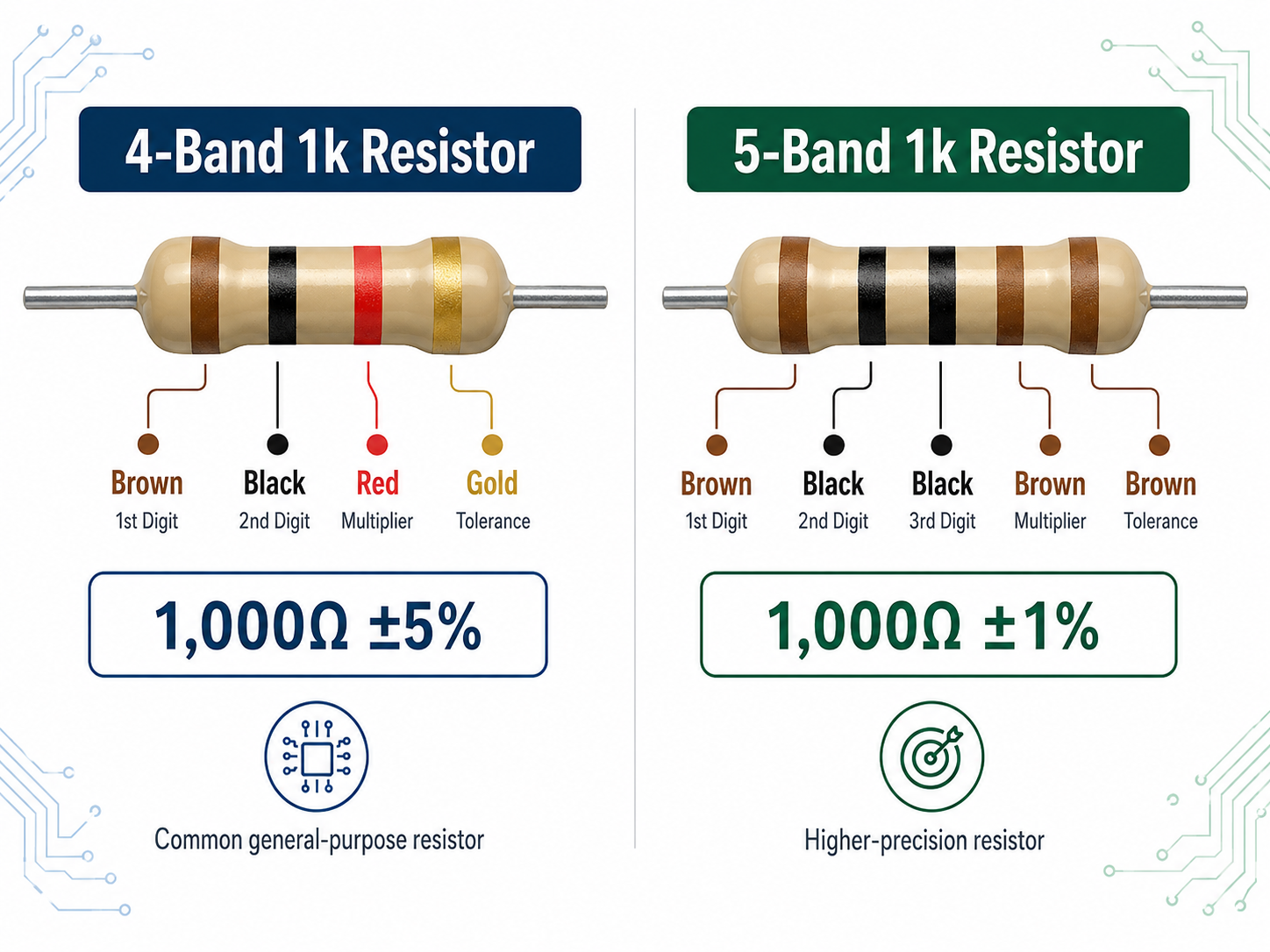
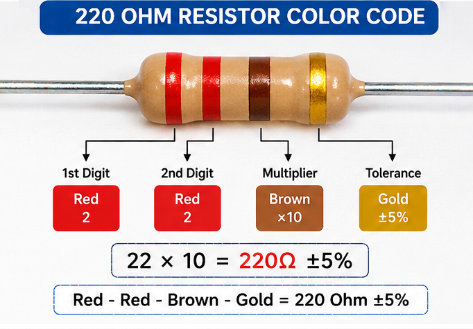
  • Resistor Markings: Through-hole resistors use color bands to indicate resistance and tolerance. The first two bands are the significant digits, the third band is the multiplier, and the fourth band (if present) is the tolerance. Surface mount resistors use 3 or 4-digit codes: 3-digit codes have two significant digits and one multiplier (e.g., 102 = 10 x 10² = 1,000 ohms), while 4-digit codes have three significant digits and one multiplier (e.g., 1002 = 100 x 10² = 10,000 ohms). Tolerance is often marked with a letter: J = ±5%, K = ±10%, M = ±20%.
  • Capacitor Markings: Capacitor markings vary by type and size. Large electrolytic capacitors directly print capacitance (e.g., 10µF) and voltage (e.g., 25V) on the body. Small surface mount capacitors use 2 or 3-digit codes: the first two digits are significant, the third is the multiplier (in picofarads), with no decimal point (e.g., 104 = 10 x 10⁓ = 100,000 pF = 100 nF). Some capacitors use letters to indicate tolerance, with J = ±5% and K = ±10% being common.
  • Diode Markings: Diodes have a single stripe on one end, which marks the cathode (negative terminal). Some diodes also have part numbers printed on the body (e.g., 1N4001), which can be looked up to confirm their type (e.g., rectifier diode) and voltage/current ratings. LEDs have a similar stripe for the cathode, with additional color markings to indicate the light color.
  • Transistor Markings: Transistors have alphanumeric part numbers (e.g., 2N2222, BC547) printed on the body. These part numbers identify the transistor type (NPN, PNP) and specifications like current, voltage, and gain. Some transistors also have a dot or notch to indicate the collector, base, or emitter pin.
  • Integrated Circuit (IC) Markings: ICs have a part number (e.g., ATmega328P, LM358) printed on the top, which identifies the chip’s functionality (e.g., microcontroller, operational amplifier). A small dot or notch on the IC marks pin 1, which is critical for proper orientation when installing or testing the component. Some ICs also include manufacturer logos or date codes.

What Tools Are Needed to Identify Electronic Circuit Board Components Accurately?

Accurate identification of electronic circuit board components requires a few essential tools, designed to enhance visibility, measure electrical properties, and verify component functionality. These tools are affordable, easy to use, and critical for avoiding misidentification and costly errors.

  • Magnifying Glass or Digital Microscope: Most circuit board electronic components are tiny, with small markings that are difficult to read with the naked eye. A magnifying glass (1020x magnification) works for basic inspection, while a digital microscope provides higher magnification and allows for detailed viewing of small surface mount components and fine markings.
  • Digital Multimeter: A multimeter is the most versatile tool for component identification. It measures resistance (for resistors), capacitance (for capacitors), voltage (for diodes and ICs), and continuity (for testing component leads). Look for a multimeter with auto-ranging functionality for ease of use, as it automatically selects the correct measurement range.
  • Component Tester: A dedicated component tester quickly identifies resistors, capacitors, diodes, transistors, and inductors by measuring their key parameters and displaying the component type and value. This tool eliminates guesswork, especially for unmarked surface mount components.
  • Gerber Viewer Software: Gerber files are used to design circuit boards, and Gerber viewer software allows users to visualize the board’s layers, component footprints, and silk screen markings. This tool helps cross-reference component labels with their physical positions on the board, useful for complex or dense circuits.
  • Soldering Iron and Desoldering Tool: For components that need to be removed for closer inspection or testing, a soldering iron (2530W for surface mount, 4060W for through-hole) and desoldering tool (solder sucker or desoldering braid) are essential. These tools allow safe removal of components without damaging the circuit board or the component itself.
  • Flashlight or Task Light: Proper lighting is critical for visual inspection. A bright, focused flashlight or task light illuminates small components and markings, making it easier to read silk screen labels and component codes, especially on dark or densely populated circuit boards.

How to Identify Faulty Circuit Board Electronic Components During Identification?

Identifying faulty circuit board electronic components during inspection involves recognizing visual signs of damage and using tools to test functionality. Faulty components often show clear physical indicators, and simple tests can confirm whether a component is working correctly, saving time in troubleshooting.

  • Visual Inspection for Physical Damage: Look for obvious signs of damage, such as burnt or discolored components (common in resistors and ICs), bulging or leaking capacitors (electrolytic capacitors often bulge when faulty), cracked component bodies, or broken leads. These visual cues indicate a faulty component that needs replacement.
  • Test for Continuity: Use a multimeter in continuity mode to check for broken leads or internal damage. A component with broken leads will show no continuity, while a faulty resistor or diode may show inconsistent continuity. For example, a diode should show continuity in one direction only; continuity in both directions indicates a faulty diode.
  • Measure Component Values: Compare the measured value of a component to its marked value. A resistor with a measured resistance significantly higher or lower than its marked value is faulty. A capacitor with a measured capacitance below 80% of its marked value is likely faulty and should be replaced.
  • Check for Overheating: During operation, touch components (carefully to avoid burns) to feel for excessive heat. Components that are abnormally hot (beyond their normal operating temperature) are likely faulty, as overheating indicates internal damage or incorrect operation.
  • Inspect Solder Joints: Faulty solder joints (cold solder, bridging, or poor adhesion) can cause components to function incorrectly. Look for solder joints that are dull, cracked, or not fully covering the component lead and circuit board pad. These joints can be reflowed with a soldering iron to restore connectivity.
  • Cross-Reference with Circuit Behavior: If the circuit is not functioning as intended, cross-reference the component’s role in the schematic with the observed behavior. For example, a non-functional LED may indicate a faulty resistor (limiting current) or a faulty LED itself. Testing the component’s value will confirm which is faulty.
Circuit board electronic components, https://www.bestpcbs.com/blog/2026/04/how-to-identify-electronic-components-on-a-circuit-board/

How to Test Electronic Components on a Circuit Board?

Testing electronic components on a circuit board ensures they function correctly and meet the circuit’s specifications. The testing process varies by component type but follows a consistent, step-by-step approach using basic tools, with clear pass/fail criteria for each component.

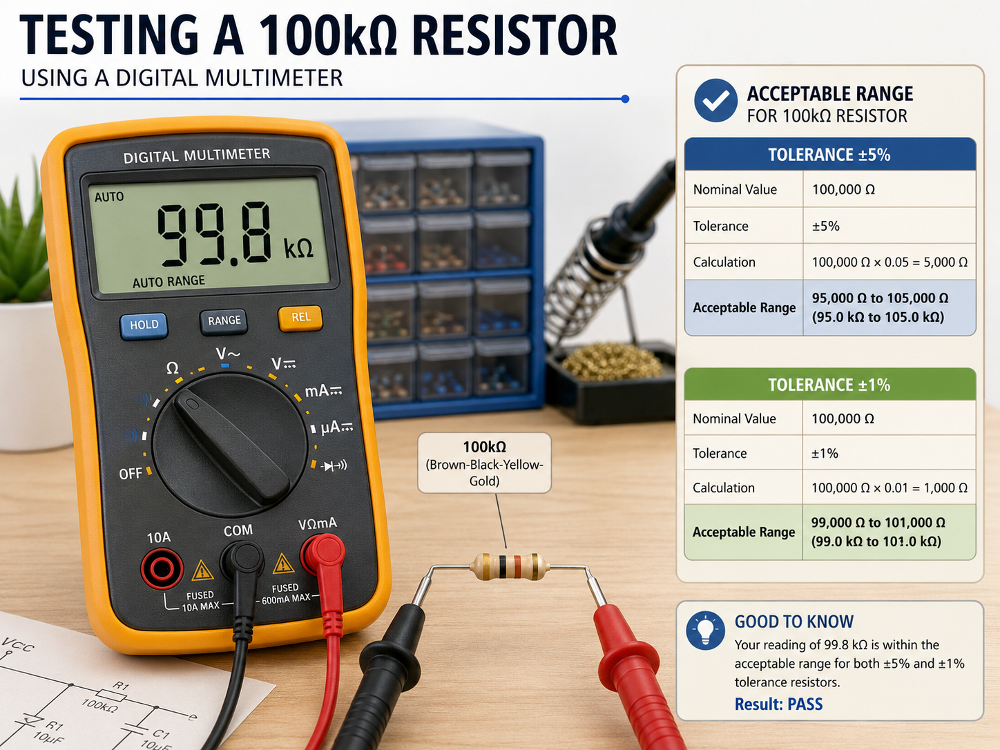
  • Resistor Testing: Set the multimeter to resistance mode (ohms). Touch the multimeter probes to the resistor’s leads (no need to remove the resistor from the board if it is not in parallel with other components). Compare the measured resistance to the resistor’s marked value. A measured value within the component’s tolerance (±5%, ±10%, or ±20%) indicates a working resistor; a value outside this range means the resistor is faulty.
  • Capacitor Testing: Set the multimeter to capacitance mode. For large electrolytic capacitors, discharge them first (use a resistor to discharge stored charge). Touch the probes to the capacitor’s terminals (match positive to positive, negative to negative for polarized capacitors). A measured capacitance within 10-20% of the marked value is acceptable; values significantly lower indicate a faulty capacitor.
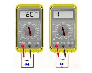
  • Diode Testing: Set the multimeter to diode mode. Touch the positive probe to the diode’s anode (no stripe) and the negative probe to the cathode (stripe). A working diode will show a voltage drop (0.5-0.7V for silicon diodes). Reverse the probes, no voltage drop should be displayed. If voltage is displayed in both directions or no voltage is displayed in either direction, the diode is faulty.
  • Transistor Testing: For NPN transistors, set the multimeter to diode mode. Touch the positive probe to the base and the negative probe to the emitter, this should show a voltage drop. Touch the positive probe to the base and the negative probe to the collector, another voltage drop should be displayed. Reverse the probes for PNP transistors. No voltage drop in either test indicates a faulty transistor.
  • Integrated Circuit (IC) Testing: Testing ICs requires a multimeter and knowledge of the chip’s pinout (from the datasheet). Measure the voltage at the power pins (VCC and GND) to ensure the IC is receiving power. Check the output pins against the expected voltage (from the schematic). If the IC is not receiving power or the output is incorrect, the IC is likely faulty. For more detailed testing, use an IC tester or oscilloscope.
  • Inductor Testing: Set the multimeter to resistance mode. Touch the probes to the inductor’s leads. A working inductor will show low resistance (near zero ohms). High resistance or no continuity indicates a broken inductor coil, which is faulty.
Circuit Board Electronic Components, https://www.bestpcbs.com/blog/2026/04/how-to-identify-electronic-components-on-a-circuit-board/

How to Remove Electronic Components from a Circuit Board?

Removing electronic components from a circuit board requires care to avoid damaging the board, the component (if reuse is needed), and surrounding components. The process varies slightly for surface mount and through-hole components, but follows consistent best practices to ensure safe removal.

  • Prepare the Workspace: Ensure the circuit board is disconnected from power and any external devices. Use an anti-static mat and anti-static wristband to prevent electrostatic discharge (ESD) damage to sensitive components. Gather the necessary tools: soldering iron, desoldering tool (solder sucker or desoldering braid), tweezers, and a magnifying glass.
  • Removing Through-Hole Components: Heat the solder joint on one lead of the component with the soldering iron. Once the solder melts, use the desoldering sucker to remove the molten solder. Repeat for the other lead(s). Once all solder is removed, gently pull the component’s leads through the board using tweezers. If solder remains in the holes, use the desoldering braid to remove it.
  • Removing Surface Mount Components: Use a soldering iron with a fine tip or a hot air station (preferred for small components). For components with multiple leads (e.g., ICs), heat all leads simultaneously with the hot air station (set to 300350°C) until the solder melts. For single-lead components (e.g., resistors, capacitors), heat one lead at a time, using tweezers to lift the component once the solder melts. Avoid applying excessive heat, as this can damage the circuit board’s copper traces.
  • Clean the Solder Pads: After removing the component, use desoldering braid to clean any remaining solder from the circuit board’s pads. This ensures the pads are flat and free of debris, making it easier to install a new component if needed.
  • Inspect for Damage: After removal, inspect the circuit board for damaged copper traces or pads. If a trace is lifted or damaged, use a soldering iron to reattach it (if possible) or use a jumper wire to restore connectivity. Inspect the removed component for damage if reuse is intended.
  • Handle Components Carefully: Use tweezers to handle components, avoiding direct contact with the leads or pins. This prevents ESD damage and contamination from oils on the hands, which can affect component performance.

How to Avoid Damaging Circuit Board Electronic Components During Identification?

Damaging circuit board electronic components during identification is a common mistake that can lead to costly repairs or component failure. Following these simple steps ensures components and the circuit board remain intact during inspection, testing, and handling.

  • Use Anti-Static Protection: Electrostatic discharge (ESD) can damage sensitive components like ICs and transistors. Always use an anti-static mat and anti-static wristband when handling the circuit board and components. Avoid touching component pins or leads directly with bare hands, as oils and static can cause damage.
  • Avoid Excessive Heat: When using a soldering iron or hot air station, set the temperature to the minimum required (300350°C for surface mount components, 4060°C for through-hole). Excessive heat can melt component bodies, damage circuit board traces, or cause internal component failure. Limit heat exposure to 510 seconds per solder joint.
  • Use the Right Tools: Avoid using sharp tools (e.g., screwdrivers, knives) to pry components, as this can damage leads, pins, or circuit board pads. Use tweezers with fine tips for handling small components, and a magnifying glass to avoid accidental contact with surrounding components.
  • Do Not Force Components: If a component does not lift easily after desoldering, do not force it. Reheat the solder joints to ensure all solder is melted, and check for any hidden solder bridges that may be holding the component in place. Forcing components can break leads or lift copper traces.
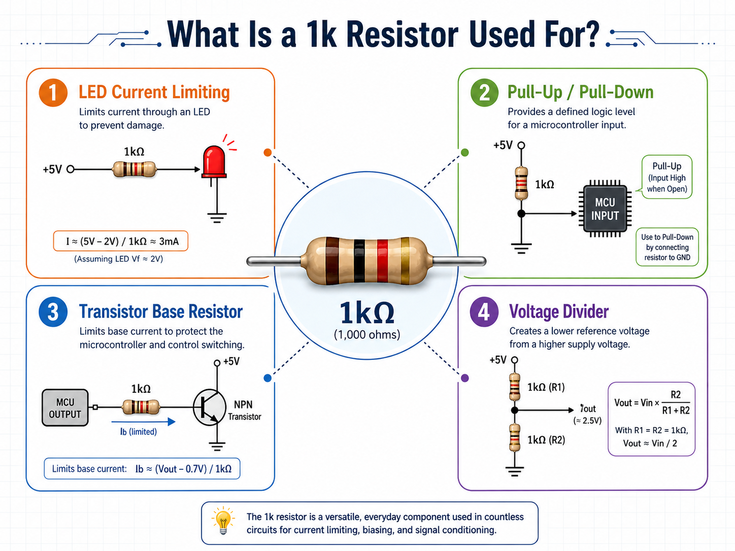
  • Discharge Capacitors Before Testing: Capacitors store electrical charge even after the circuit is disconnected from power. Discharge them using a resistor (1k10k ohms) before testing or removing them, as stored charge can cause electric shock or damage to the multimeter.
  • Keep the Workspace Clean: A cluttered workspace increases the risk of dropping tools or components onto the circuit board, causing physical damage. Keep tools organized and the workspace free of debris, and use a soft mat to place the circuit board on to prevent scratches.
Circuit board electronic components, https://www.bestpcbs.com/blog/2026/04/how-to-identify-electronic-components-on-a-circuit-board/

How to Protect Electronic Components on a Circuit Board?

Protecting electronic components on a circuit board ensures long-term reliability and prevents damage from environmental factors, ESD, and physical wear. Proper protection methods vary by application but focus on shielding components from harm while maintaining their functionality.

  • Apply Conformal Coating: Conformal coating is a thin, protective layer applied to the circuit board and components to shield them from moisture, dust, chemicals, and temperature variations. Common coating materials include acrylic (easy to remove, good for general protection), silicone (excellent heat resistance), and polyurethane (high chemical resistance). The coating is applied evenly, covering all components without blocking connectors or heat sinks.
  • Use Heat Sinks: Components that generate significant heat (e.g., ICs, power transistors) require heat sinks to dissipate heat and prevent overheating. Heat sinks are attached to the component’s body using thermal paste, which improves heat transfer. Choose a heat sink size appropriate for the component’s power dissipation to ensure effective cooling.
  • Implement ESD Protection: Install ESD protection components (e.g., TVS diodes, varistors) on the circuit board to divert static charge away from sensitive components. Use anti-static packaging for components during storage and transportation, and ensure the circuit board is grounded during assembly and operation.
  • Protect Against Overcurrent and Overvoltage: Use fuses or circuit breakers to protect components from overcurrent, which can cause overheating and damage. Install voltage regulators or Zener diodes to prevent overvoltage, which can destroy sensitive components like ICs and transistors. These components act as a safety net, breaking the circuit or regulating voltage when limits are exceeded.
  • Secure Components with Potting Compound: For circuit boards used in harsh environments (e.g., industrial, automotive), potting compound is poured over the board and components to provide complete protection from moisture, vibration, and physical damage. Potting compound is a rigid or flexible material that encapsulates the board, forming a protective barrier.
  • Proper Storage and Handling: Store circuit boards in a dry, cool environment, away from direct sunlight and moisture. Use anti-static bags for individual boards or components, and avoid stacking boards to prevent physical damage. When handling, use anti-static protection and avoid touching component pins or leads.

FAQs About Electronic Components on a Circuit Board

Q1: Can I identify circuit board electronic components without removing them from the board?

A1: Yes, most circuit board electronic components can be identified without removal. Use silk screen markings to determine component type, visual cues to recognize physical characteristics, and a multimeter to test electrical properties. For unmarked components, use a component tester or cross-reference with the circuit schematic to confirm identification.

Q2: Why do some surface mount components have no markings?

A2: Small surface mount components (e.g., 0402 or 0201 size resistors and capacitors) often have no markings due to their tiny size. Manufacturers mark the reels holding these components instead of individual parts. To identify unmarked surface mount components, use a component tester to measure their values or cross-reference with the circuit’s BOM or schematic.

Q3: How do I know if a capacitor on a circuit board is faulty?

A3: Faulty capacitors often show visual signs like bulging, leaking, or discoloration. To confirm, use a multimeter to measure capacitance. A capacitor with a measured value below 80% of its marked value is faulty. Additionally, capacitors that overheat during operation or cause circuit malfunctions (e.g., voltage fluctuations) are likely faulty and should be replaced.

Q4: What is the difference between passive and active electronic circuit board components?

A4: Passive components do not require external power to operate and include resistors, capacitors, inductors, and diodes. They regulate electrical signals but do not amplify or switch current. Active components require external power and include transistors, ICs, LEDs, and relays. They amplify signals, switch current, or perform complex processing tasks.

Q5: How can I avoid ESD damage when working with circuit board electronic components?

A5: To avoid ESD damage, use an anti-static mat and anti-static wristband to ground yourself and the circuit board. Avoid touching component pins or leads with bare hands, and store components in anti-static bags. Ensure the workspace is free of static-generating materials (e.g., plastic, fabric) and ground all tools used during inspection and testing.

You may also like

How to Test a Diode with a Multimeter?

April 29th, 2026

Do you struggle to accurately test a diode and determine if it’s functioning properly, or wonder why your diode test results are inconsistent even when using a multimeter?

Testing a diode is a fundamental skill for anyone working with electronic circuits, as a faulty diode can cause signal distortion, energy loss, or complete circuit failure.

This guide breaks down every step of diode testing with a multimeter, addresses common pain points, and provides clear, actionable instructions to ensure reliable results every time.

Whether using a digital or analog multimeter, or even testing without a dedicated diode tester function, you’ll learn the exact techniques to verify diode performance, identify damage, and avoid costly mistakes.

How to Test a Diode with a Multimeter, https://www.bestpcbs.com/blog/2026/04/how-to-test-a-diode-with-a-multimeter/

What Tool is Used to Test a Diode?

The primary tool for testing a diode is a multimeter, available in two main types. Both digital and analog multimeters can perform a diode test, though digital models often have a dedicated function for greater accuracy. Below are the two types of multimeters used for diode testing, along with their key features and typical use cases:

  • Digital Multimeter: It comes with a dedicated diode test mode, a digital display for precise voltage and resistance readings, auto-ranging options, and a low battery indicator. It is the most common tool for diode testing, ideal for quick and accurate results with minimal interpretation.
  • Analog Multimeter: It features a needle display, manual range selection, and uses an internal battery for resistance measurements. It does not have a dedicated diode mode and instead uses the resistance mode for testing. It is suitable for basic diode testing when a digital multimeter is unavailable, though it requires more interpretation of readings.

What is the Symbol for Diode Test on Multimeter?

The diode test symbol on a multimeter is standardized across most models, making it easy to identify once you know what to look for. The symbol varies slightly between digital and analog multimeters but follows the same core design.

  • Digital Multimeter: The diode test symbol is typically a triangle pointing to a vertical line. This symbol directly represents the diode’s structure, where the triangle is the anode and the vertical line is the cathode. It is often labeled ā€œDIODEā€ or ā€œDIā€ next to the symbol for clarity. On some models, this symbol shares a position with the continuity test (represented by a sound wave icon), so you may need to press a function button to switch between continuity and diode test modes.
  • Analog Multimeter: Analog models rarely have a dedicated diode test symbol because they use the resistance mode for diode testing. Instead, look for the resistance symbol (Ī©) to select the appropriate range for testing. The resistance symbol is a horseshoe-shaped icon, and you will need to choose a low resistance range (typically RƗ10 or RƗ100) for accurate diode readings.

How to Prepare a Multimeter Before You Test a Diode?

Proper preparation of a multimeter is critical to ensure accurate diode test results and avoid damage to the multimeter or the diode. Follow these steps to prepare your multimeter before starting any diode test.

  • Check the multimeter battery: Ensure the multimeter has a fully charged battery. A low battery can cause inaccurate readings, especially in resistance or diode test modes. For analog multimeters, a weak battery may prevent the needle from reaching full scale during zero adjustment, leading to false readings. Replace the battery if the low battery indicator lights up (digital models) or if the needle fails to respond properly (analog models).
  • Inspect test leads: Examine the multimeter test leads for any damage, such as frayed wires or cracked insulation. Damaged leads can cause poor contact, leading to inconsistent or incorrect readings. Ensure the leads are securely connected to the multimeter’s input jacks, red lead to the positive (+) jack and black lead to the negative (-) or common (COM) jack.
  • Set the multimeter to the correct mode: For digital multimeters, turn the dial to the diode test mode (marked with the diode symbol). For analog multimeters, set the dial to the resistance mode (Ī©) and select a low range (RƗ10 or RƗ100). Avoid using high resistance ranges, as they may not provide enough current to forward-bias the diode.
  • Zero the analog multimeter (if applicable): For analog models, short the two test leads together (touch the metal tips) and turn the zero adjustment knob until the needle points to 0Ī© on the resistance scale. This step calibrates the multimeter for accurate resistance readings and is essential for reliable diode testing. Digital multimeters do not require manual zeroing.
  • Disconnect power from the circuit: If testing a diode that is still in a circuit, turn off all power sources connected to the circuit. This includes batteries, power supplies, and any other voltage sources. Even low voltage can interfere with the diode test and pose a safety hazard. Additionally, discharge any capacitors in the circuit, as they can hold a charge and cause false readings or damage the multimeter.

How to Identify the Anode and Cathode When Testing a Diode With a Multimeter?

Identifying the anode (positive terminal) and cathode (negative terminal) of a diode is essential for accurate testing, as diodes only conduct current in one direction. A diode test will only yield meaningful results if the multimeter leads are connected correctly to the anode and cathode. Use these methods to identify the terminals.

  • Check the diode’s physical markings: Most diodes have a visible band or line near one end, this band indicates the cathode. The end with the band is the cathode, and the opposite end is the anode. This marking is universal and applies to most diode types, including rectifier diodes, zener diodes, and Schottky diodes. For small signal diodes, the band may be small but still visible with a magnifying glass if needed.
  • Use the multimeter’s diode test mode (digital models): Set the digital multimeter to diode test mode, then touch the red lead to one end of the diode and the black lead to the other. If the multimeter displays a voltage drop (typically 0.5–0.8V for silicon diodes), the red lead is connected to the anode and the black lead to the cathode. If the display shows ā€œOLā€ (overload), reverse the leads, the red lead will now be on the cathode and the black lead on the anode.
  • Use resistance mode (analog or digital multimeters): Set the multimeter to a low resistance range. Touch the red lead to one end of the diode and the black lead to the other. A low resistance reading (100Ω–10kĪ©) indicates the diode is forward-biased, meaning the red lead is on the anode and the black lead on the cathode. A high resistance reading (infinite or ā€œOLā€) indicates reverse bias, meaning the leads are connected to the cathode and anode respectively.
  • Refer to the diode’s datasheet: If the physical markings are unclear or missing, consult the diode’s datasheet. The datasheet will include a diagram of the diode’s pinout, clearly labeling the anode and cathode. This is especially useful for specialized diodes, such as LEDs or zener diodes, which may have unique packaging.

How to Test a Diode With a Digital Multimeter?

Testing a diode with a digital multimeter is straightforward, thanks to the dedicated diode test mode that provides precise readings. Follow these steps to perform a accurate diode test with a digital multimeter.

  • Prepare the multimeter: Follow the preparation steps outlined earlier—check the battery, inspect test leads, set the dial to the diode test mode, and ensure the circuit (if applicable) is powered off and capacitors are discharged.
  • Identify the diode’s anode and cathode: Use the physical markings or multimeter method to determine which end is the anode and which is the cathode.
  • Connect the test leads: Touch the red multimeter lead to the diode’s anode and the black lead to the diode’s cathode. This forward-biases the diode, allowing current to flow if the diode is functional.
  • Record the reading: A functional silicon diode will display a voltage drop between 0.5V and 0.8V. Germanium diodes will display a lower voltage drop, between 0.2V and 0.3V. This voltage drop is a key indicator of a healthy diode, as it confirms the diode is conducting current in the forward direction.
  • Reverse the test leads: Touch the red lead to the cathode and the black lead to the anode. This reverse-biases the diode, which should block current flow.
  • Record the second reading: A healthy diode will display ā€œOLā€ (overload) or a very high resistance value (infinite) when reverse-biased. This indicates the diode is blocking current in the reverse direction, as it should.
  • Interpret the results: Compare the two readings to determine if the diode is functional. A good diode will show a voltage drop in forward bias and ā€œOLā€ in reverse bias. Any deviation from this pattern indicates a faulty diode.
How to Test a Diode With a Digital Multimeter, https://www.bestpcbs.com/blog/2026/04/how-to-test-a-diode-with-a-multimeter/

How to Test a Diode With an Analog Multimeter Correctly?

Analog multimeters do not have a dedicated diode test mode, so they use the resistance mode to test diodes. This requires careful range selection and interpretation of the needle position. Follow these steps to correctly test a diode with an analog multimeter.

  • Prepare the multimeter: Check the battery, inspect test leads, set the dial to the resistance mode (Ī©), and select a low range (RƗ10 or RƗ100). Short the test leads together and adjust the zero adjustment knob until the needle points to 0Ī© on the resistance scale.
  • Identify the diode’s anode and cathode: Use the physical markings or resistance test method to determine the diode’s terminals.
  • Connect the test leads (forward bias): Touch the black lead to the diode’s anode and the red lead to the cathode. Note that analog multimeters have reverse polarity in resistance mode, the black lead is connected to the internal battery’s positive terminal, while the red lead is connected to the negative terminal. This is opposite to digital multimeters, so correct lead placement is critical.
  • Record the needle position: A healthy diode will show a low resistance reading, with the needle deflecting significantly toward the 0Ī© end of the scale. The exact resistance value will vary by diode type and multimeter range, but it should be consistent with the diode’s specifications (typically 100Ω–10kĪ© for silicon diodes on RƗ10 range).
  • Reverse the test leads (reverse bias): Touch the black lead to the cathode and the red lead to the anode. This reverse-biases the diode.
  • Record the second needle position: A healthy diode will show a very high resistance reading, with the needle remaining near the infinite (āˆž) end of the scale. This indicates the diode is blocking current in the reverse direction.
  • Interpret the results: A functional diode will have a low resistance in forward bias and high resistance in reverse bias. If the needle shows the same reading in both directions, or no deflection at all, the diode is faulty. Note that analog multimeter readings are less precise than digital ones, so focus on the relative difference between forward and reverse resistance.

How to Test a Diode Without a Diode Tester Using a Multimeter?

Many multimeters, especially older analog models or basic digital models, do not have a dedicated diode tester function. However, you can still test a diode using the multimeter’s resistance mode. This method is reliable and works for all diode types, as long as you follow the correct steps.

  • Prepare the multimeter: Set the multimeter to the resistance mode (Ī©) and select a low range (RƗ10 or RƗ100 for analog models; 200Ī© or 2kĪ© for digital models). For analog multimeters, zero the device by shorting the test leads and adjusting the zero knob.
  • Disconnect the diode from the circuit: If the diode is in a circuit, remove one end to avoid interference from other components. This ensures the reading reflects only the diode’s resistance, not the entire circuit.
  • Test forward bias resistance: Connect the test leads to the diode’s anode and cathode (follow polarity rules for your multimeter type). For digital multimeters, red lead to anode and black lead to cathode; for analog multimeters, black lead to anode and red lead to cathode. A healthy diode will show a low resistance reading (100Ω–10kĪ©).
  • Test reverse bias resistance: Reverse the test leads so the diode is reverse-biased. A healthy diode will show a very high resistance reading (infinite or ā€œOLā€ on digital models).
  • Verify with voltage drop (digital multimeters only): If your digital multimeter has a voltage mode, you can verify the diode’s functionality by measuring the forward voltage drop. Set the multimeter to DC voltage mode (2V range), connect the red lead to the anode and black lead to the cathode, and apply a small forward current (using a battery if needed). A reading of 0.5–0.8V (silicon) or 0.2–0.3V (germanium) confirms the diode is functional.
  • Interpret the results: The key is to compare the forward and reverse resistance readings. A functional diode will have a significant difference between the two—low forward resistance and high reverse resistance. If the readings are similar or both are high/low, the diode is faulty.

How Many Ohms Should a Diode Read When Testing With a Multimeter?

The resistance reading of a diode when tested with a multimeter depends on whether the diode is forward-biased or reverse-biased, as well as the type of diode (silicon, germanium) and the multimeter’s range. There is no single ā€œcorrectā€ ohm value, but there are standard ranges that indicate a healthy diode.

For forward-biased diodes, the resistance reading varies by diode type.Silicon diodes, the most common type, typically read between100Ī© and 10kĪ© when tested on a low resistance range (RƗ10 or RƗ100 for analog multimeters, 200Ī© or 2kĪ© for digital multimeters). This range is due to the diode’s forward voltage drop of 0.5–0.8V, which limits the current flow and results in a moderate resistance reading.

Germanium diodes have a lower forward voltage drop (0.2–0.3V), so their forward resistance reading is lower, typically between 50Ī© and 5kĪ©. This is because the lower voltage drop allows more current to flow, reducing the measured resistance.

For reverse-biased diodes, the resistance reading should be very high—effectively infinite. On digital multimeters, this is displayed as ā€œOLā€ (overload). On analog multimeters, the needle will remain near theinfinite (āˆž) end of the scale. A reverse resistance reading that is low or close to the forward resistance reading indicates a faulty diode, as it is not blocking current in the reverse direction.

It is important to note that the exact resistance reading can vary based on the multimeter’s range. Using a higher resistance range (e.g., RƗ1k for analog multimeters) will result in a higher forward resistance reading, while a lower range will result in a lower reading. The key is not the exact value, but the difference between forward and reverse resistance, a healthy diode will have a large difference between the two.

How to Check If a Diode Is Damaged With a Multimeter?

Checking if a diode is damaged with a multimeter follows a step-by-step process, focusing on verifying the diode’s one-way conductivity (the core feature of a functional diode). Below are the clear, actionable steps to detect damage, with key details and fault types highlighted for easy reading (no H3 titles, directly listed):

  • Prepare the Multimeter and Diode: Before testing, ensure accurate results by completing these preparations: Set the multimeter to the correct mode (digital: diode test mode; analog: resistance mode (Ī©), low range RƗ10 or RƗ100); for analog multimeters, zero the device (short test leads and adjust zero knob to 0Ī©, digital does not need this); isolate the diode (disconnect one end from circuit if applicable, turn off power and discharge capacitors); inspect test leads for damage and ensure secure connection to correct jacks (red to positive (+), black to common (COM)).
  • Identify the Diode’s Anode and Cathode: Correct lead placement is critical (diodes conduct only one way). Use one of these methods: Check physical markings (most diodes have avisible band/line near the cathode, opposite end is anode); use a digital multimeter (diode test mode: touch red to one end, black to the other—0.5–0.8V for silicon means red is anode, black is cathode; ā€œOLā€ means reverse leads).
  • Test Forward Bias (Conduction Check): Test if the diode conducts current correctly (anode to cathode). Connect test leads properly: Digital multimeter – Red lead to anode, black lead to cathode; Analog multimeter – Black lead to anode, red lead to cathode (reverse polarity in resistance mode). Record the reading: Digital – healthy silicon diode shows 0.5–0.8V (germanium: 0.2–0.3V); Analog – needle deflects significantly toward 0Ī© (100Ω–10kĪ© for silicon on RƗ10 range).
  • Test Reverse Bias (Blockage Check): Test if the diode blocks current (one-way valve function). Reverse the test leads: Digital – red to cathode, black to anode; Analog – black to cathode, red to anode. Record the second reading: Digital – healthy diode shows ā€œOLā€ (overload) (infinite resistance); Analog – needle remains near infinite (āˆž) end of the scale.
  • Interpret Results to Identify Damage: Compare forward and reverse readings—deviations indicate damage. Common damage types: • Open Circuit Damage: Reading is ā€œOLā€ (digital) or infinite resistance (analog) in both forward and reverse bias; means the diode cannot conduct current at all (caused by excessive voltage/current burning the semiconductor). • Short Circuit Damage: Reading is low resistance (or voltage drop near 0V on digital diode mode) in both forward and reverse bias; means the diode acts like a wire (caused by voltage spikes or physical damage, risks damaging other components). • Leakage Damage (Partial Damage): Reverse resistance is lower than normal (e.g., 100kĪ© instead of infinite), forward reading is normal; means the diode allows some reverse current (causes signal distortion/power loss, due to age, overheating, or manufacturing defects).
  • Confirm Damage (Optional Verification): For extra certainty: Repeat forward and reverse tests 2–3 times (inconsistent readings = poor contact or partial damage); for digital multimeters, use voltage mode (2V range) to measure forward voltage drop (readings outside 0.5–0.8V silicon/0.2–0.3V germanium = damage); for zener diodes, reverse bias should show zener voltage (not ā€œOLā€)—if not, zener is damaged.
  • Key Takeaway: A healthy diode has a clear difference between forward (low resistance/voltage drop) and reverse (high resistance/OL) readings. Any deviation means the diode is damaged and should be replaced.
How to Check If a Diode Is Damaged With a Multimeter, https://www.bestpcbs.com/blog/2026/04/how-to-test-a-diode-with-a-multimeter/

Can You Test a Diode in Circuit When Using a Multimeter?

Testing a diode in circuit is possible, but it isnot always reliable. The presence of other components in the circuit, such as resistors, capacitors, or other diodes, can interfere with the multimeter’s readings, leading to false results. In most cases, it is best to remove the diode from the circuit for accurate testing.

If testing in circuit is necessary, follow these precautions to minimize interference. First, turn off all power to the circuit and discharge any capacitors. Capacitors can hold a charge and cause false readings or damage the multimeter. Next, identify the diode’s terminals and ensure no other components are connected directly across the diode—parallel resistors or other diodes can bypass the diode being tested, leading to incorrect resistance or voltage drop readings.

When testing in circuit with a digital multimeter in diode test mode, a healthy diode will still show a voltage drop of 0.5–0.8V (silicon) in forward bias and ā€œOLā€ in reverse bias, provided no other components are interfering. If the reading is inconsistent or does not match the expected values, the interference from other components is likely the cause.

Analog multimeters are more prone to interference when testing in circuit, as their resistance readings are affected by parallel components. A resistor in parallel with the diode will lower the measured resistance, making a healthy diode appear faulty. For this reason, analog multimeters are not recommended for in-circuit diode testing unless the diode is isolated from other components.

In summary, while in-circuit testing is possible for quick checks,removing the diode from the circuit is the only way to ensure accurate results. This is especially important when diagnosing a faulty circuit, as false readings can lead to incorrect component replacement and further issues.

What Are the Common Mistakes When Testing a Diode With a Multimeter?

Even experienced technicians make mistakes when testing diodes, leading to incorrect results and wasted time. Avoid these common mistakes to ensure accurate diode test results every time.

  • Incorrect lead polarity: Connecting the multimeter leads to the wrong diode terminals (anode and cathode) will result in reverse bias when forward bias is intended, and vice versa. This leads to false readings, such as ā€œOLā€ in forward bias or a low resistance in reverse bias. Always double-check the diode’s terminals before connecting the leads.
  • Testing a diode in a powered circuit: Forgetting to turn off power to the circuit or discharge capacitors can cause interference with the multimeter reading and pose a safety hazard. Even low voltage can affect the diode test, leading to false results. Always ensure the circuit is powered off and capacitors are discharged before testing.
  • Using the wrong multimeter mode or range: For digital multimeters, using resistance mode instead of diode test mode can lead to inaccurate voltage drop readings. For analog multimeters, using a high resistance range (e.g., RƗ1k) can result in no visible needle deflection, making it impossible to interpret the reading. Always use the correct mode and range for diode testing.
  • Not zeroing the analog multimeter: Failing to zero the analog multimeter before testing leads to inaccurate resistance readings. This is a common mistake that can make a healthy diode appear faulty or vice versa. Always short the test leads and adjust the zero knob before starting resistance-based diode tests.
  • Ignoring diode type differences: Silicon and germanium diodes have different forward voltage drops and resistance readings. Assuming all diodes have the same specifications can lead to incorrect interpretations. Always consider the diode type when evaluating test results.
  • Testing a diode in circuit without isolating it: As discussed earlier, other components in the circuit can interfere with the multimeter reading. Testing a diode without removing it from the circuit can lead to false results, especially if there are parallel resistors or capacitors.
  • Using damaged test leads: Frayed or damaged test leads can cause poor contact, leading to inconsistent or incorrect readings. Always inspect the test leads before use and replace them if they are damaged.
Testing a Diode With a Multimeter, https://www.bestpcbs.com/blog/2026/04/how-to-test-a-diode-with-a-multimeter/

FAQs About Diode Testing

Q1: Can a multimeter test all types of diodes, including LEDs and zener diodes?

A1: Yes, a multimeter can test all types of diodes, including LEDs, zener diodes, Schottky diodes, and rectifier diodes. The testing process is similar for all types, but there are minor differences. For LEDs, a forward voltage drop of 1.8–2.2V is normal (higher than silicon diodes). For zener diodes, reverse bias testing will show a voltage drop equal to the zener voltage (e.g., 5V for a 5V zener diode) instead of ā€œOL.ā€

Q2: Why does my multimeter show different resistance readings for the same diode when using different ranges?

A2: Diodes are nonlinear components, meaning their resistance changes with the voltage and current applied. When using different multimeter ranges, the internal voltage and current of the multimeter change, leading to different resistance readings. This is normal—focus on the difference between forward and reverse resistance, not the exact value.

Q3: What if my digital multimeter does not have a diode test mode?

A3: If your digital multimeter does not have a dedicated diode test mode, use the resistance mode (200Ī© or 2kĪ© range) to test the diode. Follow the same steps as testing without a diode tester—check forward and reverse resistance. You can also use the voltage mode to measure the forward voltage drop, which is a more accurate indicator of diode functionality.

Q4: How do I know if a diode is a silicon or germanium type?

A4: The easiest way to distinguish between silicon and germanium diodes is by their forward voltage drop. Silicon diodes have a forward voltage drop of 0.5–0.8V, while germanium diodes have a drop of 0.2–0.3V. Use a digital multimeter in diode test mode to measure the forward voltage drop and identify the diode type.

Q5: Can a diode be partially damaged, or is it either good or bad?

A5: Diodes can be partially damaged, most commonly as leaky diodes. A leaky diode allows some reverse current to flow but not enough to be considered a short circuit. This can cause subtle issues in the circuit, such as signal distortion or power loss. Testing both forward and reverse bias will reveal leakage, as the reverse resistance will be lower than normal.

You may also like

Which Is Good, Polarized vs Non-Polarized Capacitor?

April 29th, 2026

When designing circuits or selecting components for a project, many people wonder which is good, polarized vs non-polarized capacitor. Choosing the wrong type can lead to circuit failure, component damage, or even safety hazards.

This article breaks down the core differences, uses, symbols, and selection criteria for polarized and non-polarized capacitors, providing clear, actionable information to help you make the right choice every time.

Whether you’re working on a power supply circuit, audio equipment, or high-frequency applications, understanding polarized vs non-polarized capacitor is critical to ensuring circuit reliability and performance.

Polarized vs Non-Polarized Capacitor, https://www.bestpcbs.com/blog/2026/04/polarized-vs-non-polarized-capacitor/

What Is a Polarized and Non-Polarized Capacitor?

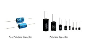
A polarized capacitor is a type of capacitor with distinct positive and negative terminals that must be connected in a specific orientation to function properly. Its internal structure is asymmetric, typically using an electrochemically grown oxide layer as the dielectric.

Common types include aluminum electrolytic and tantalum capacitors. The dielectric layer forms only under a specific voltage polarity during manufacturing, so reversing the connection causes the dielectric to break down, leading to overheating, leakage, or even component failure.

A non-polarized capacitor, also known as a bipolar capacitor, has no fixed positive or negative terminals and can be connected in any direction in a circuit. Its internal structure is symmetric, with identical electrodes and dielectric materials on both sides.

This design allows it to handle bidirectional current flow, making it suitable for circuits where voltage polarity changes regularly. Common types include ceramic, film, and mica capacitors, which are valued for their stability across different frequencies and temperatures.

What Is the Symbol of a Polarized and Non-Polarized Capacitor?

The symbols of polarized and non-polarized capacitors are clearly distinguishable, reflecting their polarity differences. Here is a detailed comparison:

Polarized Capacitor Symbol: Its symbol has clear positive and negative markings. It has two parallel lines representing capacitor plates, with one shorter line marked with a minus sign for the negative terminal and the longer line for the positive terminal.

Electrolytic and tantalum capacitors may have a curved line on the negative side to highlight polarity. This design ensures correct installation in DC circuits, as their dielectric layer only stabilizes under specific voltage polarity.

Non-Polarized Capacitor Symbol: It has no polarity markings and consists of two equal-length parallel lines with no distinction between positive and negative terminals. Its symmetric design matches its symmetric internal structure, allowing bidirectional current flow.

Ceramic, film and mica capacitors all use this standard symbol, making them easy to identify in circuit schematics, especially in AC or high-frequency circuits.

Polarized vs Non-Polarized Capacitor, https://www.bestpcbs.com/blog/2026/04/polarized-vs-non-polarized-capacitor/

What Are Polarized and Non-Polarized Capacitors Used for?

Capacitors are essential for storing charge, filtering signals, and coupling circuits, but polarized and non-polarized capacitors are tailored to different application scenarios based on their structural differences. Their uses are distinct and closely tied to their polarity characteristics and performance advantages.

Polarized capacitorsare mainly used in DC circuits, leveraging their high capacitance advantage to store large amounts of electrical energy efficiently. They are widely applied in power supply filtering to smooth voltage fluctuations and reduce ripple, bulk energy storage for circuits needing sudden power bursts, and low-frequency signal coupling in audio amplifiers. Tantalum polarized capacitors, with their compact size, are also commonly used in small electronic devices like mobile phones and laptops.

Non-polarized capacitors, by contrast, are suitable for both AC and DC circuits, especially scenarios where voltage polarity changes regularly. Their excellent frequency stability and low equivalent series resistance make them ideal for high-frequency filtering, signal coupling (to separate AC and DC signals), oscillation circuits, and audio crossovers. Ceramic non-polarized capacitors are preferred for high-frequency applications, while film non-polarized capacitors are favored in audio circuits for low distortion.

What Is the Difference Between a Polarized and Non-Polarized Capacitor?

Comparison PointPolarized CapacitorNon-Polarized Capacitor
Polarity RequirementMust be connected with correct positive and negative orientation; reverse connection causes failureNo polarity requirement; can be connected in any direction
Capacitance RangeHigher capacitance (typically µF to thousands of µF) for bulk energy storageLower capacitance (typically pF to µF) for signal and high-frequency tasks
Voltage RatingLower voltage ratings (usually up to ~100V) due to delicate dielectric layerHigher voltage ratings (up to several kV) for AC and high-voltage circuits
Equivalent Series Resistance (ESR)Higher ESR, which can cause heat generation in high-current circuitsLower ESR, making them more efficient in high-frequency applications
Temperature StabilityLess stable; performance degrades with temperature changes and agingBetter stability; consistent performance across a wide temperature range
Physical SizeLarger for similar capacitance due to internal structureSmaller for lower capacitance; compact design for high-frequency use
Failure ModeReverse connection, overvoltage, or aging can cause leakage, overheating, or ruptureRare failure; typically only fails due to extreme overvoltage or physical damage
Polarized vs Non-Polarized Capacitor, https://www.bestpcbs.com/blog/2026/04/polarized-vs-non-polarized-capacitor/

Which Is Safer to Use, Polarized vs Non-Polarized Capacitor?

Non-polarized capacitors are generally safer to use than polarized capacitors. Non-polarized capacitors have no polarity requirement, so there is no risk of reverse connection.

Their symmetric structure and stable dielectric materials make them less likely to fail catastrophically. Even if exposed to moderate overvoltage, they typically break down without causing fire, leakage, or explosion.

Polarized capacitors pose greater safety risks if not used correctly. Reverse connection causes the dielectric layer to dissolve, leading to high current flow, heat buildup, and potential component rupture.

Aluminum electrolytic capacitors may leak electrolyte when damaged, while tantalum polarized capacitors can catch fire if reverse-biased or exposed to excessive voltage. Proper installation with correct polarity and adherence to voltage ratings are essential to ensure safety when using polarized capacitors.

Are Non-Polarized Capacitors More Reliable Than Polarized Ones?

Non-polarized capacitors are generally more reliable than polarized capacitors in most circuit applications. Their symmetric design and lack of polarity requirement eliminate the risk of reverse connection failure, one of the most common causes of capacitor damage.

They also have better temperature stability and lower ESR, which reduces wear and tear over time.

Polarized capacitors are less reliable due to their internal structure. Aluminum electrolytic capacitors use liquid or gel electrolytes that evaporate over time, leading to reduced capacitance, increased ESR, and eventual failure.

Tantalum polarized capacitors are sensitive to surge currents and reverse voltage, which can cause permanent short circuits. Both types degrade faster in high-temperature environments, further reducing their reliability.

However, polarized capacitors are still reliable when used within their specifications and in circuits with stable DC voltage.

Which Has Higher Capacitance, Polarized vs Non-Polarized Capacitor?

Polarized capacitors have significantly higher capacitance than non-polarized capacitors. Polarized capacitors achieve high capacitance by using an extremely thin electrochemically grown oxide layer as the dielectric.

This thin dielectric allows for more charge storage in a compact space, with capacitance values ranging from microfarads to thousands of microfarads.

Non-polarized capacitors have lower capacitance due to their symmetric structure and thicker dielectric materials. Most non-polarized capacitors have capacitance values in the picofarad to microfarad range.

Achieving high capacitance with non-polarized capacitors would require a much larger physical size, making them impractical for applications that need bulk energy storage. For example, a 1000 µF polarized capacitor is compact, while a non-polarized capacitor with the same capacitance would be significantly larger and more expensive.

Which Is Cheaper, Polarized vs Non-Polarized Capacitor?

Polarized capacitors are generally cheaper than non-polarized capacitors, especially for high capacitance values. Aluminum electrolytic polarized capacitors are mass-produced and use low-cost materials, making them the most affordable option for bulk energy storage.

A 1000 µF aluminum electrolytic capacitor typically costs a few cents, making it ideal for cost-sensitive projects.

Non-polarized capacitors are more expensive, especially for higher capacitance or specialized applications. Ceramic non-polarized capacitors are affordable for low capacitance values, but film and mica non-polarized capacitors cost more due to their higher quality materials and manufacturing processes.

A non-polarized capacitor with the same capacitance as a polarized one can cost 10 to 20 times more. For example, a 1000 µF film non-polarized capacitor may cost $5 to $20, compared to $0.10 to $0.50 for an equivalent aluminum electrolytic polarized capacitor.

Which Is Good, Polarized vs Non-Polarized Capacitor?

There is no universal answer to which is good, polarized vs non-polarized capacitor, the right choice depends on the circuit requirements. Polarized capacitors are better for DC circuits that require high capacitance and bulk energy storage.

They are ideal for power supply filtering, low-frequency signal coupling, and applications where space is limited but high capacitance is needed. They are also cheaper, making them suitable for cost-sensitive projects.

Non-polarized capacitors are better for AC circuits, high-frequency applications, and circuits where voltage polarity changes. They are safer, more reliable, and have better temperature stability, making them ideal for signal coupling, high-frequency filtering, and oscillation circuits.

They are the best choice when polarity cannot be guaranteed or when circuit stability is a top priority. Understanding the specific needs of your circuit, such as voltage type, capacitance requirements, and environmental conditions is key to choosing between polarized vs non-polarized capacitor.

Polarized vs Non-Polarized Capacitor, https://www.bestpcbs.com/blog/2026/04/polarized-vs-non-polarized-capacitor/

How to Tell if a Capacitor Is Polarized or Non-Polarized?

Identifying whether a capacitor is polarized or non-polarized is critical to avoid circuit damage and ensure proper performance. Below are simple, non-repetitive methods to distinguish the two types:

  • Check polarity markings: Polarized capacitors have clear positive and negative indicators, such as a minus sign on the body, a longer lead for the positive terminal, an arrow pointing to the negative terminal (film types), or a plus sign (supercapacitors). Non-polarized capacitors have no such markings.
  • Examine component shape: Aluminum electrolytic polarized capacitors are cylindrical with a ribbed negative side and an explosion-proof slot. Tantalum polarized capacitors are small and rectangular with polarity markings. Non-polarized capacitors are usually small, flat, and uniform with no terminal distinction.
  • Review capacitor type: Aluminum electrolytic, tantalum, and conductive polymer capacitors are almost always polarized. Ceramic, film, and mica capacitors are nearly always non-polarized, with rare high-frequency ceramic exceptions needing datasheet confirmation.
  • Inspect circuit schematic: Polarized capacitors have a symbol with a minus sign on one side. Non-polarized capacitors have two equal-length parallel lines with no polarity indicators.
  • Check pin length and color: Through-hole polarized capacitors traditionally have a longer positive pin and shorter negative pin. Some film polarized capacitors use red pins for positive and black for negative.
  • Use a multimeter: Measure resistance in both directions. Polarized capacitors show significantly different resistance values forward and reverse. Non-polarized capacitors show nearly the same resistance (usually infinite) in both directions.
  • Refer to the capacitor model: Search the model number in manufacturer manuals or online databases, which clearly indicate polarity and terminal positions, useful for capacitors with unclear markings.
  • Observe circuit application: Capacitors for DC circuit filtering, bulk energy storage, or low-frequency coupling are usually polarized. Those for AC circuits, high-frequency filtering, or oscillation are usually non-polarized.

Can You Use a Non-Polarized Capacitor Instead of a Polarized One?

Yes, you can use a non-polarized capacitor instead of a polarized one, but only if you meet specific requirements. The non-polarized capacitor must have the same or higher capacitance value and voltage rating as the polarized capacitor it is replacing.

This ensures it can handle the same amount of charge and voltage as the original component.

However, there are practical limitations to consider. Non-polarized capacitors with high capacitance are larger and more expensive than polarized capacitors, making them impractical for many projects.

For example, replacing a 1000 µF polarized capacitor with a non-polarized one would require a much larger component, which may not fit in the circuit layout. Additionally, non-polarized capacitors have lower capacitance density, so they may not be suitable for applications that require high capacitance in a compact space.

When replacing a polarized capacitor with a non-polarized one, always check the datasheet to ensure compatibility with the circuit’s requirements.

FAQs About Polarized vs Non-Polarized Capacitor

Q1: Can Polarized Capacitors Be Used in AC Circuits?

A1: No, polarized capacitors cannot be used in AC circuits. Their dielectric layer is designed for DC voltage only; alternating polarity will break down the dielectric, causing overheating, leakage, and component failure. Non-polarized capacitors are designed for AC circuits and should be used instead.

Q2: What Happens if You Reverse a Polarized Capacitor?

A2: Reversing a polarized capacitor dissolves its dielectric layer, leading to high current flow and heat buildup. This can cause electrolyte leakage, component rupture, or even fire (especially with tantalum capacitors). Always check polarity markings before installation to avoid this issue.

Q3: Are Non-Polarized Capacitors Suitable for DC Circuits?

A3: Yes, non-polarized capacitors can be used in DC circuits for filtering, decoupling, and signal coupling. However, their lower capacitance makes them unsuitable for bulk energy storage, where polarized capacitors are more practical.

Q4: How Long Do Polarized vs Non-Polarized Capacitors Last?

A4: Non-polarized capacitors have a longer lifespan (10–20 years) due to their stable structure. Polarized capacitors last 2–10 years, as their liquid/gel electrolytes evaporate over time. High temperatures accelerate aging for both types, so proper heat management is key.

Q5: Which Type of Capacitor Is Better for High-Frequency Circuits?

A5: Non-polarized capacitors are better for high-frequency circuits. Their low equivalent series resistance (ESR) and strong temperature stability ensure reliable performance, with ceramic non-polarized capacitors being the top choice for minimal signal loss.

Q6: How to Verify Polarized Capacitor Polarity When Markings Are Blurred?

A6: For aluminum electrolytic capacitors, use the diode mode on a multimeter: connect the red test lead to one terminal and the black test lead to the other. If it shows 0.5–1V (gradually increasing to OL), the red test lead is connected to the positive terminal; swapping the test leads shows OL or a higher voltage. This is an auxiliary method, replace old capacitors with unclear markings for safety.

Q7: Are All Ceramic and Film Capacitors Non-Polarized?

A7: Almost all ceramic and film capacitors (such as polyester capacitors and polypropylene capacitors) are non-polarized and can be connected in any direction. Only a few high-frequency ceramic capacitors may have directional requirements, which need confirmation via datasheets.

You may also like

How to Choose Current Limiting Resistor for LED?

April 28th, 2026

When designing LED circuits, many professionals struggle with selecting the right current limiting resistor to protect LEDs and ensure stable performance, but what exactly is a current limiting resistor and how do you choose the correct one for your LED application? This blog breaks down every critical detail, from definitions and working principles to calculation methods and practical selection tips, addressing common pain points and providing actionable guidance to help you avoid costly mistakes and build reliable circuits.

Current Limiting Resistor, https://www.bestpcbs.com/blog/2026/04/current-limiting-resistor/

What is a Current Limiting Resistor?

A current limiting resistor is a passive two-terminal electronic component designed to control the amount of electric current flowing through a circuit. It restricts current to a safe, predetermined level by introducing a specific amount of electrical resistance, preventing excessive current that could damage sensitive components like LEDs.

Also known as a limiting resistor, it operates based on Ohm’s Law, converting excess electrical energy into heat that dissipates safely into the surrounding environment. Unlike other resistors, its primary function is not just to adjust signal levels or divide voltage but to act as a protective barrier.

It is available in various forms, including carbon film, metal film, and wire wound, each suited to different current and power requirements. The key distinction lies in its application: it is specifically sized to limit current rather than serve general circuit tuning purposes.

What is the Symbol of Current Limiting Resistors?

Current limiting resistors use the same standard symbols as all fixed resistors, as their function is a specific application of general resistor technology. Two primary symbols are used globally, aligned with international standards.

The ANSI style symbol features a rectangular box with two leads extending from either side, representing the resistor’s body and connection points.

The IEC symbol, more commonly used in European and global circuits, is a simple zigzag line with leads on both ends, visually depicting the resistance path that restricts current flow.

These symbols are identical for all fixed resistors because the current limiting function is determined by the resistor’s value and placement in the circuit, not its physical design or symbol. When reading schematics, look for either symbol in series with an LED to identify the component responsible for current control.

What is the Purpose of a Current Limiting Resistor?

The core purpose of a current limiting resistor is to restrict electrical current to a safe level for the components in a circuit. It prevents overcurrent conditions that can cause overheating, component failure, or permanent damage.

For sensitive components like LEDs, this protection is critical, as they have strict current tolerances that, when exceeded, lead to immediate burnout. Beyond protection, it stabilizes circuit performance.

It ensures consistent current flow even when there are minor fluctuations in input voltage, maintaining uniform brightness in LEDs and preventing erratic behavior. It also absorbs excess voltage in circuits where the power supply voltage exceeds the component’s required operating voltage, converting the excess into heat to keep the circuit within safe parameters.

Additionally, it acts as a simple, cost-effective short circuit protection mechanism. In the event of a component short, the limiting resistor restricts the maximum current in the circuit, protecting the power supply and other components from damage.


How Does a Current Limiting Resistor Work?

A current limiting resistor works by leveraging Ohm’s Law, which states that current (I) is equal to voltage (V) divided by resistance (R), or I = V/R. When connected in series with an LED or other component, it increases the total resistance of the circuit, thereby reducing the total current flowing through the loop.

In a typical LED circuit, the power supply provides a fixed voltage, while the LED has a specific forward voltage drop, the voltage required to turn it on. The current limiting resistor is sized to absorb the difference between the supply voltage and the LED’s forward voltage, restricting the current to the LED’s safe operating level.

For example, if a 5V power supply is used with an LED that has a 2V forward voltage drop, the resistor absorbs the remaining 3V. By selecting the correct resistance value, the current is limited to the LED’s rated level, typically 10 to 20mA for standard LEDs. The resistor dissipates the excess energy as heat, which is why power rating is a critical consideration when selecting the component.

When to Use a Current Limiting Resistor?

A current limiting resistor is essential in specific circuit scenarios where components are at risk of overcurrent damage or performance instability. Below are the key scenarios where you should use a current limiting resistor, organized into clear, actionable points:

  • When connecting components with strict current tolerances to a high-current power supply – Use a current limiting resistor whenever the power supply can provide more current than the component can safely handle. The most common application is with LEDs, but it also applies to other sensitive components like diodes, transistors, and some integrated circuits (ICs) that have fixed maximum current ratings.
  • When the power supply voltage exceeds the component’s forward or operating voltage – This is a mandatory use case. If the power supply voltage is higher than the component’s required operating voltage (e.g., a 5V supply connected to an LED with a 2V forward voltage drop), the resistor absorbs the excess voltage and restricts current, preventing the component from drawing too much current and burning out.
  • When circuit voltage is prone to fluctuations – If the input voltage of your circuit is not stable (e.g., battery-powered circuits where voltage drops over time, or AC-powered circuits with minor voltage spikes), a current limiting resistor stabilizes current flow. Even small voltage changes can cause significant current spikes in sensitive components, and the resistor mitigates this risk to ensure consistent performance.
  • When short circuit protection is needed – Incorporate a current limiting resistor in circuits where short circuits could occur (e.g., loose connections, component failure). The resistor restricts the maximum current in the circuit during fault conditions, protecting the power supply and other components from damage, overheating, or permanent failure.
  • When using low-voltage components with standard power supplies – Low-voltage components (e.g., small signal diodes, microcontrollers’ input pins) connected to standard power supplies (5V, 12V, 24V) require a current limiting resistor. These components cannot handle the full current from the power supply, so the resistor ensures current stays within their safe operating range.
Current Limiting Resistor, https://www.bestpcbs.com/blog/2026/04/current-limiting-resistor/

Why LED Needs Current Limiting Resistor?

LEDs need a current limiting resistor because they have very low internal resistance and an exponential current-voltage relationship. Unlike incandescent bulbs, which have variable resistance that increases with temperature, LEDs have a fixed forward voltage drop.

They will draw excessive current if connected directly to a power supply, even if the supply voltage is only slightly higher than the LED’s forward voltage. LEDs have strict maximum current ratings, typically 10 to 30mA for standard 5mm LEDs and higher for high-power variants.

Exceeding this current causes the LED to overheat, degrade rapidly, and eventually burn out. The current limiting resistor ensures the current stays within this safe range, protecting the LED and extending its lifespan.

Additionally, LEDs have consistent forward voltage drops that vary by color and type. A current limiting resistor compensates for these variations and differences in power supply voltage, ensuring uniform current flow and consistent brightness across multiple LEDs in a circuit.

What Happens without Current Limiting Resistor LED?

Without a current limiting resistor, an LED will immediately draw excessive current when connected to a power supply with a voltage higher than its forward voltage drop. This leads to rapid overheating of the LED’s semiconductor junction, causing the LED to burn out within seconds or minutes, depending on the voltage and current levels.

In most cases, the LED will emit a bright flash before dimming and failing completely. The excessive current can also damage the power supply, especially in low-current power supplies that are not designed to handle short circuit or overcurrent conditions.

It may cause the power supply to shut down, overheat, or fail permanently. Even if the LED does not fail immediately, operating without a current limiting resistor significantly reduces its lifespan.

The LED will degrade faster, with brightness decreasing over time, and may develop internal damage that leads to inconsistent performance or sudden failure. In circuits with multiple LEDs, the lack of limiting resistors can cause uneven current distribution, resulting in some LEDs being brighter than others or failing at different rates.

How to Calculate Current Limiting Resistor for LED?

Calculating a current limiting resistor for an LED is straightforward using a simple formula derived from Ohm’s Law. The formula is R = (Vsource – Vf) / If, where:

– R is the resistance in ohms – Vsource is the power supply voltage – Vf is the LED’s forward voltage drop – If is the desired forward current in amps

Follow these steps to calculate the correct resistance value:

Step 1: Identify key parameters – Determine the power supply voltage (Vsource), which is typically 5V, 3.3V, or 12V. Find the LED’s forward voltage drop (Vf) and maximum forward current (If) from the LED’s datasheet.

Typical Vf values are 1.8–2.2V for red LEDs, 2.0–3.5V for green LEDs, and 3.0–3.6V for blue or white LEDs. Standard If values range from 10 to 20mA (0.01 to 0.02A) for most LEDs.

Step 2: Plug values into the formula – Subtract the LED’s Vf from the Vsource to get the voltage across the resistor. Divide this value by the desired If to get the required resistance.

For example, if Vsource is 5V, Vf is 2.1V (green LED), and If is 10mA (0.01A), the calculation is R = (5 – 2.1) / 0.01 = 290 ohms.

Step 3: Select a standard resistor value – Resistors are manufactured in standard values (E24 series). Choose the nearest standard value that is equal to or slightly higher than the calculated resistance to ensure current does not exceed the LED’s rating.

For the example above, 290 ohms is closest to the standard 300 ohm resistor.

Step 4: Calculate power rating – Ensure the resistor can handle the power it will dissipate. Use the formula P = I²R or P = (Vsource – Vf) Ɨ If.

For the example, P = (0.01)² Ɨ 300 = 0.03W. Select a resistor with a power rating at least twice the calculated value, typically 1/8W or 1/4W for standard LED circuits.

Current Limiting Resistor, https://www.bestpcbs.com/blog/2026/04/current-limiting-resistor/

What Current Limiting Resistor Does a Green LED Need?

The current limiting resistor required for a green LED depends on three key factors: the power supply voltage, the green LED’s forward voltage drop, and the desired forward current.

Green LEDs have a typical forward voltage drop (Vf) of 2.0 to 3.5V, with most standard 5mm green LEDs having a Vf of 2.1 to 2.5V.

For a common 5V power supply and a standard green LED with a Vf of 2.1V and desired current (If) of 10mA (0.01A), the required resistance is calculated as R = (5 – 2.1) / 0.01 = 290 ohms. The nearest standard resistor value is 300 ohms, which is ideal for this application.

If using a 3.3V power supply with the same green LED (Vf = 2.1V, If = 10mA), the calculation becomes R = (3.3 – 2.1) / 0.01 = 120 ohms, which is a standard value.

For higher current requirements (e.g., 20mA), the resistance would be R = (5 – 2.1) / 0.02 = 145 ohms, with the nearest standard value being 150 ohms.

Always check the green LED’s datasheet for exact Vf and maximum If values, as these can vary by manufacturer and LED type. High-power green LEDs may require lower resistance values but higher power resistors to handle increased current and heat dissipation.

How to Choose Current Limiting Resistor for LED?

Choosing the right current limiting resistor for an LED is a systematic process that ensures the resistor effectively protects the LED and maintains stable circuit performance. Below are clear, actionable points to guide your selection:

1. Calculate the required resistance value first – Start with the core formula derived from Ohm’s Law: R = (Vsource – Vf) / If. Here, Vsource is your power supply voltage, Vf is the LED’s forward voltage drop, and If is the desired forward current (in amps). You can find the exact Vf and If values from the LED’s datasheet, as these parameters vary by LED color and type.

2. Select a standard resistor value – Resistors are manufactured in standard values (E24 series), so you won’t always find the exact calculated resistance. Choose the nearest standard value that is equal to or slightly higher than the calculated resistance. This ensures the current flowing through the LED does not exceed its safe rating, and it also extends the LED’s lifespan.

3. Verify the resistor’s power rating – The resistor dissipates excess energy as heat, so its power rating must be sufficient to handle this heat. Calculate the power dissipation using P = I²R or P = (Vsource – Vf) Ɨ If. For long-term reliability, select a resistor with a power rating at least twice the calculated value. For most standard LED circuits, 1/8W or 1/4W resistors are sufficient; high-power LEDs may require 1/2W or higher.

4. Consider the LED circuit configuration – If you’re using multiple LEDs in series, add all their Vf values together when calculating the required resistance. If LEDs are in parallel, each LED must have its own current limiting resistor to ensure even current distribution and prevent some LEDs from drawing more current than others.

5. Account for voltage fluctuations – If your circuit’s input voltage is prone to fluctuations, select a resistor with a tolerance of 5% or better. This helps maintain consistent current flow through the LED, avoiding brightness variations or potential damage caused by sudden current spikes.

6. Choose the appropriate resistor type – For most standard LED applications, affordable carbon film resistors (5% tolerance) work well. If you need more precise current control (e.g., in high-precision circuits), opt for metal film resistors, which offer better tolerance (1% or 2%). For high-power LED circuits, use wire wound resistors, which can dissipate more heat effectively.

How to Determine Resistor Size for Current Limiting?

Determining the resistor size for current limiting is a systematic process that ensures the resistor functions safely and effectively. The “size” here refers to two key aspects: resistance value (ohms) and power rating (watts), both of which are critical to avoid resistor failure and protect LED circuits. Follow these step-by-step instructions to determine the correct resistor size:

Step 1: Calculate the required resistance value – First, determine the resistance value needed to limit the current to the LED’s safe operating level. Use the formula R = (Vsource – Vf) / If, where Vsource is the power supply voltage, Vf is the LED’s forward voltage drop, and If is the desired forward current (in amps). This formula is derived from Ohm’s Law and ensures the resistor restricts current to a safe range, which is the core function of a current limiting resistor. You can find Vf and If values from the LED’s datasheet.

Step 2: Understand the relationship between resistance value and physical size – Note that the resistance value (ohms) does not directly determine the resistor’s physical dimensions. However, for standard through-hole resistors of the same power rating, lower resistance values (e.g., 100 ohms) are typically slightly smaller than higher resistance values (e.g., 10k ohms). This is a general observation and may vary by resistor type (e.g., carbon film vs. metal film).

Step 3: Calculate the required power rating – The power rating (watts) is the primary factor determining the resistor’s physical size, as it dictates how much heat the resistor can safely dissipate. Use the formula P = I²R or P = (Vsource – Vf) Ɨ If to calculate the power the resistor will dissipate. To ensure long-term reliability, select a resistor with a power rating at least twice the calculated value—this prevents overheating and premature failure.

Step 4: Match power rating to physical size – Choose a resistor physical size that matches the calculated power rating. Higher power ratings require larger resistors to dissipate more heat. For reference: a 1/8W resistor is small (ideal for low-power LED circuits), a 1/4W resistor is slightly larger, a 1/2W resistor is larger still, and 1W+ resistors are significantly bigger and better suited for high-power applications.

Step 5: Select the appropriate resistor type – Choose a resistor type based on the circuit’s power requirements and performance needs. Carbon film resistors are affordable and suitable for low-power LED circuits. Metal film resistors offer better tolerance and stability, making them ideal for circuits where current consistency is important. Wire wound resistors are designed for high-power applications, as they can dissipate more heat effectively.

Step 6: Ensure physical size fits the circuit layout – Finally, confirm that the selected resistor’s physical size fits your circuit design. Surface mount resistors are smaller and ideal for compact circuits, while through-hole resistors are larger but easier to prototype with and solder to breadboards or circuit boards.

How to Use a Current Limiting Resistor?

Using a current limiting resistor is simple, but proper placement and wiring are critical to ensure it protects the LED and functions correctly, this is because the resistor needs to effectively restrict current flow to the LED, as it is connected in series to limit the current in the circuit. Below are clear, step-by-step instructions to use a current limiting resistor correctly:

Step 1: Confirm the selected resistor parameters – Before wiring, double-check that the current limiting resistor matches the calculated specifications (resistance value and power rating). Ensure the resistor’s resistance is the standard value selected (equal to or slightly higher than the calculated value) and its power rating is at least twice the calculated power dissipation, to avoid overheating and failure.

Step 2: Connect the resistor in series with the LED – Always wire the current limiting resistor in series with the LED. This ensures the same current flows through both the resistor and the LED, allowing the resistor to effectively restrict the current to a safe level, which is the core function of a current limiting resistor. The resistor can be placed either before or after the LED in the circuit, as series connections have uniform current throughout.

Step 3: Check and confirm LED polarity – LEDs are polarized components, so correct wiring polarity is essential for them to light up and avoid damage. Connect the anode (positive terminal) of the LED to the positive side of the power supply, with the current limiting resistor in line between the power supply and the LED’s anode. Then connect the cathode (negative terminal) of the LED to the negative side of the power supply.

Step 4: Secure all circuit connections – Ensure all wire connections (between the power supply, resistor, and LED) are tight and secure. For through-hole resistors, solder the leads firmly to the circuit board or breadboard to prevent loose contacts, which can cause current fluctuations or open circuits. For surface mount resistors, use proper soldering techniques to avoid damaging the resistor or circuit board.

Step 5: Test the circuit and adjust if needed – After completing the wiring, turn on the power supply and check the LED’s brightness. If the LED is too dim, the resistor value may be too high (restricting too much current); if the LED is overly bright or burns out immediately, the resistor value is too low (allowing excessive current). Adjust the resistor to the correct standard value to achieve stable brightness and safe current flow.

Current Limiting Diode vs Resistor: Which is Better for Current Control?

For most LED circuits, a current limiting resistor is better than a current limiting diode due to its simplicity, cost-effectiveness, and flexibility. Below is a point-by-point comparison of the two components for current control, highlighting their key differences, advantages, and limitations:

1. Complexity & Ease of Use

Current Limiting Resistor: Simple to select and use, requiring no specialized knowledge. It only needs basic calculation (using the formula R = (Vsource – Vf) / If) to determine the correct resistance value, making it accessible for beginners and professionals alike.

Current Limiting Diode: More complex to apply, as it requires matching its fixed current rating to the circuit’s requirements. It also has specific voltage range limitations that must be strictly followed to avoid failure.

2. Flexibility

Current Limiting Resistor: Highly flexible, with a wide range of resistance and power ratings available. It can be easily replaced or adjusted if circuit parameters (e.g., power supply voltage, LED current requirements) change.

Current Limiting Diode: Inflexible, as it has a fixed current rating. If the circuit’s current requirements change, the diode must be replaced with a different model, which increases design and maintenance effort.

3. Current Stability (Under Voltage Fluctuations)

Current Limiting Resistor: Current stability is dependent on input voltage. Minor voltage fluctuations can cause small changes in current, which is acceptable for most standard LED circuits but not ideal for applications requiring strict consistency.

Current Limiting Diode: Maintains a fixed current regardless of input voltage fluctuations (within its operating range). This makes it superior for applications where voltage varies significantly and strict current stability is required.

4. Cost

Current Limiting Resistor: Extremely cost-effective, with standard 1/4W carbon film resistors costing as little as $0.01–$0.10 each (depending on quantity). It is one of the most affordable electronic components.

Current Limiting Diode: More expensive than resistors, often costing several times more per unit. This higher cost makes it less ideal for low-cost, high-volume LED applications.

5. Application Suitability

Current Limiting Resistor: Ideal for low-complexity, low-cost circuits with stable power supplies (e.g., 5V or 12V), such as hobby projects, consumer electronics, and standard LED lighting. It is also suitable for circuits where current adjustments may be needed.

Current Limiting Diode: Better for industrial or high-precision applications with variable input voltage or strict current stability requirements (e.g., industrial LED lighting, medical devices). It is not suitable for all voltage ranges and adds complexity to the circuit.

6. Heat Dissipation & Size

Current Limiting Resistor: Heat dissipation depends on power rating; standard 1/4W or 1/8W resistors are small and suitable for most compact LED circuits. Higher power variants (1W+) are larger but still widely available.

Current Limiting Diode: Typically has similar size to small resistors but may generate more heat if operated near its maximum voltage range, requiring additional heat sinking in some cases.

Current Limiting Resistor vs Voltage Limiting Resistor: What’s the Difference?

Comparison AspectCurrent Limiting ResistorVoltage Limiting Resistor
Primary FunctionRestrict the amount of electric current flowing through a circuitRestrict the voltage across a specific component in a circuit
Connection MethodConnected in series with the load (e.g., LED)Typically connected in parallel with the load or in a voltage divider circuit
Working PrincipleIncreases total circuit resistance to reduce current to a safe levelEnsures the voltage across the component does not exceed a safe level via voltage division or parallel connection
Calculation BasisBased on the desired current and the voltage difference across the resistorBased on the desired voltage and the current flowing through the voltage divider
Main ApplicationProtect components sensitive to overcurrent (e.g., LEDs, diodes)Protect components sensitive to overvoltage (e.g., integrated circuits, transistors)

How Much Does a Current Limiting Resistor Cost?

Current limiting resistors are among the most affordable electronic components, with costs varying based on type, power rating, tolerance, and quantity. Standard through-hole resistors suitable for most LED circuits are extremely inexpensive, making them a cost-effective solution for current control.

For small quantities (1 to 10 units), standard 1/8W or 1/4W carbon film resistors cost between $0.05 and $0.10 each. Metal film resistors, which offer better tolerance (1% or 2% vs. 5% for carbon film), cost slightly more, between $0.10 and $0.20 each.

In bulk quantities (100 or more), the cost drops significantly. Carbon film resistors can cost as little as $0.01 to $0.03 each, while metal film resistors cost $0.02 to $0.05 each.

High-power resistors (1W or more) are more expensive, ranging from $0.50 to $2.00 each for small quantities and $0.10 to $0.50 each in bulk.

Specialized resistors, such as wire wound or surface mount high-power variants, may cost more, but for standard LED applications, the most cost-effective option is a 1/4W carbon film resistor with 5% tolerance.

These are widely available from electronic suppliers and offer reliable performance at minimal cost.

Current Limiting Resistor, https://www.bestpcbs.com/blog/2026/04/current-limiting-resistor/

FAQs About Current Limiting Resistors

Q1: Why do LEDs need a current limiting resistor?

A1: LEDs need a current limiting resistor because they have low internal resistance and an exponential current-voltage relationship. Without it, LEDs draw excessive current when connected to a power supply with voltage higher than their forward voltage drop, leading to overheating, rapid degradation, and burnout. It ensures current stays within the LED’s safe rating.

Q2: How do you calculate a current limiting resistor for an LED?

A2: Calculate a current limiting resistor using the formula R = (Vsource – Vf) / If, where R is resistance in ohms, Vsource is power supply voltage, Vf is LED forward voltage drop, and If is desired forward current in amps. Identify parameters from the LED datasheet, plug into the formula, select the nearest standard resistor value, and verify the power rating.

Q3: What current limiting resistor does a green LED need?

A3: The current limiting resistor for a green LED depends on power supply voltage, LED forward voltage (Vf = 2.0–3.5V typical), and desired current (10–20mA typical). For a 5V supply, 2.1V Vf, and 10mA current, the calculated resistance is 290 ohms, with the nearest standard value being 300 ohms. Check the LED datasheet for exact parameters.

Q4: What happens if an LED is used without a current limiting resistor?

A4: Without a current limiting resistor, an LED draws excessive current from the power supply, leading to rapid overheating of its semiconductor junction. This causes the LED to burn out within seconds or minutes, often after a bright flash. It may also damage the power supply, cause uneven performance in multiple LED circuits, or reduce LED lifespan significantly.

Q5: How much does a current limiting resistor cost?

A5: Current limiting resistors are affordable, with standard 1/8W or 1/4W carbon film resistors costing $0.05 to $0.10 each in small quantities. In bulk, they cost as little as $0.01 to $0.03 each. Metal film resistors cost slightly more ($0.10–$0.20 each small quantity), while high-power resistors (1W+) range from $0.50 to $2.00 each.

You may also like

What Is Inside a Battery Charger? Battery Charger Working Principle

April 27th, 2026

What is inside a battery charger? Inside a battery charger, there is usually a printed circuit board, power conversion circuit, rectifier, capacitors, resistors, MOSFETs, charge controller IC, protection components, LED indicators, connectors, and sometimes temperature sensors. These parts work together to convert input power into controlled DC power, then deliver the correct voltage and current to the battery.

A battery charger may look simple from the outside. It may only have a plastic case, a power plug, an output cable, and one or two indicator lights. But inside, it is a compact electronic system. It must manage voltage, current, heat, safety, and battery chemistry at the same time.

What Is Inside a Battery Charger?

What Is Inside a Battery Charger?

Inside a battery charger, you will usually find electronic components that handle three main jobs: power conversion, charging control, and safety protection. The charger first receives input power, changes it into usable DC power, then regulates that output according to the battery type.

A simple charger may contain only a transformer, rectifier, capacitor, resistor, and output connector. A modern smart battery charger is more advanced. It may include a switching power supply, charger management IC, MOSFETs, current sensing circuit, temperature detection, reverse polarity protection, and status display.

In most modern chargers, the PCB acts as the foundation. It mechanically supports all components and electrically connects the full circuit. The copper traces on the PCB carry power and signals from one section to another. For low-power chargers, the board may be small and simple. For high-current battery chargers, the PCB must support wider copper traces, stronger heat dissipation, and safer spacing between high-voltage and low-voltage areas.

A typical battery charger contains:

Internal PartBasic FunctionSimple Explanation
PCBConnects all componentsThe main board inside the charger
Power conversion circuitAdjusts input powerChanges AC or DC input into usable voltage
RectifierConverts AC to DCMakes current flow in one direction
CapacitorSmooths voltageReduces ripple and stabilizes output
Charge controller ICControls chargingManages voltage, current, and charging stages
MOSFETSwitches powerControls current flow efficiently
ResistorSets values and sensing pointsHelps control current, feedback, and signals
Protection circuitImproves safetyHelps prevent overcurrent, short circuit, and overheating
LED indicatorShows statusDisplays charging, full, or fault condition
ConnectorLinks charger and batteryDelivers controlled power to the battery

The exact design depends on the charger type. A phone charger, power tool charger, lead-acid battery charger, lithium-ion charger, and EV-related charger may all look different inside. However, they share the same core idea: controlled power delivery.

What Are the Main Components Inside a Battery Charger?

The main components inside a battery charger include the PCB, transformer or switching power supply, rectifier, capacitors, controller IC, resistors, MOSFETs, diodes, protection devices, connectors, and indicators. Each part has a specific role in the charging process.

PCB

The PCB is the physical and electrical platform of the charger. All major components are soldered onto it. In a charger, the PCB must handle both power and control signals. That means the design needs good copper layout, proper spacing, and stable solder joints.

For higher-current designs, copper thickness and trace width become very important. If the copper path is too narrow, heat can build up. If spacing is too small between high-voltage and low-voltage areas, electrical safety may be affected.

Transformer or switching power supply

Older or simple chargers may use a transformer to step down AC voltage. Many modern chargers use switching power supply technology instead. A switching design is usually smaller, lighter, and more efficient.

In a charger, this stage prepares the input voltage before it is regulated for the battery. For example, a charger connected to wall AC power must reduce and convert the voltage before sending it to the battery.

Rectifier diodes or bridge rectifier

A battery requires DC power. If the charger receives AC input, the rectifier changes AC into pulsating DC. A bridge rectifier is common in many AC-powered charger designs.

The rectifier is one of the key parts in the power conversion path. Without it, AC power cannot be directly used for battery charging.

Capacitors

Capacitors help smooth voltage ripple. After rectification, the voltage is not perfectly stable. Capacitors store and release energy to make the DC output smoother.

In switching chargers, capacitors also support filtering, noise reduction, and transient response. Poor-quality or aging capacitors can cause unstable output, overheating, or abnormal charger behavior.

Charge controller IC

The charge controller IC manages the charging profile. It can control constant current, constant voltage, termination current, pre-charge, trickle charge, and protection functions depending on the battery type.

For lithium-ion and LiFePO4 chargers, this part is extremely important because these batteries require accurate voltage control.

MOSFETs

MOSFETs are semiconductor switches. They help control current flow with high efficiency. In smart chargers, MOSFETs may be used for power switching, reverse protection, battery connection control, or DC-DC conversion.

A good MOSFET selection affects efficiency, heat generation, and current handling.

Resistors and current sense components

Resistors are small but important. They may set feedback voltage, limit current, divide voltage, or measure charging current. In many charger circuits, a current sense resistor helps the controller know how much current is flowing to the battery.

Protection components

A charger may include fuses, TVS diodes, NTC thermistors, MOVs, zener diodes, and thermal sensors. These parts help protect against abnormal conditions such as surge, overcurrent, reverse polarity, and overheating.

LEDs or display

LED indicators show charging statu. A red light may mean charging. A green light may mean fully charged. Some smart chargers use displays to show voltage, current, battery percentage, or fault codes.

How Does a Battery Charger Work Step by Step?

A battery charger works by converting input power into a controlled DC output, then adjusting the voltage and current according to the battery’s charging requirement. The process may look simple, but it includes several important stages.

How Does a Battery Charger Work Step by Step?

Step 1: Input power enters the charger

The charger receives power from an AC wall outlet, USB power adapter, solar panel, vehicle supply, or DC power source. The input type affects the internal circuit design.

An AC charger needs isolation, rectification, and voltage conversion. A DC-input charger may use a buck, boost, or buck-boost converter to adjust voltage.

Step 2: The input power is converted

If the charger uses AC input, the voltage must be stepped down and converted. In older linear chargers, this may be done with a transformer. In modern chargers, a switching power supply is more common.

Switching designs can achieve better efficiency and smaller size. That is why compact chargers today can deliver relatively high power from a small enclosure.

Step 3: AC is converted into DC

The rectifier stage changes AC into DC. Batteries store energy through chemical reactions, and they require direct current for charging. This is why rectification is essential in AC-powered chargers.

Step 4: The DC voltage is filtered

Capacitors smooth the rectified voltage. The goal is to reduce ripple and provide a more stable DC bus for the next control stage.

Stable voltage helps the charger IC or power regulation circuit work more accurately.

Step 5: Voltage and current are regulated

The charger does not simply send maximum power into the battery. It regulates current and voltage. For many lithium-based batteries, charging usually starts with a controlled current. When the battery reaches the target voltage, the charger holds the voltage and lets the current gradually decrease.

This method helps improve charging efficiency and battery life.

Step 6: The controller monitors the battery

A smart charger checks battery voltage, current, temperature, and sometimes battery presence. If the battery is too deeply discharged, the charger may start with a gentle pre-charge current. If the battery is too hot, the charger may reduce or stop charging.

Step 7: Protection circuits respond to faults

If there is a short circuit, reverse polarity, overvoltage, or excessive heat, the protection circuit helps limit damage. In advanced chargers, the controller IC may shut down the output until the fault is removed.

Step 8: The charger indicates charging status

The LED or display shows the charging state. Basic chargers may use simple red and green lights. Smart chargers may show fault codes, voltage, charging stage, or battery health information.

What Is the Role of the PCB Inside a Battery Charger?

The PCB inside a battery charger connects, supports, and organizes the full electronic circuit. From an engineering view, the PCB is not just a board. It directly affects current capacity, heat dissipation, safety spacing, EMI behavior, and product reliability.

A charger PCB usually has different functional areas. One side may handle high-voltage input. Another area may handle low-voltage output and control signals. In a well-designed PCB layout, these areas are separated carefully.

What Is the Role of the PCB Inside a Battery Charger?

Power routing

Charging current flows through copper traces. If the current is high, the copper path must be wide enough. For a compact charger, this can be challenging because space is limited. Engineers may use wider traces, copper pours, thicker copper, or multiple layers to reduce resistance and heat.

Thermal performance

Power components such as MOSFETs, diodes, transformers, and regulators generate heat. PCB copper can help spread heat. Thermal vias, copper planes, and proper component placement can improve heat transfer.

Poor thermal design may cause hot spots, unstable performance, or shortened component life.

Creepage and clearance

For AC-powered chargers, electrical spacing is very important. Creepage means the shortest path along the surface of the board between two conductive parts. Clearance means the shortest air distance between conductive parts.

High-voltage and low-voltage sections need safe spacing. This is a critical design point in charger PCB manufacturing.

EMI control

Switching chargers can create electromagnetic noise. PCB layout affects how much noise is generated and how well it is controlled. Good layout uses short switching loops, proper grounding, input filtering, and careful placement of power components.

Mechanical support

The PCB must also withstand plugging, cable movement, vibration, and heat cycling. Connector pads, solder joints, and mounting points need enough mechanical strength.

For PCB manufacturers and PCBA suppliers, charger boards require a balance of electrical performance and manufacturing stability. DFM review, soldering quality, component placement, and testing all matter.

What Components Convert AC Power to DC Power in a Charger?

The components that convert AC power to DC power in a charger usually include a transformer or switching power stage, rectifier diodes, bridge rectifier, filter capacitors, and voltage regulation circuit. Together, they change wall power into controlled DC power suitable for charging.

A simple AC-to-DC charger may follow this path:

AC input → transformer → bridge rectifier → filter capacitor → regulator → battery output

A modern switching charger may follow a more advanced path:

AC input → fuse and EMI filter → rectifier → high-voltage DC bus → switching transformer → secondary rectifier → output filter → charge controller → battery output

What Is a Charge Controller IC Inside a Battery Charger?

A charge controller IC is the control center of a modern battery charger. It manages charging voltage, charging current, charging stages, battery detection, termination, and protection functions.

Without a proper charge controller, the charger may provide power but may not charge the battery correctly. This is especially important for lithium-ion and LiFePO4 batteries because they require precise voltage limits.

A typical charge controller IC may manage several stages:

Charging StageWhat HappensWhy It Matters
Battery detectionCharger checks if a battery is connectedPrevents incorrect output behavior
Pre-chargeLow current charges a deeply discharged batteryHelps recover low-voltage cells gently
Constant currentCharger supplies a set currentProvides efficient main charging
Constant voltageCharger holds target voltagePrevents overvoltage near full charge
TerminationCharging stops or reduces when current dropsHelps avoid unnecessary stress
Maintenance modeCharger maintains battery safelyCommon in lead-acid or smart chargers
Fault protectionCharger responds to abnormal conditionsImproves safety and reliability

For lithium-ion batteries, the constant current and constant voltage method is widely used. During the constant current stage, the charger supplies a controlled current. When the battery voltage reaches the target level, the charger switches to constant voltage. The current then gradually decreases.

The charge controller IC may also communicate with external components. It can read voltage feedback through resistor dividers, monitor current through a sense resistor, drive MOSFETs, and read temperature through an NTC thermistor.

In high-quality charger PCB design, the controller IC needs clean signal routing. Current sense traces should avoid noise. Feedback traces should be short and stable. Thermal-sensitive parts should be placed where they can measure meaningful temperature.

What Is the Difference Between a Basic Charger and a Smart Battery Charger?

A basic charger provides simple charging output, while a smart battery charger monitors the battery and adjusts the charging process. The main difference is control intelligence, safety response, and charging accuracy.

A basic charger may only use simple voltage regulation or current limiting. It can work for simple applications, but it may not detect battery condition precisely.

A smart charger usually includes a controller IC or microcontroller. It can detect battery voltage, charging current, temperature, battery status, and fault conditions. It may also support multiple charging stages.

Basic Charger vs Smart Battery Charger

Smart chargers are especially useful when the battery is expensive, sensitive, or safety-critical. For example, power tool batteries, e-bike batteries, medical equipment batteries, and industrial backup batteries benefit from controlled charging.

Why Do Battery Chargers Need Protection Circuits?

Battery chargers need protection circuits because charging involves electrical energy, heat, chemical storage, and user interaction. Protection circuits help reduce risk during abnormal conditions such as overcurrent, overvoltage, overheating, short circuit, reverse polarity, and input surge.

A charger may be connected to different batteries, unstable power sources, or worn cables. Without protection, a small fault can damage the charger, battery, or connected device.

Common protection circuits include:

Protection TypeCommon ComponentWhat It Helps Prevent
Overcurrent protectionFuse, current sense resistor, controller ICExcessive current flow
Overvoltage protectionTVS diode, zener diode, control ICOutput voltage spikes
Short-circuit protectionFuse, MOSFET shutdown, controller protectionDamage from output short
Reverse polarity protectionDiode or MOSFET circuitDamage from reversed battery connection
Thermal protectionNTC thermistor, thermal sensorExcessive temperature
Input surge protectionMOV, TVS diode, fuseVoltage surge from input side
Battery fault detectionController ICCharging unsafe or damaged batteries

Protection circuits are not only about component selection. PCB layout is also important. For example, a fuse should be placed close to the input path. High-current protection components need proper copper support. Thermal sensors should be placed near the part or battery area they are meant to monitor.

In charger PCB design, safety also depends on insulation distance. High-voltage input areas should be clearly separated from low-voltage output and user-accessible areas. Slots, spacing, and isolation barriers may be used in certain designs.

Protection design is one of the biggest differences between a low-cost charger and a reliable charger.

What Is the Difference Between Chargers for Lithium-Ion, Lead-Acid, NiMH, and LiFePO4 Batteries?

Different battery chargers use different charging methods because battery chemistries have different voltage limits, current behavior, temperature sensitivity, and full-charge detection methods. A charger for one battery type should not be casually used for another battery type.

A lithium-ion charger, lead-acid charger, NiMH charger, and LiFePO4 charger may all contain similar internal parts, but their control logic and voltage settings are different.

What Is the Difference Between Chargers for Lithium-Ion, Lead-Acid, NiMH, and LiFePO4 Batteries?

Lithium-ion chargers

Lithium-ion batteries require precise charging. A typical charger uses constant current first, then constant voltage. Overvoltage control is very important. That is why lithium-ion chargers often include a dedicated charger IC and temperature monitoring.

LiFePO4 chargers

LiFePO4 batteries are also charged with controlled current and voltage, but the voltage profile differs from standard lithium-ion chemistry. Using the wrong charger can lead to incomplete charging or battery stress.

Lead-acid chargers

Lead-acid batteries often use bulk, absorption, and float charging stages. Float charging helps maintain the battery after it is full. This is common in UPS systems, automotive batteries, and standby power applications.

NiMH chargers

NiMH batteries do not use the same voltage termination style as lithium-ion batteries. Many NiMH chargers detect full charge through voltage change, temperature rise, or timing logic.

What Usually Fails Inside a Battery Charger?

The parts that usually fail inside a battery charger include capacitors, fuses, MOSFETs, diodes, connectors, switching ICs, resistors, and solder joints. Failure often comes from heat, aging, overload, poor-quality components, or mechanical stress.

A charger can fail in several ways. It may stop powering on. It may get unusually hot. It may blink but not charge. It may output unstable voltage. It may charge slowly or stop too early.

SymptomPossible Internal CauseEngineering Explanation
No power lightFuse, input circuit, switching IC failureThe input side may not be powering the circuit
Charger gets very hotMOSFET, diode, transformer, or capacitor issuePower loss may be turning into heat
Battery does not chargeConnector, controller IC, sense resistor, output circuitOutput may not reach the battery properly
LED blinks abnormallyBattery detection fault or protection modeCharger may detect a fault condition
Buzzing noiseTransformer, inductor, or switching circuit vibrationLoad condition or aging may cause audible noise
Output voltage unstableAging capacitor or feedback problemRipple or regulation may be poor
Cable works only at certain angleOutput cable or connector damageMechanical fatigue can break conductors

Capacitors are common failure points because they age with heat. If a capacitor loses capacitance or develops high ESR, the charger output may become unstable.

Connectors and cables also fail often because they experience repeated movement. A good PCB design should provide strong connector pads, proper strain relief, and enough solder support.

How Does PCB Design Affect Battery Charger Safety and Reliability?

PCB design strongly affects battery charger safety and reliability because the board controls current paths, heat distribution, electrical spacing, noise behavior, and mechanical strength. A charger with good components can still perform poorly if the PCB layout is weak.

Copper thickness and trace width

Charging current must pass through copper traces. If the trace is too narrow, resistance increases and heat rises. For higher-current chargers, designers may use thicker copper, wider traces, copper pours, or multiple layers.

The required trace width depends on current, copper thickness, allowable temperature rise, and board structure.

Thermal layout

Heat-producing parts need enough copper area. MOSFETs, diodes, regulators, and transformers should not be crowded without thermal planning. Copper planes and thermal vias help move heat away from hot spots.

High-voltage and low-voltage separation

AC chargers must separate the primary and secondary sides. Proper creepage and clearance distances help improve electrical safety. In some cases, isolation slots are added to increase surface distance.

Grounding and noise control

Switching power circuits create fast current changes. Poor layout can increase EMI and output noise. Engineers reduce this by keeping high-current loops short, separating noisy nodes, and using proper grounding.

Component placement

The input protection components should be near the input. The output capacitor should be close to the output stage. Feedback components should be near the controller IC. Temperature sensors should be placed near the heat source or battery contact point they monitor.

Soldering and assembly quality

Battery charger PCBs often include power components, through-hole connectors, and sometimes heavy parts. Strong solder joints matter. AOI, functional testing, and proper process control improve consistency.

How to Choose a Reliable Battery Charger PCB Manufacturer?

To choose a reliable battery charger PCB manufacturer, look for a supplier that understands power electronics, safety spacing, copper design, thermal management, PCBA assembly, and functional testing. A charger PCB is not just a standard circuit board. It is part of a power delivery system.

A good manufacturer should be able to review your design before production. DFM feedback can help identify risks such as narrow high-current traces, insufficient copper area, poor spacing, weak connector pads, and difficult assembly points.

When selecting a battery charger PCB supplier, consider these points:

Selection FactorWhy It Matters for Charger PCB
Power PCB experienceCharger boards handle current, heat, and conversion circuits
DFM reviewHelps reduce layout and production risks before fabrication
Copper capabilitySupports high-current paths and thermal performance
Surface finish optionsAffects solderability and long-term connection quality
PCBA serviceSupports complete charger board assembly
Component sourcingHelps control BOM quality and lead time
Testing abilityFunctional tests verify charging output and protection behavior
Quality systemImproves production consistency and traceability
Engineering supportHelps optimize design for manufacturability and reliability

For charger PCB projects, it is better to work with a manufacturer that can support both PCB fabrication and PCB assembly. This reduces communication gaps between bare board production, component sourcing, SMT assembly, through-hole soldering, and final testing.

If the charger is used in medical, industrial, automotive, energy storage, or outdoor equipment, reliability requirements are higher. The PCB manufacturer should understand application conditions, such as heat, vibration, humidity, current load, and long service life.

A capable PCB partner can help review:

  • Copper thickness and trace width
  • Creepage and clearance distance
  • Thermal pad design
  • Solder mask opening
  • Connector reinforcement
  • SMT and through-hole assembly process
  • AOI and functional test requirements
  • Box-build or cable assembly needs

For battery charger PCB manufacturing, engineering support is valuable. EBest PCB is an experienced PCB and PCBA manufacturer with over 20 years of PCB manufacturing experience. We have produced charger PCBs for customers across different applications, including vehicle chargers, battery charging modules, industrial power chargers, and custom charging control boards.

With strong engineering support, PCB fabrication capability, component sourcing, and PCBA assembly services, EBest PCB helps customers turn charger PCB designs into reliable finished products.

FAQs About What Is Inside a Battery Charger

1. What components are inside a battery charger?

A battery charger usually contains a PCB, rectifier, capacitors, resistors, MOSFETs, controller IC, protection components, connectors, and LED indicators. If the charger uses AC input, it may also include a transformer or switching power supply stage.

2. Is there always a PCB inside a battery charger?

Most modern battery chargers have a PCB inside. The PCB connects the power conversion circuit, control circuit, protection circuit, and output connector. Very simple old chargers may have fewer parts, but modern chargers almost always use a circuit board.

3. What does the capacitor do inside a battery charger?

A capacitor smooths voltage and reduces ripple. After AC is converted to DC, the voltage may still fluctuate. The capacitor helps stabilize the output so the charger can provide cleaner power to the battery.

4. What does the rectifier do in a battery charger?

The rectifier converts AC power into DC power. Batteries need DC charging current, so rectification is necessary when the charger receives AC input from a wall outlet.

5. What is the most important part inside a smart battery charger?

The charge controller IC is one of the most important parts. It manages the charging process, controls voltage and current, checks battery condition, and helps trigger protection functions when needed.

6. Why does a battery charger need a protection circuit?

A protection circuit helps respond to abnormal conditions such as overcurrent, overvoltage, overheating, short circuit, and reverse polarity. It improves safety and helps protect both the charger and the battery.

7. Can I use one charger for different battery types?

You should only use a charger that matches the battery chemistry, voltage, and current rating. Lithium-ion, LiFePO4, lead-acid, and NiMH batteries have different charging requirements.

8. Why does my battery charger get hot?

A charger gets warm because power conversion creates heat. Mild warmth can be normal, especially during fast charging. Excessive heat may indicate overload, poor ventilation, aging components, or weak thermal design.

Conclusion

For simple consumer chargers, compact design and cost are often major considerations. For industrial, medical, automotive, energy storage, and power tool chargers, reliability and safety become much more important. A well-designed charger PCB helps the whole charging system work more safely and consistently.

If you are developing a battery charger PCB or need professional PCB assembly support, choosing an experienced PCB manufacturer can help reduce design risk, improve production stability, and support better charging performance from prototype to mass production.

You may also like

What is Stitch Bond in Chip Packaging? Ball Bond vs Stitch Bond

April 27th, 2026

What exactly is stitch bond in chip packaging, and why is it a foundational process in modern semiconductor assembly? For engineers navigating packaging design, understanding this interconnect method is critical for optimizing yield, reliability, and cost. This article breaks down stitch bond fundamentals, compares it to ball bond, and addresses core challenges to help you make informed decisions for your projects.

Stitch Bond in Chip Packaging

What is Stitch Bond in Chip Packaging?

Stitch bond in chip packaging is a wire bonding technique that forms the second connection (second bond) between a metal wire and a substrate or lead frame, following the first bond on the chip pad. Also called a wedge bond or tail bond, it creates a flat, stitch-like joint by compressing the wire with a capillary tool, often with heat and ultrasonic energy.

As a key part of thermosonic wire bonding, it works alongside ball bond to establish electrical pathways between the chip and external circuits. Stitch bond in chip packaging is distinct from ball bond in its joint shape, formation process, and mechanical properties.

It is the most common second bond method in high-volume packaging, used in over 80% of traditional wire-bonded ICs.

How Does Stitch Bond in Chip Packaging Work in Semiconductor Assembly?

Stitch bond in chip packaging operates as the final step in the wire bonding cycle, following ball bond formation on the chip. The process starts with an electronic flame-off (EFO) that melts the wire tip into a free-air ball (FAB). The capillary tool presses the ball onto the chip pad to form the first bond (ball bond).

The capillary then rises, forms a precise wire loop, and moves to the target substrate pad. At the second bond site, the capillary compresses the wire withheat (150–250°C), ultrasonic vibration (60–120 kHz), and pressure (50–200 gf).

This crushes the wire into a flat, stitch-shaped joint, shears the wire, and leaves a small tail for the next cycle. The result is a robust mechanical and electrical connection. Key steps include:

1. EFO ball formation at the wire tip.

2. First bond (ball bond) on the chip pad.

3. Wire loop formation and capillary movement to the substrate.

4. Stitch bond formation via compression, heat, and ultrasound.

5. Wire shearing and tail retention for the next bond.

    What Materials Are Used for Stitch Bond in Chip Packaging?

    Stitch bond in chip packaging relies on high-conductivity, ductile metals that form reliable bonds under thermosonic conditions. The most common materials are:

    • Gold (Au) Wire: The traditional standard. Excellent ductility, oxidation resistance, and bondability. Ideal for fine-pitch applications (25–50 μm diameter).
    • Copper (Cu) Wire: The dominant modern choice. Lower cost than gold, higher tensile strength, and better electrical conductivity. Requires a nitrogen-hydrogen atmosphere to prevent oxidation.
    • Palladium-Coated Copper (Pd-Cu) Wire: Combines copper’s cost benefits with palladium’s oxidation resistance. Reduces corrosion risks in harsh environments.
    • Aluminum (Al) Wire: Used for ultrasonic wedge bonding at room temperature. Common in power devices and automotive applications.

    Substrates and lead frames also matter. Stitch bond in chip packaging typically bonds to copper lead frames, ceramic substrates, or organic PCBs with gold or palladium plating.

    What Equipment is Needed for Stitch Bond in Chip Packaging?

    Stitch bond in chip packaging requires precision wire bonding machines and specialized tools. Core equipment includes:

    • Thermosonic Wire Bonder: The primary machine. Integrates EFO, capillary movement, heat control, and ultrasonic generators. Achieves accuracies of ±1 μm.
    • Capillary Tool: A tiny ceramic or tungsten needle with a central hole for the wire. Its tip geometry (angle, diameter) directly impacts stitch bond quality.
    • Heated Workholder: Maintains substrate temperature at 150–250°C to enhance bond formation.
    • Ultrasonic Generator: Delivers high-frequency vibration to the capillary, breaking surface oxides and promoting metal diffusion.
    • Wire Feeder & Spool: Holds the metal wire and feeds it through the capillary at controlled tension.
    • Inspection System: Uses optical or SEM imaging to verify stitch bond integrity, loop height, and wire alignment.

    Advanced systems add automated wire changing, real-time process monitoring, and AI-driven defect detection for high-volume production.

    What Are the Applications of Stitch Bond in Chip Packaging?

    Stitch bond in chip packaging is ubiquitous across semiconductor packaging, serving diverse industries and device types. Key applications include:

    • Consumer Electronics: Smartphones, wearables, and memory chips (DRAM, Flash) use fine-pitch stitch bonds for compact, high-density interconnects.
    • Automotive Semiconductors: ECUs, sensors, and power modules rely on stitch bond’s mechanical stability and resistance to temperature cycling.
    • Industrial & Power Devices: MOSFETs, IGBTs, and rectifiers use heavy-gauge copper wire stitch bonds for high-current, high-temperature operation.
    • Medical Devices: Implantable sensors and diagnostic ICs use gold wire stitch bonds for biocompatibility and reliability.
    • Aerospace & Defense: High-reliability ICs for avionics and satellites use stitch bonds to withstand extreme vibration and thermal stress.

    It is used in all traditional wire-bonded packages: DIP, SOP, QFP, SOIC, and BGA (for wire-bonded BGAs).

    What Are the Advantages of Stitch Bond in Chip Packaging?

    Stitch bond in chip packaging offers unique benefits that make it indispensable in modern assembly. Key advantages include:

    • High Mechanical Strength: The flat, compressed joint provides a large bonding area, delivering pull strengths of 5–15 gf (gold wire) and 10–25 gf (copper wire).
    • Cost Efficiency: Copper wire stitch bonds reduce material costs by 30–50% compared to gold ball bonds.
    • Fine Pitch Capability: Supports pad pitches as small as 40 μm, critical for miniaturized devices.
    • Process Flexibility: Compatible with gold, copper, and aluminum wires; works on diverse substrates (copper, ceramic, PCB).
    • High Throughput: Modern bonders achieve 8–12 bonds per second, ideal for mass production.
    • Loop Height Control: Enables precise, low-profile wire loops (50–200 μm) to avoid mold flash and improve package density.
    Stitch Bond in Chip Packaging

    What Are the Common Challenges of Stitch Bond in Chip Packaging?

    Despite its benefits, stitch bond in chip packaging faces persistent challenges that impact yield and reliability. Key issues include:

    • Bond Lifting: Insufficient heat, ultrasound, or surface contamination causes the stitch bond to peel from the substrate.
    • Wire Breakage: Excessive tension, improper loop formation, or capillary damage leads to wire fracture at the stitch site.
    • Substrate Damage: High pressure or ultrasonic energy can crack brittle ceramic substrates or damage thin copper plating.
    • Oxidation: Copper wires oxidize rapidly without inert gas protection, weakening bonds and increasing resistance.
    • Pitch Limitations: Below 40 μm pitch, capillary interference and wire bridging become critical issues.
    • Thermal Stress: Mismatched coefficients of thermal expansion (CTE) between wire and substrate cause bond fatigue in temperature cycling.

    What is the Difference Between a Ball Bond and a Stitch Bond?

    Ball bond and stitch bond in chip packaging are the two core wire bonding steps, differing in formation, shape, and function. The table below summarizes key differences:

    FeatureBall BondStitch Bond
    Bond PositionFirst bond (chip pad)Second bond (substrate/lead frame)
    Formation MethodEFO melts wire tip into a ball; pressed onto padCapillary compresses wire into a flat stitch; shears wire
    ShapeSpherical or hemisphericalFlat, wedge-shaped, stitch-like
    Key EnergyHeat + ultrasound + pressureHeat + ultrasound + pressure (higher compression)
    Wire TypeGold, copper, Pd-CuGold, copper, Pd-Cu, aluminum
    Primary FunctionSecure chip-side connection; enable loop formationSecure substrate-side connection; complete electrical path
    Typical Strength10–20 gf (gold)5–15 gf (gold)

    In short, ball bond initiates the connection on the chip, while stitch bond finalizes it on the substrate.

    Which is More Reliable: Ball Bond or Stitch Bond in Chip Packaging?

    Reliability comparisons between ball bond and stitch bond in chip packaging focus on thermal stability, mechanical strength, and resistance to environmental stress. Below is a clear, side-by-side breakdown of their reliability performance:

    Thermal Stability

    • Ball Bond: Superior thermal stability in high-temperature/thermal cycling (-40°C to 150°C+), with even thermal stress distribution and stable intermetallic compound (IMC) growth, reducing fatigue and lifting.
    • Stitch Bond: Lower thermal stability, flat wedge shape concentrates stress, leading to IMC thickening and fatigue; more prone to oxidation-related degradation without inert gas protection.

    Mechanical Strength

    • Ball Bond: Moderate pull strength (10–20 gf for gold wire); good vertical pull resistance but weaker against lateral shear/vibration; prone to chip pad cratering if parameters are unoptimized.
    • Stitch Bond: Superior pull strength (5–15 gf gold, 10–25 gf copper) due to larger bonding area; better vibration/resistance, but prone to wire breakage with incorrect loop tension or capillary alignment.

    Failure Modes

    • Ball Bond: chip pad cratering, ball lifting, IMC brittleness (gold-aluminum), and copper oxidation (without inert gas).
    • Stitch Bond: bond lifting (insufficient heat/ultrasound/contamination), wire breakage, and substrate cracking (ceramic substrates with aggressive parameters).

    Application-Specific Reliability

    • Ball Bond: More reliable for high-temperature, high-reliability applications (automotive, aerospace, medical implants) and fine-pitch chip pads.
    • Stitch Bond: More reliable for high-mechanical-stress applications (industrial power devices) and standard commercial products (consumer electronics) with optimized parameters.

    Overall: Ball bond excels in thermal-critical scenarios; stitch bond in mechanical stress resistance. Most commercial projects use stitch bond, while high-reliability designs optimize both or use BBOS to enhance stitch bond strength.

    Ball Bond vs Stitch Bond

    Which is More Cost-Effective: Ball Bond or Stitch Bond in Chip Packaging?

    Material Costs

    • Ball Bond: Higher cost, requires high-purity wires (gold, copper, Pd-Cu) for consistent FAB formation. Gold wire costs 4x more than copper for large-diameter power device wires.
    • Stitch Bond: 30–50% lower material costs vs. gold ball bonds; uses low-cost copper/aluminum/Pd-Cu wires without high-purity requirements; aluminum wire is cheaper than gold/copper.

    Process Efficiency & Cycle Time

    • Ball Bond: Less efficient, EFO step adds cycle time; requires precise EFO parameter control, reducing throughput.
    • Stitch Bond: More efficient, no EFO step; 8–12 bonds/second; less wire alignment tuning, reducing setup time and errors.

    Equipment & Maintenance Costs

    • Ball Bond: Higher costs, needs specialized EFO systems, frequent EFO electrode replacement/calibration, and complex inert gas systems (copper bonding).
    • Stitch Bond: Lower costs, simpler capillary tools (no EFO), less frequent calibration; cheaper capillary replacement and longer maintenance cycles, reducing downtime.

    Yield & Defect Costs

    • Ball Bond: Higher defect costs; FAB errors and cratering reduce yield; rework/scrapping increases per-unit costs; copper bonds have higher oxidation risks.
    • Stitch Bond: Lower defect costs; simpler process reduces errors; defects (bond lifting, wire breakage) are easier to rework; Pd-Cu wires minimize oxidation failures.

    Volume-Scale Cost Savings

    • Ball Bond: Minimal high-volume savings; material/equipment costs remain high; only cost-effective for low-volume, high-reliability, thermal-critical applications.
    • Stitch Bond: Significant high-volume savings; material/efficiency benefits compound; ideal for mass-produced devices (consumer electronics, standard ICs); heavy-gauge copper wires cut costs for power devices.

    Conclusion: Stitch bond is more cost-effective for standard high-volume applications; ball bond is only justified for low-volume, high-reliability, thermal-critical projects. Copper/Pd-Cu wires widen the cost gap, making stitch bond preferred for cost-sensitive designs.

    Ball Bond vs Stitch Bond in Chip Packaging

    How to Improve the Reliability of Stitch Bond in Chip Packaging?

    Enhancing stitch bond in chip packaging reliability requires optimizing materials, processes, and equipment to address common failure modes. Key strategies include:

    • Surface Preparation: Use plasma or UV-ozone cleaning to remove organic contaminants and oxides from substrates, improving bond adhesion.
    • Material Selection: Choose Pd-Cu wire for oxidation resistance; use gold wire for high-reliability applications.
    • Parameter Optimization: Fine-tune temperature (180–220°C), ultrasonic power (70–100 kHz), and pressure (80–150 gf) to balance bond strength and substrate integrity.
    • Capillary Maintenance: Use high-quality ceramic capillaries with optimized tip geometry; replace worn capillaries regularly to avoid wire damage.
    • Inert Atmosphere: Enclose the bonding area in nitrogen-hydrogen mix (for copper wire) to prevent oxidation.
    • BBOS Technique: Add a small ball on top of the stitch bond to increase bonding area and strength.
    • Loop Design Optimization: Use low, stable wire loops (100–150 μm) to reduce stress during molding and thermal cycling.
    • Post-Bond Inspection: Implement automated optical inspection (AOI) to detect defects early and improve process control.

    FAQs About Stitch Bond in Chip Packaging

    Q1: What is the main purpose of stitch bond in chip packaging?

    A1: To form a robust electrical/mechanical connection between metal wire and substrate/lead frame, completing the wire bonding circuit after the chip’s ball bond.

    Q2: Can stitch bond be used as the first bond instead of ball bond?

    A2: Rarely (called wedge bonding)—ball bond offers better alignment, strength, and fine-pitch compatibility.

    Q3: What causes stitch bond lifting during reliability testing?

    A3: Surface contamination, insufficient heat/ultrasound, substrate oxidation, or poor wire-substrate compatibility.

    Q4: Is copper wire stitch bond reliable for automotive applications?

    A4: Yes, Pd-coated copper wire stitch bonds are reliable if processed in an inert atmosphere with proper cleaning and parameter optimization.

    Q5: What is the typical stitch bond pull strength for gold wire?

    A5: 5–15 gf for 25 μm gold wire, depending on process parameters and substrate material.

    Q6: How does stitch bond differ from wedge bond?

    A6: Stitch bond is a second bond in ball-wedge bonding; wedge bond refers to the full wedge-wedge (first+second) bonding process.

    Q7: Can stitch bond be used in flip-chip packaging?

    A7: No, flip-chip uses solder bumps; stitch bond is exclusive to traditional wire-bonded packages.

    Q8: What is the maximum wire diameter for stitch bond?

    A8: 50 μm (gold wire), 75 μm (copper wire), limited by capillary size and substrate pitch.

    Q9: How to reduce stitch bond defects in high-volume production?

    A9: Implement AOI, optimize parameters, maintain capillaries, use clean substrates, and train operators.

    Q10: What is BBOS, and how does it improve stitch bond reliability?

    A10: BBOS (Bond Ball on Stitch) adds a small ball on the stitch bond, increasing bonding area and mechanical strength to resist lifting and fatigue.

    You may also like

    What is the Difference between PMOS and NMOS Transistors?

    April 27th, 2026

    In electronics, the distinctions between PMOS and NMOS transistors, and how these differences impact circuit performance, PCB design, and manufacturing costs, are important to understand. This article covers their definitions, core differences, working principles, threshold voltage, switching speed, power consumption, identification methods, and more for full clarity.

    PMOS and NMOS Transistors, https://www.bestpcbs.com/blog/2026/04/pmos-and-nmos-transistors/

    What are PMOS and NMOS Transistors?

    PMOS and NMOS transistors are two fundamental types of MOSFETs (Metal-Oxide-Semiconductor Field-Effect Transistors), the building blocks of modern integrated circuits and PCB designs. Both rely on an electric field to control the flow of current, but they differ in their conductive carriers, substrate doping, and operational requirements. Understanding their basic definitions is critical for avoiding design errors and ensuring circuit reliability.

    PMOS, short for P-Channel MOSFET, uses holes as its primary conductive carriers. It is constructed on an N-type silicon substrate, with P-type doped source and drain regions. For a PMOS transistor to conduct, the gate voltage must be lower than the source voltage typically a negative voltage relative to the source for enhancement-mode devices, which are the most commonly used in modern circuits. When the gate voltage meets this requirement, a P-type channel forms between the source and drain, allowing current to flow through the device.

    NMOS, or N-Channel MOSFET, uses electrons as its primary conductive carriers. It is built on a P-type silicon substrate, with N-type doped source and drain regions. Unlike PMOS, an NMOS transistor conducts when the gate voltage is higher than the source voltage usually a positive voltage relative to the source for enhancement-mode devices. This positive gate voltage creates an N-type channel between the source and drain, enabling electron flow and turning the device on. NMOS transistors are widely used in high-speed and low-resistance applications due to the higher mobility of electrons compared to holes.

    What is the Difference between PMOS and NMOS Transistors?

    PMOS and NMOS are two core types of MOSFETs, differing primarily in their conductive carriers, substrate doping, and operational requirements. PMOS uses holes as carriers, operates on an N-type substrate, and requires a negative gate voltage to turn on, while NMOS uses electrons, is built on a P-type substrate, and needs a positive gate voltage. These differences lead to variations in switching speed, power consumption, and cost, making each suitable for distinct circuit roles. Below is a comparsion chart between PMOS and NMOS transistors:

    CharacteristicPMOS TransistorsNMOS Transistors
    Conductive CarrierHoles (positive charge carriers)Electrons (negative charge carriers)
    Substrate Doping TypeN-type silicon substrateP-type silicon substrate
    Source/Drain Doping TypeP-type doped regionsN-type doped regions
    Turn-On Gate VoltageGate voltage (VGS) lower than source voltage (typically negative for enhancement-mode)Gate voltage (VGS) higher than source voltage (typically positive for enhancement-mode)
    Switching SpeedSlower, due to lower hole mobility (ā‰ˆ480 cm²/VĀ·s)Faster, due to higher electron mobility (ā‰ˆ1350 cm²/VĀ·s)
    On-Resistance (RDS(on))Higher, even for the same size and voltage ratingLower, making it ideal for high-current applications
    Threshold Voltage (Vth)Negative value (typically -1V to -4V for enhancement-mode)Positive value (typically 1V to 4V for enhancement-mode)
    Power ConsumptionHigher static power consumption in standalone circuitsLower static power consumption in standalone circuits
    Manufacturing CostSlightly higher, due to more complex doping processesLower, simpler doping process and higher production volume
    Circuit RoleIdeal for high-side switching, simpler drive without bootstrap circuitsIdeal for low-side switching, high-speed logic, and high-current paths
    PMOS and NMOS Transistors, https://www.bestpcbs.com/blog/2026/04/pmos-and-nmos-transistors/

    How Do PMOS and NMOS Transistors Work in Circuits?

    Both PMOS and NMOS transistors operate by controlling the formation of a conductive channel between the source and drain using a gate voltage. The key difference lies in the type of channel formed and the voltage required to activate it. Below is a step-by-step breakdown of how each works in typical circuit configurations.

    NMOS Transistor Operation

    NMOS is built on a P-type substrate. When no voltage is applied to the gate (VGS = 0), there is no conductive channel between the source and drain, so the device is off. When a positive gate voltage (higher than the positive threshold voltage Vth) is applied relative to the source, an electric field forms, creating an N-type conductive channel. Electrons flow through this channel from source to drain, turning the transistor on. A higher positive gate voltage (above Vth) increases current flow.

    PMOS Transistor Operation

    PMOS uses an N-type substrate. When VGS = 0, it is off with no conductive channel. To turn it on, a negative gate voltage (lower than the negative threshold voltage Vth) is needed relative to the source. This voltage attracts positive holes, forming a P-type conductive channel. Holes flow from source to drain through the channel, and a more negative gate voltage (below Vth) increases current flow.

    Cut-Off State for Both Devices

    NMOS is off when the gate voltage is lower than its positive Vth (no channel forms). PMOS is off when the gate voltage is higher than its negative Vth (insufficient to form a channel). In both cases, only minimal leakage current flows, which helps reduce standby power consumption.

    PMOS and NMOS Transistors, https://www.bestpcbs.com/blog/2026/04/pmos-and-nmos-transistors/

    What Are the Threshold Voltage Differences Between PMOS and NMOS Transistors?

    Threshold voltage (Vth) is the minimum gate-source voltage required to turn a MOSFET on and form a conductive channel. It is a critical parameter that directly impacts circuit design, as it determines the drive voltage needed for the transistor. The threshold voltage differs significantly between PMOS and NMOS transistors, both in polarity and typical values.

    ParameterPMOS TransistorsNMOS Transistors
    Polarity of VthNegative (Vth < 0)Positive (Vth > 0)
    Typical Vth Range (Enhancement-Mode)-1V to -4V (absolute value 1V to 4V)1V to 4V
    Key Factors Affecting Vth1. N-type substrate doping concentration (higher doping increases Vth absolute value) 2. Gate oxide thickness (thicker oxide increases Vth absolute value) 3. Gate material work function (polysilicon doping adjusts Vth) 4. Oxide-charge density (excess charges alter Vth)1. P-type substrate doping concentration (higher doping increases Vth) 2. Gate oxide thickness (thicker oxide increases Vth) 3. Gate material work function (polysilicon doping adjusts Vth) 4. Oxide-charge density (excess charges alter Vth)
    Impact of Vth on Circuit DesignRequires negative gate drive relative to source; lower absolute Vth allows operation with lower drive voltages but increases leakage currentRequires positive gate drive relative to source; lower Vth enables low-voltage operation but increases leakage current
    Threshold Voltage VariationHigher variation in manufacturing, especially for large-area devicesLower variation, more consistent performance across production batches

    Why Is PMOS Slower Than NMOS Transistors in Switching Speed?

    A common question is why PMOS transistors are slower than NMOS transistors in switching speed. The answer lies in the fundamental properties of their conductive carriers and device structure. Below are the key reasons, explained in practical terms in electronics.

    • Carrier Mobility Difference: The primary reason for the speed gap is the difference in carrier mobility. Electrons, the carriers in NMOS, have a mobility of approximately 1350 cm²/VĀ·s in silicon. Holes, the carriers in PMOS, have a mobility of only about 480 cm²/VĀ·s less than half that of electrons. This means electrons move much faster through the conductive channel than holes, allowing NMOS transistors to switch on and off more quickly. The mobility difference directly translates to faster current switching, which is critical for high-frequency circuits.
    • On-Resistance (RDS(on)) Impact: PMOS transistors have higher on-resistance than NMOS transistors of the same size and voltage rating. Higher on-resistance means more voltage drop across the device when conducting, which slows down the charging and discharging of parasitic capacitances in the circuit. These capacitances (such as gate-source and drain-source capacitance) must be charged and discharged during switching, and higher resistance extends the time required for this process, increasing switching delay.
    • Threshold Voltage Effects: PMOS transistors have negative threshold voltages, which requires more precise gate drive control. The negative gate voltage needed to turn on PMOS can introduce delays in the drive circuit, especially in mixed-signal designs. NMOS, with its positive threshold voltage, is easier to drive with standard logic levels, reducing drive circuit delays and improving overall switching speed.
    • Device Sizing Constraints: To compensate for lower mobility, PMOS transistors often need to be larger than NMOS transistors to achieve similar current-carrying capacity. Larger devices have higher parasitic capacitances, which further slow down switching. Even with larger size, PMOS can rarely match the switching speed of NMOS, making NMOS the preferred choice for high-speed applications like CPU logic gates and signal switching.

    Which Has Lower Power Consumption: PMOS vs NMOS Transistors?

    Power consumption is a critical consideration in all PCB designs, especially portable and battery-powered devices. The power consumption of PMOS and NMOS transistors differs based on their operating mode, device characteristics, and circuit configuration. Below is a detailed breakdown of which device has lower power consumption and why.

    • Static Power Consumption: Static power is the power consumed when the transistor is in a steady state (either fully on or fully off). NMOS transistors have lower static power consumption than PMOS in standalone configurations. When off, both devices have minimal leakage current, but PMOS leakage current is slightly higher due to the lower mobility of holes and higher on-resistance. When on, PMOS requires more power to maintain current flow because of its higher on-resistance more power is dissipated as heat, increasing static power draw.
    • Dynamic Power Consumption: Dynamic power is the power consumed during switching (when the transistor transitions from on to off or vice versa). Dynamic power depends on switching speed, parasitic capacitance, and supply voltage. Since NMOS switches faster than PMOS, it has lower dynamic power consumption in most cases. Faster switching reduces the time the transistor spends in the transition state, where power dissipation is highest. Additionally, NMOS has lower parasitic capacitance for the same size, further reducing dynamic power.
    • Circuit Configuration Impact: In standalone circuits (using only PMOS or only NMOS), NMOS consistently has lower power consumption. However, when used together in complementary configurations (like CMOS), power consumption is minimized. In CMOS circuits, one transistor (PMOS or NMOS) is always off in steady state, resulting in near-zero static power. This is why CMOS is the preferred logic family for low-power designs, but individually, NMOS still outperforms PMOS in power efficiency.
    • Leakage Power Considerations: Leakage power is a subset of static power and becomes critical in low-voltage, high-density designs. PMOS transistors have higher leakage current than NMOS, especially at lower threshold voltages. This leakage current increases static power consumption, making NMOS a better choice for designs where standby power is a priority, such as battery-powered sensors and portable electronics.

    How to Tell if a Transistor is NMOS or PMOS Easily?

    Being able to quickly identify whether a transistor is NMOS or PMOS is essential for troubleshooting, prototyping, and component replacement. Below are methods to distinguish between them, no complex equipment required in most cases.

    • Check the Transistor Part Number: Most manufacturers mark NMOS and PMOS clearly in the part number. NMOS parts usually have an ā€œNā€ (e.g., IRFZ44N, AO3400A), while PMOS parts have a ā€œPā€ (e.g., IRF9540, BSS84P). Some series follow fixed rules—IRF9xxx is PMOS, IRLZ series is NMOS, and AO34xx has N channel (00-04) and P channel (07-09) variants. If unsure, cross-check with the datasheet.
    • Examine the Circuit Symbol: When using schematics, the symbol is a quick visual guide. NMOS symbols have an arrow pointing toward the channel, while PMOS symbols have an arrow pointing away. For simple three-pin symbols, the arrow is on the source: arrow toward the gate = NMOS, arrow away = PMOS (memory trick: ā€œarrow in = N, arrow out = Pā€).
    • Test with a Multimeter (Diode Mode): For physical transistors, use a multimeter in diode mode. Test voltage drops between pins, when a 0.4-0.9V drop appears, the red probe is on the source and black on the drain. NMOS shows 0.4-0.6V (silicon) or 0.15-0.3V (Schottky); PMOS shows >1.2V or open circuit with red on source (swap probes to see 0.4-0.9V).
    • Check Threshold Voltage (Vth) in the Datasheet: The datasheet’s electrical characteristics list Vth. NMOS has a positive Vth (1V to 4V for enhancement-mode), while PMOS has a negative Vth (-1V to -4V). The datasheet may also label ā€œCarrierā€ type: electrons for NMOS, holes for PMOS.
    • Compare On-Resistance: For transistors of the same size and voltage rating, PMOS has higher on-resistance than NMOS. If you can measure resistance between source and drain when the transistor is on, lower resistance means NMOS, and higher resistance means PMOS.
    • Check Pin Configuration Habits: Many manufacturers follow consistent pin layouts. For TO-220 packaged transistors, NMOS often has a source-drain-gate (SDG) order, while PMOS may have source-gate-drain (SGD). This is a preliminary check—always confirm with the datasheet.
    • Observe Circuit Application: NMOS is often used for low-side switching (connected to ground) and high-speed circuits, while PMOS is preferred for high-side switching (connected to positive supply) without extra bootstrap circuits. The transistor’s position in the circuit can hint at its type.
    PMOS and NMOS Transistors, https://www.bestpcbs.com/blog/2026/04/pmos-and-nmos-transistors/

    Can PMOS and NMOS Transistors Be Used Together in the Same Circuit?

    Yes, PMOS and NMOS transistors can be used together in the same circuit, and this combination is the foundation of modern digital and analog design. Theircomplementary strengths make up for each other’s limitations, and they are widely applied in various circuit designs.

    The key to their combined use lies in their complementary operating characteristics: NMOS excels in low-side switching, high speed, and low on-resistance, while PMOS is more suitable for high-side switching with simpler drive circuits (no bootstrap circuit needed). For example, in load switch applications, NMOS can be used as a low-side switch connected to the ground for fast switching, and PMOS as a high-side switch connected to the power supply for easy drive control, achieving efficient current control with minimal power loss.

    Which Logic Family Uses Both PMOS and NMOS Transistors?

    The logic family that uses both PMOS and NMOS transistors is CMOS (Complementary Metal-Oxide-Semiconductor). CMOS is widely used in modern electronics, with its advantages of low power consumption, high noise immunity, and wide operating voltage range derived from the complementary pairing of PMOS and NMOS.

    A CMOS logic gate consists of one PMOS and one NMOS transistor connected in series between the positive supply voltage (VDD) and ground (VSS), with their gates connected as the input. When input is high, NMOS turns on and PMOS turns off (output low); when input is low, PMOS turns on and NMOS turns off (output high).This complementary operation ensures no direct current path between VDD and VSS in steady state, resulting in minimal static power consumption.

    Common CMOS variants include 4000 series, 74HC series, 74AC series, and CMOS-SOI for high-frequency use. All rely on the complementary PMOS-NMOS structure, outperforming NMOS-only or PMOS-only logic families in power consumption and noise immunity.

    When designing with CMOS, PMOS and NMOS transistors must be properly matched to avoid shoot-through current and propagation delay. CMOS devices are ESD-sensitive, so ESD protection should be added to PCB designs.

    Are PMOS and NMOS Transistors Different in Manufacturing Cost?

    NMOS transistors are slightly cheaper to manufacture than PMOS. The cost difference mainly comes from doping process complexity, production volume, and yield rates.

    NMOS is cheaper because its doping process is simpler: it is built on a standard P-type silicon substrate, with N-type source/drain regions formed by implanting phosphorus or arsenic ions, this process is straightforward and has high yield rates. Additionally, NMOS has higher production volume due to its widespread use in high-speed and high-current applications, further reducing per-unit costs.

    PMOS is more expensive due to more complex manufacturing: it requires an N-type substrate (less common, needing an extra step to convert standard P-type substrate), and its P-type source/drain regions use boron ion implantation, more sensitive to process variations than NMOS’s phosphorus/arsenic implantation. These factors increase complexity, reduce yield rates, and raise costs.

    The cost difference is typically 5-15%, which adds up in high-volume designs. However, PMOS’s unique advantages (e.g., simple high-side switching) often justify the extra cost; engineers usually prioritize performance over cost, but understanding the difference is key for budget-conscious designs.

    How to Choose Between PMOS and NMOS Transistors for PCB Design?

    Choosing between PMOS and NMOS transistors for PCB design depends on several key factors, including switching speed, power consumption, circuit topology, drive requirements, and cost. A structured approach to selecting the right transistor type for each application ensures optimal performance and reliability.

    • Prioritize Switching Speed: If a design requires high switching speeds (e.g., logic gates, high-frequency signal switching, or PWM circuits), choose NMOS. NMOS’s higher electron mobility and lower on-resistance make it significantly faster than PMOS. For applications where switching speed is critical (like CPU cores or high-speed data interfaces), NMOS is the only practical choice.
    • Consider Power Consumption: For low-power designs (e.g., battery-powered devices, sensors, or standby circuits), NMOS is preferred due to its lower static and dynamic power consumption. If the design uses a complementary configuration (like CMOS), the combination of PMOS and NMOS will deliver the lowest possible power consumption, but individual low-power switching should still use NMOS.
    • Evaluate Circuit Topology: High-side switching (switch connected to the positive supply voltage) is easier with PMOS, as it does not require a bootstrap circuit. NMOS can be used for high-side switching but requires a gate drive voltage higher than the supply voltage, adding complexity. Low-side switching (switch connected to ground) is best with NMOS, as it has lower on-resistance and simpler drive requirements.
    • Assess Drive Requirements: NMOS requires a positive gate voltage relative to the source, which is compatible with standard logic levels (e.g., 3.3V or 5V), making drive circuits simple. PMOS requires a negative gate voltage relative to the source, which may require additional components (like level shifters) to generate the necessary drive voltage, increasing circuit complexity.
    • Factor in Current-Carrying Capacity: For high-current applications (e.g., power supplies, motor drives, or load switches), NMOS is better due to its lower on-resistance. PMOS can carry current but requires a larger device size to match NMOS’s current capacity, increasing PCB space and cost.
    • Consider Cost and Availability: NMOS transistors are cheaper and more widely available than PMOS, making them the default choice for most designs where performance requirements allow. PMOS should only be used when its unique advantages (like simple high-side switching) are necessary, as it will add slightly to the component cost.
    • Check Voltage Ratings: Ensure the transistor’s drain-source voltage (VDS) and gate-source voltage (VGS) ratings match the circuit’s operating voltage. NMOS and PMOS have similar voltage ratings, but some high-voltage applications may have more NMOS options available, making it easier to find a suitable component.

    FAQ About PMOS vs NMOS Transistors

    Q1: Can I replace a PMOS transistor with an NMOS transistor in my circuit?

    A1: No, you cannot directly replace a PMOS transistor with an NMOS transistor.PMOS and NMOS have opposite polarities for threshold voltage and drive requirements: PMOS requires a negative gate voltage relative to the source, while NMOS requires a positive gate voltage. Direct replacement will cause circuit failure, as the transistor will not turn on or off correctly. To substitute, choose a PMOS with matching voltage, current, and on-resistance ratings, or redesign the drive circuit to accommodate an NMOS (e.g., adding a bootstrap circuit for high-side switching).

    Q2: Do PMOS and NMOS transistors have different ESD sensitivity?

    A2: Both PMOS and NMOS are ESD-sensitive, but PMOS is slightly more sensitive. The thin gate oxide layer in both is vulnerable to ESD, but PMOS’s N-type substrate and P-type source/drain regions have a lower ESD breakdown voltage. To protect both, add ESD protection diodes or TVS in PCB design and follow ESD safety protocols during assembly and handling.

    Q3: Why do PMOS transistors have higher on-resistance than NMOS?

    A3: PMOS has higher on-resistance due to lower hole mobility compared to electron mobility in NMOS. Holes move at ~480 cm²/V·s, while electrons move at ~1350 cm²/V·s. Lower mobility leads to higher resistance in the PMOS conductive channel, even for the same device size and voltage rating. To reduce on-resistance, PMOS must be made larger than NMOS, increasing PCB space and cost.

    Q4: Can PMOS and NMOS transistors be used in high-voltage applications?

    A4: Yes, both have high-voltage variants (up to several hundred volts), but NMOS is more commonly used.NMOS has lower on-resistance and faster switching speed, making it more suitable for high-voltage scenarios. High-voltage PMOS is available but more expensive with higher on-resistance. For high-voltage designs, choose transistors with VDS ratings exceeding the maximum circuit voltage and use proper heat sinking.

    Q5: How does temperature affect PMOS and NMOS transistor performance?

    A5: Temperature impacts both, but in similar ways for key parameters. For NMOS: threshold voltage decreases, increasing leakage current and reducing switching speed. For PMOS: absolute threshold voltage decreases, also increasing leakage current. On-resistance increases with temperature for both, as carrier mobility decreases. In high-temperature environments, use transistors with matching temperature ratings and derate current/voltage for reliability.

    Q6: What is the role of the substrate in PMOS and NMOS transistors?

    A6: The substrate is the base silicon layer forming the transistor’s foundation. For NMOS: substrate is P-type, typically connected to source or ground to prevent parasitic conduction. For PMOS: substrate is N-type, typically connected to source or positive supply voltage. The substrate’s doping type determines the conductive channel type (N-type for NMOS, P-type for PMOS) and affects threshold voltage and leakage current.

    Q7: Are there any applications where PMOS is better than NMOS?

    A7: Yes, PMOS is better for high-side switching applications.PMOS does not require a bootstrap circuit for gate driving, making the drive circuit simpler and more reliable. For example, in load switches connected to the positive supply, PMOS can be turned on by pulling the gate to ground (a simple logic signal). PMOS is also useful in low-noise analog circuits, as its lower switching noise improves signal integrity.

    You may also like

    How to Test Cement Resistor?

    April 24th, 2026

    Do you often encounter confusion when working with cement resistor, such as how to verify their functionality, distinguish their types, or select the right one for your project? Whether you’re troubleshooting a faulty circuit or designing a new PCB, understanding the ins and outs of cement resistors is crucial to ensuring stable performance and avoiding costly mistakes. This guide breaks down everything you need to know, from basic definitions to practical testing steps, tailored to address the common pain points you face every day.

     Cement Resistor, https://www.bestpcbs.com/blog/2026/04/cement-resistor/

    What is a Cement Resistor?

    A cement resistor is a type of power resistor designed for reliable high-power operation. It is constructed by winding resistance wire, usually nickel chromium alloy around a non-alkaline ceramic core, then encapsulating the entire assembly in heat-resistant, nonflammable silicate cement for curing. This cement coating serves multiple purposes: it enhances heat dissipation, provides mechanical protection, and ensures strong insulation.

    Two common variants exist: wirewound cement resistors, which use resistance wire for precise values and high power handling, and metal oxide cement resistors, which use a metal oxide film for higher resistance values and better high-frequency performance. Tinned copper leads at both ends make it easy to solder the resistor to PCBs, and its robust design ensures durability in harsh environments like high humidity or vibration.

    What Are Types of Cement Resistors?

    Here are types of cement resistors:

    • Wirewound Cement Resistors: The most common type, made by winding nickel chromium or constantan wire around a ceramic core. They offer high power ratings (5W to 200W) and precise resistance values, with tolerances typically ranging from ±1% to ±10%. These are widely used in industrial control circuits and power supplies where stable performance under high load is required.
    • Metal Oxide Cement Resistors: Constructed using metal oxide film instead of wire winding, these resistors have higher resistance values and better high-frequency performance. They are smaller in size compared to wirewound types and suitable for circuits requiring high resistance with moderate power handling (2W to 50W).
    • Non-Inductive Cement Resistors: Designed with a double-wound structure that cancels out inductance, these resistors are ideal for high-frequency circuits, switch power supplies, and inverter circuits. Their inductance values are as low as 0.01μH to 1μH, preventing signal interference and ensuring circuit stability.
    • Axial Leaded Cement Resistors: Featuring leads on both ends, these are easy to insert into PCB holes and solder, making them suitable for through-hole mounting. They come in various power ratings and are commonly used in consumer electronics and small industrial devices.
    • Bolt-Mounted Cement Resistors: Equipped with bolts for secure mounting on heat sinks or metal surfaces, these are designed for high-power applications (50W and above). They efficiently dissipate heat through direct contact with cooling components, ideal for industrial machinery and power converters.

    Are Cement Resistors Non Inductive?

    No, not all cement resistors are non inductive. The inductance of a cement resistor depends on its construction, specifically whether it uses a standard or non-inductive winding method.

    Standard wirewound cement resistors have inherent inductance due to their single-winding structure. This inductance can cause signal interference in high-frequency circuits, making them unsuitable for applications like switch power supplies or RF circuits.

    Non-inductive cement resistors, however, are specially designed with a double-wound structure. Two wires are wound in opposite directions around the ceramic core, canceling out the magnetic fields each generates. This results in extremely low inductance—typically 0.01μH to 1μH, making them ideal for high-frequency applications. Always check the datasheet to confirm inductance values when selecting a cement resistor for such use cases.

    Cement Resistor, https://www.bestpcbs.com/blog/2026/04/cement-resistor/

    How To Read And Understand Cement Resistor Codes?

    Here are methods to read and understand cement resistor codes:

    • Direct Marking Code: Most cement resistors have their specifications directly printed on the body, including resistance value, power rating, and tolerance. For example, ā€œ100Ī© 10W ±5%ā€ means the resistor has a resistance of 100 ohms, a power rating of 10 watts, and a tolerance of ±5%. This is the simplest and most common coding method, easy to read at a glance.
    • Color Band Code: Some smaller cement resistors use color bands to indicate resistance and tolerance, following the EIA standard. The first two bands represent the significant digits, the third band is the multiplier, and the fourth band (if present) is the tolerance. For example, brown, black, red, gold translates to 10 x 10² = 1000Ī© (1kĪ©) with ±5% tolerance.
    • Letter and Number Code: This code uses a combination of letters and numbers to represent resistance. The letters ā€œKā€ (kiloohm) and ā€œMā€ (megaohm) indicate the multiplier, while the numbers represent the significant digits. For example, ā€œ2K2Jā€ means 2.2kĪ© with ±5% tolerance (J = ±5%), and ā€œ1M5Fā€ means 1.5MĪ© with ±1% tolerance (F = ±1%).
    • Power Rating Code: Some manufacturers use letters to denote power ratings, such as ā€œAā€ for 1W, ā€œBā€ for 2W, ā€œCā€ for 3W, up to ā€œZā€ for 25W. Double letters like ā€œAAā€ indicate 50W, ā€œBBā€ for 100W. Always cross-verify with the datasheet to confirm the power rating, as different manufacturers may have slight variations.
    • Temperature Coefficient Code: The temperature coefficient (TCR) is sometimes marked with letters, such as ā€œHā€ for ±100ppm/°C, ā€œKā€ for ±200ppm/°C. This indicates how much the resistance changes with temperature, critical for precision circuits.

    What Details Does A Cement Resistor Datasheet Include?

    Datasheet DetailDescription
    Part NumberUnique identifier for the cement resistor, used for ordering and inventory management. It often includes information about power rating, resistance, and package type.
    Nominal ResistanceThe specified resistance value at 25°C, measured in ohms (Ω), kiloohms (kΩ), or megaohms (MΩ). It is the core parameter for circuit design.
    ToleranceThe allowable deviation from the nominal resistance, typically ±1%, ±5%, or ±10%. Precision circuits require lower tolerance (±1% or ±2%).
    Rated PowerThe maximum power the cement resistor can dissipate continuously at 25°C without damage. Power ratings range from 2W to 200W, with derating required at higher ambient temperatures.
    Operating Temperature RangeThe minimum and maximum temperatures the resistor can operate in, typically -55°C to +155°C for industrial-grade cement resistors. Exceeding this range reduces lifespan.
    Temperature Coefficient (TCR)Expressed in ppm/°C, it measures how resistance changes with temperature. Typical values for cement resistors are ±100ppm/°C to ±500ppm/°C.
    InductanceCritical for high-frequency applications. Non-inductive cement resistors have inductance values ≤1μH, while standard wirewound types may have 0.1μH to 10μH.
    Maximum Working VoltageThe highest voltage the resistor can withstand continuously without insulation breakdown. Typical values range from 250V to 1000V, with high-voltage variants up to 2000V.
    Package DimensionsPhysical size of the resistor, including length, width, height, and lead diameter/span. Important for PCB layout and mounting space.
    CertificationsCompliance with industry standards such as RoHS, UL, and CE, ensuring the resistor meets safety and environmental requirements for global markets.

    What is a Cement Resistor Used for?

    Here are applications of cement resistors:

    • Power Supply Circuits: Used as load resistors, current-limiting resistors, and discharge resistors in AC/DC power supplies. They dissipate excess power and stabilize output voltage, ensuring the power supply operates within safe limits.
    • Industrial Machinery: Employed in motor control circuits, such as brake resistors for servo motors and current-limiting resistors for motor starters. Their high power handling and durability make them suitable for harsh industrial environments.
    • Consumer Electronics: Found in televisions, air conditioners, and audio amplifiers. They act as power resistors in the power supply section, handling high currents and dissipating heat efficiently.
    • Switch Power Supplies and Inverters: Non-inductive cement resistors are used in buffer circuits and snubber circuits to suppress voltage spikes and reduce interference, ensuring stable operation of high-frequency circuits.
    • Test Equipment: Used as dummy load resistors in test benches to simulate circuit loads, allowing engineers to test the performance of power supplies and other electronic devices.
    • Automotive Electronics: Installed in automotive power systems, such as battery charging circuits and motor control units. They withstand high temperatures and vibrations, meeting automotive-grade reliability standards.

    Are Cement Resistors Good For Electronic Projects?

    Yes, cement resistors are excellent for many electronic projects, particularly those that prioritize power handling, heat dissipation, and durability. Their key advantages make them a reliable choice for a wide range of applications.

    Their cement encapsulation and ceramic core enable superior heat dissipation compared to carbon or metal film resistors, preventing overheating even under continuous high-load conditions. They are also resistant to moisture, vibration, and mechanical damage, making them suitable for both indoor and outdoor projects, as well as industrial prototypes and mass-produced devices.

    Cement resistors are also cost-effective, especially for high-power applications. However, they are larger than standard resistors, so they are not ideal for compact projects with limited space. For low-power, small-scale projects, smaller alternatives like carbon film or SMD resistors are more appropriate.

    What are Differences between Cement Resistor vs Ceramic Resistor?

    ParameterCement ResistorCeramic Resistor
    ConstructionWirewound or metal oxide film on ceramic core, encapsulated in silicate cement with tinned copper leads.Alumina ceramic tube with spiral-wound alloy wire, coated in high-temperature epoxy or silicone rubber insulation.
    Rated Power5W to 200W, single units capable of high power handling without parallel connection.1W to 500W, often requiring multiple units in parallel for very high power needs.
    InductanceStandard types: 0.1μH to 10μH; non-inductive types: 0.01μH to 1μH.0.1μH to 10μH, high-frequency variants can be non-inductive (≤1μH).
    Temperature Coefficient (TCR)±100ppm/°C to ±500ppm/°C, affected by cement expansion.±50ppm/°C to ±200ppm/°C, more stable due to ceramic core material.
    Maximum Working Voltage250V to 1000V, cement encapsulation limits high-voltage performance.500V to 5kV, better insulation for high-voltage applications.
    Cost0.1 to 0.5 USD per watt, cost-effective for mass production.0.5 to 10 USD per watt, more expensive, especially for high-power models.
    Mechanical StrengthLower impact resistance (<50g), cement can crack if shocked or dropped.Higher impact resistance (>100g), ceramic core is more durable.
    Typical ApplicationsPower supplies, motor control, consumer electronics, test loads.High-voltage circuits, RF power supplies, aerospace, marine equipment.

    How to Test Cement Resistor?

    Here is a detailed steps to how to test cement resistor:

    1. Prepare Test Tools: Gather a digital multimeter (DMM), a power supply (optional for load testing), and a heat sink (for high-power testing). Ensure the multimeter is calibrated to measure resistance accurately, and set it to the appropriate resistance range (ohms). Clean the cement resistor’s leads with a small brush to remove dirt or oxidation, which can affect test results.

    2. Visual Inspection: Before testing, check the cement resistor for physical damage. Look for cracks in the cement encapsulation, broken or bent leads, or signs of overheating (discoloration or burn marks). If any damage is found, the resistor is likely faulty and should be replaced immediately.

    3. Disconnect Power: If the cement resistor is installed in a circuit, turn off the power supply and disconnect the resistor from the circuit. This prevents voltage from interfering with the test and ensures safety. Never test a resistor while it is still connected to a live circuit.

    4. Measure Resistance: Connect the multimeter’s test probes to the two leads of the cement resistor. Ensure the probes make firm contact with the leads (avoid touching the cement body, as this can affect readings). Record the measured resistance value and compare it to the nominal resistance marked on the resistor or in the datasheet. A valid resistor should have a measured value within the specified tolerance (e.g., ±5% for a 100Ī© resistor means 95Ī© to 105Ī© is acceptable).

    5. Test for Open Circuit: If the multimeter shows ā€œOLā€ (overload) or a very high resistance (far above the nominal value), the cement resistor is open-circuited and faulty. This usually occurs due to broken resistance wire inside the encapsulation, often caused by overheating or mechanical damage.

    6. Test for Short Circuit: If the measured resistance is near 0Ī© (significantly lower than the nominal value), the resistor is short-circuited. This is typically caused by cement carbonization or internal wire damage, and the resistor must be replaced.

    7. Load Test (Optional): For high-power cement resistors, perform a load test to verify power handling. Connect the resistor to a power supply set to the appropriate voltage (calculated using P = V²/R, where P is the rated power and R is the nominal resistance). Monitor the resistor’s temperature and the multimeter’s current reading for 5 to 10 minutes. A healthy resistor will maintain stable temperature and current without overheating or damage.

    8. Record and Compare Results: Document all test readings, including resistance, current, and temperature. Compare the results to the datasheet specifications to confirm the cement resistor is functioning correctly. If any readings are outside the acceptable range, replace the resistor and retest to ensure circuit stability.

    How to Test Cement Resistor, https://www.bestpcbs.com/blog/2026/04/cement-resistor/

    How To Choose Suitable Cement Resistor For Your Project?

    Here is a selection guide to cement resistor for your project:

    • Determine Power Requirement: Calculate the maximum power the resistor will dissipate using the formula P = I²R or P = V²/R, where I is the current and V is the voltage across the resistor. Select a cement resistor with a rated power 1.5 to 2 times the calculated power to provide a safety margin and prevent overheating.
    • Select Resistance Value and Tolerance: Choose the nominal resistance value based on your circuit design. For precision circuits (e.g., measurement equipment), select a tolerance of ±1% or ±2%. For general applications, ±5% or ±10% is sufficient and more cost-effective.
    • Check Inductance Requirements: If your project involves high-frequency circuits (above 100kHz), select a non-inductive cement resistor with inductance ≤1μH to avoid signal interference. For low-frequency circuits, standard wirewound cement resistors are acceptable.
    • Consider Operating Temperature: Ensure the cement resistor’s operating temperature range matches your project’s environment. For high-temperature applications (above 100°C), select a resistor with a wide temperature range (-55°C to +155°C) and consider adding a heat sink.
    • Choose Package Type: Select an axial leaded cement resistor for through-hole PCB mounting, or a bolt-mounted type for high-power applications requiring direct heat dissipation. Ensure the package dimensions fit your PCB layout or mounting space.
    • Verify Certifications: If your project is for global markets, select a cement resistor compliant with RoHS, UL, and CE certifications to meet safety and environmental standards. This is crucial for consumer electronics and industrial products.
    • Balance Cost and Performance: For mass-produced projects, prioritize cost-effective standard cement resistors. For high-reliability applications (e.g., medical equipment, automotive electronics), invest in high-quality resistors with tighter tolerances and better temperature stability.

    Where To Find Reliable Cement Resistors Suppliers For Wholesale?

    Here are methods about find reliable cement resistors suppliers for wholesale:

    • Global Electronic Component Distributors: Established distributors like Mouser Electronics, Digi-Key, and Arrow Electronics offer a wide range of cement resistors from reputable manufacturers. They provide wholesale pricing, bulk ordering options, and reliable shipping, making them ideal for large-scale projects.
    • Manufacturer Direct Sales: Contact cement resistor manufacturers directly, such as Ohmite, Vishay, and Taitron Components. Many manufacturers offer wholesale discounts for bulk orders and can provide custom solutions (e.g., non-inductive, high-voltage) tailored to your project needs.
    • Online B2B Platforms: Platforms like Alibaba, Global Sources, and Made-in-China connect you with verified wholesale suppliers. Look for suppliers with high ratings, positive customer reviews, and ISO certifications to ensure product quality. Always request sample testing before placing large orders.
    • Local Electronic Component Wholesalers: For urgent orders or small bulk quantities, local wholesalers can provide quick delivery and personalized support. They often stock common cement resistor types and can source hard-to-find variants on request.
    • Industry Trade Shows: Attend electronic component trade shows (e.g., Electronica, CES) to connect with suppliers in person. This allows you to inspect product samples, negotiate pricing, and build long-term relationships with reliable manufacturers and distributors.
    • Professional Networks: Join electronic engineering forums and communities (e.g., Reddit’s r/ElectricalEngineering, EEWeb) to get recommendations from peers. Other professionals can share their experiences with reliable suppliers and help you avoid low-quality products.
     Cement Resistor, https://www.bestpcbs.com/blog/2026/04/cement-resistor/

    FAQs About Cement Resistors

    Q1: Are cement resistors good?

    A1: Yes, cement resistors are good for many applications, especially those requiring high power handling, heat dissipation, and durability. They are cost-effective, resistant to moisture and vibration, and available in various types to suit different circuit needs. They are ideal for power supplies, motor control, and industrial equipment, though they are larger than standard resistors and may not be suitable for compact projects.

    Q2: Where to buy ceramic cement power resistors?

    A2: Ceramic cement power resistors can be bought from global distributors like Mouser, Digi-Key, and Arrow Electronics, which offer wholesale and retail options. You can also purchase them directly from manufacturers like Ohmite and Vishay, or through B2B platforms like Alibaba and Global Sources. Local electronic wholesalers may also stock them for quick delivery.

    Q3: What is a 3wk 2-0.22ohm non inductive cement resistor used for?

    A3: A 3W 0.22ohm non inductive cement resistor is commonly used in high-current, high-frequency circuits. It is ideal for current sensing, snubber circuits, and discharge circuits in switch power supplies and inverters. Its low inductance (≤1μH) prevents signal interference, while its 3W power rating allows it to handle moderate power dissipation. It is often used in automotive electronics and industrial control systems.

    Q4: Can cement resistors be used in high-temperature environments?

    A4: Yes, most cement resistors are designed to operate in high-temperature environments, with typical operating temperature ranges of -55°C to +155°C. Their cement encapsulation and ceramic core provide excellent heat dissipation, allowing them to withstand continuous high temperatures without damage. For extremely high-temperature applications, select a resistor with a wider temperature range and consider adding a heat sink.

    Q5: Do cement resistors need a heat sink?

    A5: Cement resistors do not always need a heat sink, but it is recommended for high-power applications (20W and above) or when operating in high-ambient temperatures. A heat sink helps dissipate excess heat, preventing the resistor from overheating and extending its lifespan. Bolt-mounted cement resistors are designed to be attached to heat sinks for efficient heat transfer.

    Q6: Can cement resistors be used in AC and DC circuits?

    A6: Yes, cement resistors can be used in both AC and DC circuits. They are not polarity-sensitive, so they can be connected in any direction. Their power handling and heat dissipation capabilities make them suitable for both AC power supplies and DC circuits, such as battery charging systems and motor control circuits.

    Q7: How long do cement resistors last?

    A7: The lifespan of a cement resistor depends on its operating conditions, but typically ranges from 20,000 to 50,000 hours when operated within its rated power and temperature range. Factors like overloading, high ambient temperature, and mechanical damage can reduce lifespan. Using the resistor within its specifications and adding a heat sink when needed will maximize its longevity.

    You may also like

    What’s Difference between Carbon vs Metal Film Resistors?

    April 24th, 2026

    What’s the real difference between carbon vs metal film resistors, and how to choose the right one for circuits to avoid costly mistakes? This guide breaks down every critical detail needed, from manufacturing to lifespan, with practical insights that save time, money, and frustration. Understanding carbon vs metal film resistors is non-negotiable for reliable performance in any circuit, whether designing a simple consumer device or a high-precision industrial board.

    Carbon vs Metal Film Resistors, https://www.bestpcbs.com/blog/2026/04/carbon-vs-metal-film-resistors/

    What Are Carbon and Metal Film Resistors and Why Do They Matter in Electronic Projects?

    Carbon film resistors are passive two terminal components where a thin layer of carbon is deposited on an insulating ceramic substrate. The resistance value is adjusted by cutting a spiral groove into the carbon layer, which controls the length of the current path.

    They are one of the most common general purpose resistors, valued for their simplicity and affordability.

    Metal film resistors use a thin layer of metal alloy, typically nickel chromium, deposited on a high purity ceramic substrate. Laser trimming of a helical groove fine tunes the resistance to precise values, making them ideal for applications that demand consistency.

    Both types restrict current flow, a fundamental function in nearly every electronic circuit. Choosing the wrong one can lead to drift, noise, or complete failure.

    How Do Carbon vs Metal Film Resistors Differ in Manufacturing Process?

    Carbon Resistors Manufacturing Process:

    • Start with a cylindrical ceramic substrate, usually made of alumina, to provide mechanical support and electrical insulation.
    • Deposit a thin carbon film onto the ceramic surface using chemical vapor deposition, where hydrocarbon gases decompose at high temperatures to leave a uniform carbon layer.
    • Cut a spiral pattern into the carbon film with a mechanical or laser tool to adjust the resistance value; longer spiral paths create higher resistance.
    • Attach metal end caps to the ceramic substrate to connect the carbon film to the lead wires.
    • Apply a protective epoxy coating, often green or khaki, to shield the carbon film from moisture, dust, and physical damage.
    • Test resistance values to ensure they fall within the specified tolerance range, typically ±2% to ±5% for standard models.

    Metal Film Resistors Manufacturing Process:

    • Use a high purity ceramic substrate, often alumina, to minimize thermal drift and ensure stability.
    • Deposit a thin metal alloy film, most commonly nickel chromium, onto the substrate using vacuum sputtering or evaporation for uniform thickness.
    • Employ laser trimming to cut a precise helical groove into the metal film, allowing for tighter resistance control than carbon film methods.
    • Attach tinned copper leads to the metal end caps, which provide reliable electrical contact and improve solderability on PCBs.
    • Apply a protective coating, usually blue, to insulate the metal film and protect it from environmental stressors.
    • Perform rigorous testing to ensure resistance values meet tight tolerances, often as low as ±0.1% for high precision models.

    What Is the Accuracy Difference Between Carbon vs Metal Film Resistors?

    Carbon Film Resistors Accuracy:

    • Standard tolerance ranges from ±2% to ±5%, with some lower cost models offering only ±10% tolerance.
    • Resistance values drift more over time, typically ±5% over 1000 hours of operation, due to the porous nature of the carbon film and sensitivity to moisture.
    • Voltage coefficient is higher, meaning resistance changes more significantly with variations in applied voltage, especially at higher voltages.
    • Poor consistency across batches; even resistors from the same manufacturer may have slight variations in resistance value.

    Metal Film Resistors Accuracy:

    • Tight tolerance options range from ±0.1% to ±1%, making them ideal for precision circuits that require consistent performance.
    • Minimal long term drift, usually less than ±0.5% over 1000 hours, thanks to the stable metal alloy film and high quality substrate.
    • Very low voltage coefficient, so resistance remains stable even with fluctuations in applied voltage, critical for high precision applications.
    • Excellent batch consistency, ensuring that every resistor in a production run performs the same way, reducing circuit variations.
    Carbon vs Metal Film Resistors, https://www.bestpcbs.com/blog/2026/04/carbon-vs-metal-film-resistors/

    Why Do Metal Film Resistors vs Carbon Film Resistors Have Different Temperature Stability?

    Temperature stability, measured by the Temperature Coefficient of Resistance (TCR), differs between metal film and carbon film resistors primarily due to their materials and manufacturing processes.

    Metal film resistors use nickel chromium alloys, which have a low TCR ranging from ±20 to ±200 ppm/°C. This means their resistance changes very little with temperature fluctuations because the metal alloy maintains a stable structure even when heated or cooled.

    The high purity ceramic substrate also helps dissipate heat evenly, reducing localized temperature spikes that cause drift.

    Carbon film resistors, on the other hand, have a much higher TCR, typically -200 to -1000 ppm/°C, because carbon’s resistance decreases as temperature rises.

    The porous carbon film structure is more susceptible to thermal expansion and contraction, leading to greater resistance drift when exposed to temperature changes. Additionally, the binders used in carbon film resistors break down over time at high temperatures, further reducing stability.

    Which Is More Cost-Effective: Carbon Film vs Metal Film Resistors?

    Carbon Film Resistors Cost Effectiveness:

    • Lower upfront cost; carbon film resistors are 30% to 50% cheaper than metal film resistors of the same power rating and resistance value.
    • Simpler manufacturing process reduces production costs, making them ideal for high volume, low cost projects like consumer electronics.
    • Wider availability in standard resistance values, reducing lead times and procurement costs.
    • No need for expensive laser trimming, further lowering production expenses for manufacturers.

    Metal Film Resistors Cost Effectiveness:

    • Higher upfront cost due to more complex manufacturing, including vacuum deposition and laser trimming.
    • Lower long term costs because of their stability; fewer replacements are needed over the life of the circuit, reducing maintenance and repair expenses.
    • Reduced circuit failure rates, which saves money on rework and warranty claims, especially in high precision applications.
    • Better value for projects that require tight tolerances; using carbon film resistors in these cases would lead to costly performance issues.

    What Are the Noise Level Differences Between Metal Film vs Carbon Film Resistors?

    Carbon Film Resistors Noise Levels:

    • Higher noise levels, typically 1 to 5 µV/V, due to the granular structure of the carbon film. The uneven distribution of carbon particles causes random fluctuations in current flow, creating thermal and flicker noise.
    • Noise increases with applied voltage and temperature, making them problematic in low signal circuits where noise can distort output.
    • Flicker noise is more prominent at low frequencies, which can affect audio and analog circuits.
    • Noise performance degrades over time as the carbon film ages and absorbs moisture, leading to more inconsistent signal quality.

    Metal Film Resistors Noise Levels:

    • Very low noise levels, usually less than 0.2 µV/V, because of the uniform metal alloy film structure. The smooth, consistent surface reduces current fluctuations and noise generation.
    • Noise remains stable across a wide range of voltages and temperatures, making them ideal for low noise circuits.
    • Minimal flicker noise, even at low frequencies, which is critical for audio and precision analog applications.
    • Noise performance stays consistent over the resistor’s lifespan, ensuring reliable signal integrity for the life of the circuit.
    Carbon vs Metal Film Resistors, https://www.bestpcbs.com/blog/2026/04/carbon-vs-metal-film-resistors/

    When Should You Choose Metal Film Resistor vs Carbon Film Resistor for Audio Circuits?

    Audio circuits are highly sensitive to noise, tolerance, and stability, as these factors directly impact sound clarity, frequency response, and overall audio quality. The choice between metal film and carbon film resistors in audio applications depends on the project’s fidelity goals, cost constraints, and the specific audio stage being designed.

    • Choose metal film resistor when designing high fidelity audio amplifiers. Their low noise levels prevent hiss and distortion, preserving the clarity of the audio signal. This is especially important for preamplifiers and headphone amplifiers where low level signals are amplified.
    • Choose metal film resistor for audio equalizers and tone controls. Tight tolerance ensures consistent frequency response across all channels, preventing imbalances in sound quality.
    • Choose metal film resistor for digital audio devices like DACs and ADCs. Their stability and low noise ensure accurate conversion between digital and analog signals, reducing jitter and distortion.
    • Choose carbon film resistor for budget friendly audio projects where cost is a priority and noise is not a critical concern. Examples include basic portable speakers and low end radios where audio quality is not the primary focus.
    • Choose carbon film resistor for power amplifier output stages. These stages handle high currents and voltages, and carbon film resistors’ ability to withstand surge currents makes them a practical choice here, even with slightly higher noise.

    How Do Carbon Film vs Metal Film Resistors Perform in High-Pulse Load Scenarios?

    Carbon Film Resistors in High-Pulse Loads

    • Better pulse handling capability due to carbon’s negative temperature coefficient. As temperature rises during a pulse, resistance decreases, spreading current across the film and reducing localized hot spots that can cause failure.
    • Able to withstand higher voltage pulses, up to 15 kV in some models, making them suitable for circuits that experience occasional surge currents like power supplies and welding controls.
    • May experience temporary resistance drift after a high pulse, but typically returns to near original value once the circuit cools down.
    • More robust in high pulse scenarios than metal film resistors, but still require proper power derating to avoid permanent damage.

    Metal Film Resistors in High-Pulse Loads

    • Poorer pulse handling compared to carbon film resistors. The metal alloy has a positive temperature coefficient, so resistance increases with heat, leading to localized hot spots that can melt the film or cause permanent damage.
    • Limited to lower voltage pulses, usually around 500 V, making them unsuitable for high surge applications.
    • Permanent resistance drift or failure is common if exposed to pulses beyond their rating, as the thin metal film is easily damaged by thermal stress.
    • Not recommended for circuits with frequent high pulse loads, unless specifically rated for pulse applications.

    What Are the Common Applications of Metal Film Resistors vs Carbon Film?

    Metal Film Resistors Common Applications

    • Precision measurement circuits, including sensors and calibration equipment, where tight tolerance and stability are critical.
    • Medical devices like heart rate monitors and blood pressure sensors, where reliable performance can impact patient safety.
    • RF and high frequency circuits, as their low parasitic inductance and capacitance reduce signal distortion.
    • Feedback and gain setting circuits in amplifiers, where consistent resistance ensures stable gain over time and temperature.
    • Test and measurement equipment, including oscilloscopes and multimeters, where accuracy is essential for reliable readings.

    Carbon Film Resistors Common Applications

    • Power supply input stages, where they handle basic current limiting and voltage division without the need for high precision.
    • Consumer electronics like televisions, radios, and toys, where cost is a priority and performance requirements are moderate.
    • Buffering and damping networks, which absorb short voltage spikes and reduce ringing in switching circuits.
    • Vintage electronic equipment repair, where authenticity and cost effectiveness are key considerations.
    • General purpose voltage dividers in circuits where precision is not a primary concern, such as indicator lights and basic control circuits.

    What Is the Lifespan Difference Between Carbon Film and Metal Film Resistors?

    Carbon Film Resistors Lifespan

    • Typical lifespan of 10,000 to 50,000 hours under normal operating conditions (25°C, rated power).
    • Lifespan decreases significantly in high temperature or high humidity environments, as moisture and heat break down the carbon film and binders.
    • Resistance drift increases over time, with values changing by up to ±5% after 10,000 hours of use, which can lead to circuit performance issues.
    • Prone to premature failure if exposed to overvoltage or overcurrent, as the carbon film can burn out or crack.

    Metal Film Resistors Lifespan

    • Longer lifespan of 50,000 to 100,000 hours under normal operating conditions, thanks to the stable metal alloy and high quality substrate.
    • More resistant to high temperature and humidity, maintaining performance even in harsh environments.
    • Minimal resistance drift over time, with changes of less than ±0.5% after 50,000 hours, ensuring long term circuit stability.
    • More durable and less likely to fail from overvoltage or overcurrent, as the metal film is more resilient than carbon film.

    How to Choose Between Resistor Metal Film vs Carbon Film for Your Specific Project?

    Below is a comparsion table between carbon vs metal film resistors for your reference:

    Project RequirementChoose Metal Film Resistor IfChoose Carbon Film Resistor If
    Tolerance Requirement±0.1% to ±1% tolerance is needed for precision circuitsTolerance of ±2% to ±5% is acceptable for non critical circuits
    Noise SensitivityThe circuit handles low level signals (audio, analog, sensors) where noise is a concernNoise is not critical, such as in power supply or indicator circuits
    Temperature StabilityThe circuit operates in a wide temperature range (25°C to 155°C) or requires minimal driftThe circuit operates in a stable temperature environment (20°C to 60°C)
    Cost PriorityLong term reliability and performance are more important than upfront costUpfront cost is the main concern, and long term drift is acceptable
    High-Pulse LoadsThe circuit has no frequent high pulse loads or uses pulse rated metal film modelsThe circuit experiences occasional high voltage or current pulses
    Lifespan ExpectationThe project requires a lifespan of 50,000+ hours (industrial, medical devices)The project has a short to medium lifespan (consumer electronics, toys)
    Frequency RangeThe circuit operates at high frequencies (RF, digital signals) where parasitic effects matterThe circuit operates at low to medium frequencies (DC, basic analog)
    Carbon vs Metal Film Resistors, https://www.bestpcbs.com/blog/2026/04/carbon-vs-metal-film-resistors/

    What Mistakes Should You Avoid When Selecting Carbon vs Metal Film Resistors?

    Here are mistakes you should aviod when selecting carbon vs metal film resistors:

    • Avoid choosing carbon film resistors for precision circuits. Using carbon film resistors in applications that require tight tolerance or low drift will lead to inconsistent performance and circuit failure. Always match the resistor type to the accuracy requirements.
    • Avoid ignoring temperature operating ranges. Using metal film resistors in extremely high temperature environments beyond their rating can cause permanent damage, while carbon film resistors will drift significantly in wide temperature swings.
    • Avoid overlooking noise requirements. Using carbon film resistors in low noise audio or analog circuits will introduce hiss and distortion, ruining signal quality. Always prioritize metal film resistors for these applications.
    • Avoid underestimating pulse loads. Using metal film resistors in circuits with frequent high pulse loads will lead to premature failure. Choose carbon film resistors for these scenarios unless using pulse rated metal film models.
    • Avoid choosing based solely on cost. While carbon film resistors are cheaper upfront, they may cost more in the long run due to replacements and rework. Metal film resistors offer better value for precision or long lifespan projects.
    • Avoid neglecting lifespan requirements. Using carbon film resistors in projects that need to last 50,000+ hours will result in frequent failures and maintenance. Choose metal film resistors for long term reliability.
    • Avoid mismatching power ratings. Both carbon and metal film resistors will fail if operated above their rated power. Always derate resistors by 20% to 50% to ensure reliability, regardless of type.

    FAQ About Carbon vs Metal Film Resistors

    Q1: Can I replace a carbon film resistor with a metal film resistor in my circuit?

    A1: Yes, carbon film resistors can be replaced with metal film resistors as long as the resistance value, power rating, and tolerance match. Metal film resistors offer better stability and lower noise, which can improve circuit performance. Ensure the metal film resistor can handle any pulse loads the circuit may have, as metal film resistors are less robust in high pulse scenarios.

    Q2: Are metal film resistors better than carbon film resistors for all applications?

    A2: No, metal film resistors are not better for all applications. Carbon film resistors are more cost effective for low precision, high volume projects and perform better in high pulse load scenarios. Metal film resistors are better for precision, low noise, and long lifespan applications, but they come at a higher cost.

    Q3: How can I tell the difference between carbon film and metal film resistors visually?

    A3: Visual differences are often clear by color. Carbon film resistors are typically green or khaki, while metal film resistors are often blue. Metal film resistors may also have 5 color bands for tight tolerance, while carbon film resistors usually have 4 color bands. Always check the datasheet for confirmation, as some manufacturers may use different colors.

    Q4: Do carbon film resistors have higher power ratings than metal film resistors?

    A4: No, both carbon film and metal film resistors are available in similar power ratings, ranging from 0.125W to 10W or higher. Power rating depends on the resistor’s size and construction, not the type. Carbon film resistors can handle higher pulse power, while metal film resistors excel at continuous power dissipation.

    Q5: Why do carbon film resistors have a negative temperature coefficient?

    A5: Carbon film resistors have a negative temperature coefficient because carbon’s resistance decreases as temperature increases. This stems from carbon’s atomic structure; as temperature rises, more electrons become free to move, increasing conductivity and reducing resistance. This property helps carbon film resistors handle high pulse loads by spreading current evenly.

    Q6: Are carbon film resistors still used in modern electronics?

    A6: Yes, carbon film resistors are still widely used in modern electronics, especially in cost sensitive consumer devices like toys, radios, and basic power supplies. They are also used in applications that require high pulse handling, such as power supply input stages and welding controls. While metal film resistors are preferred for precision applications, carbon film resistors remain a practical choice for many circuits.

    Q7: Do metal film resistors have lower parasitic inductance than carbon film resistors?

    A7: Yes, metal film resistors have lower parasitic inductance than carbon film resistors. The laser trimmed helical groove in metal film resistors is more precise and shorter, reducing inductance. This makes metal film resistors better for high frequency circuits, where parasitic inductance can cause signal distortion and phase shifts.

    You may also like