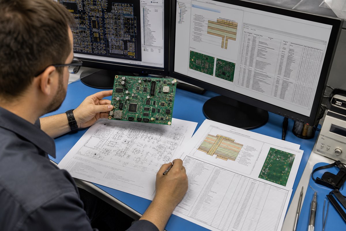
A medical device PCB design may work on the bench but still lose weeks in production because of mismatched revisions, unavailable parts, inaccessible test points, or unclear acceptance criteria.
Avoid those delays by releasing one buildable PCB/PCBA package before purchasing or tooling begins.
To simplify this handoff, EBest Circuit (Best Technology) gives you one sales contact backed by a three-person technical team for DFM, PCB fabrication, sourcing, assembly, inspection, and agreed testing.
What Medical Device PCB Design Must Define Before Manufacturing
Get an accurate quotation and prevent revision mistakes by sending one approved manufacturing package.
Include:
Gerber or approved ODB++/IPC-2581 data, drill files, and route data
fabrication drawing, stackup, impedance requirements, materials, finish, and tolerances
approved BOM with manufacturer part numbers and substitution rules
centroid data and assembly drawings with polarity, variants, and do-not-fit parts
programming, inspection, and test requirements with pass/fail criteria
one consistent revision across all files
If the fabrication drawing says revision B while the BOM says revision C, production should stop for clarification. Resolving that conflict before material purchase costs less than rebuilding an assembled batch.
EBest provides a DFM report showing the affected feature, manufacturing risk, recommended action, and required approval.
PCB Design Methods That Reduce Manufacturing Risk
Protect the next production lot by checking whether the layout fits a stable manufacturing and inspection process—not merely whether it passes CAD rules.
Before layout release, confirm:
trace, spacing, drill, annular ring, solder-mask, and copper-to-edge capability
stackup availability and controlled-impedance compatibility
component spacing, thermal pads, fiducials, tooling clearance, and depaneling method
access for AOI, X-ray, flying probe, ICT, or functional testing
whether HDI, via-in-pad, flex, or rigid-flex features are technically necessary
EBest’s experienced PCB/PCBA engineers identify process-fit problems before tooling, when changes cost less.
Material Selection for Reliable Medical PCBs
Avoid emergency substitutions by confirming material availability and approval rules before the build.
“FR-4” alone does not define laminate performance. Impedance, dimensional stability, assembly heat exposure, and future availability can depend on the exact laminate and construction.
Confirm in writing:
whether the exact laminate is mandatory or an approved equivalent is allowed
which dielectric values and thicknesses control impedance
operating conditions and assembly heat-cycle requirements
required material certificates, declarations, date codes, and lot records
who can approve a substitute and how approval will be recorded
EBest provides a BOM optimization list covering availability, lifecycle, package, and alternative-part risks before purchasing. EBest works with 1,000+ supply-chain partners; you retain approval of electrical equivalence and design changes.
How Medical Device PCB Assembly Changes the Design Review
Reduce handoff errors by reviewing the PCB, BOM, assembly data, and test requirements as one release.
Once components are added, the review must also cover land patterns, polarity, paste apertures, component height, moisture sensitivity, programming, inspection, and test limits.
EBest coordinates PCB fabrication, component sourcing, assembly, and agreed testing through one team.
A release-ready assembly package should define:
approved parts and substitution rules
polarity, variants, and do-not-fit components
solder alloy, paste, and relevant thermal constraints
programming files and verification requirements
inspection coverage and acceptance criteria
test method, fixture, software version, and pass/fail responsibility
EBest supports samples and small batches, helping you verify manufacturing, assembly, and testing before scaling.
When files, materials, test scope, and capacity permit, EBest can deliver PCBAs in approximately 1.5 weeks. Confirm the project-specific schedule in the quotation.
DFM Checks Before Prototype Release
Release prototypes with fewer open questions by requesting a DFM report that leads to decisions.
The review should cover:
stackup, thickness, copper weight, impedance, and drawing consistency
trace, spacing, drill, annular ring, mask dam, and edge clearance
via treatment, copper balance, panelization, tooling, and fiducials
footprint-to-BOM consistency, polarity, clearance, and paste apertures
test-point access and fixture constraints
revision alignment across every production file
Separate release blockers, customer approvals, and optional improvements affecting cost, yield, or lead time. Link every approved deviation to the applicable revision.
EBest’s experienced R&D and PCB/PCBA engineers provide practical process recommendations—not unexplained factory questions.
Inspection and Reliability Testing Evidence to Request
Make test results usable by defining what will be checked, against which limit, and what record you will receive. “100% tested” is not enough without a method and acceptance criteria.
Match each risk to evidence:
material identity: manufacturer, lot, date-code, and incoming records
bare-board opens and shorts: electrical or flying-probe results
placement and polarity: first-article and AOI records
controlled characteristics: specified impedance, microsection, cleanliness, or solderability reports
product function: customer-defined method, fixture, software, and pass/fail limits
investigation: serial number, work order, traveler, nonconformance, and corrective-action records
EBest’s ISO 13485:2016-certified quality system supports controlled revisions, suppliers, records, traceability, and nonconformances. ISO 9001, IATF 16949, and AS9100D qualifications are also listed. These certifications do not replace final device certification.
Our digital workshop can trace material and product batches, production cycles, and progress in as little as five seconds, according to company-provided capability data.
A Medical Device PCB Design Example for Release Control
Suppose a monitoring-board project is moving from successful samples to a 100-unit pilot build. The PCB files are revision B, the BOM is revision C, two parts have long lead times, one diode has no polarity note, and “functional test” has no limits.
Starting immediately risks assembling the wrong revision, using an unapproved substitute, placing the diode incorrectly, and producing test results that cannot be repeated.
A safer release path is:
Align all files under one approved revision.
Record the revision, polarity, and test gaps in the DFM report.
Provide BOM alternatives for customer approval before purchasing.
Confirm panel, assembly, inspection, and test responsibilities.
Build the pilot lot with the agreed production and traceability records.
Return build feedback before the next quantity increase.
Move from a working prototype to repeatable pilot production with approved files, parts, tests, and records.
What to Include in a Medical PCB Manufacturing RFQ
Compare suppliers on the same scope by sending a decision-ready RFQ.
Include:
prototype, pilot, and expected production quantities
one revision-aligned PCB/PCBA release package
material, stackup, finish, tolerance, workmanship, and panel requirements
sourcing, substitution, and consigned-material rules
programming, inspection, testing, documentation, and retention requirements
packaging, labeling, traceability, and target delivery date
Ask suppliers to list assumptions, open questions, material risks, tooling charges, and lead-time conditions. This makes quotations easier to compare.
EBest combines 20 years of PCBA experience with in-house PCB and PCBA factories. The company reports serving 10,000+ engineers and 1,800+ customers.
Send controlled files, quantities, and evidence requirements to sales@bestpcbs.com. Receive DFM questions, sourcing risks, process recommendations, and a project-specific delivery plan before release.
FAQs About Medical Device PCB Design
What should I receive from a DFM review?
A written report showing the affected feature, manufacturing risk, proposed action, and required approval.
How does ISO 13485 help a medical PCB/PCBA buyer?
It supports controlled processes, records, suppliers, traceability, and nonconformance handling. It does not certify the finished medical device.
When should BOM availability be reviewed?
Check critical parts before layout freeze and review the approved BOM again before material release.
Can EBest support prototypes before volume production?
Yes. EBest supports samples and small batches so engineers can validate manufacturing, assembly, inspection, and testing before scaling.
What should I send for an accurate medical PCBA quotation?
For an accurate medical device PCB design quotation, send aligned PCB and assembly files, the approved BOM, quantities, material requirements, substitution rules, inspection and test scope, traceability needs, and target delivery date to sales@bestpcbs.com.
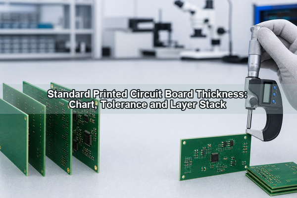
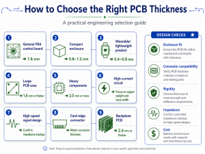
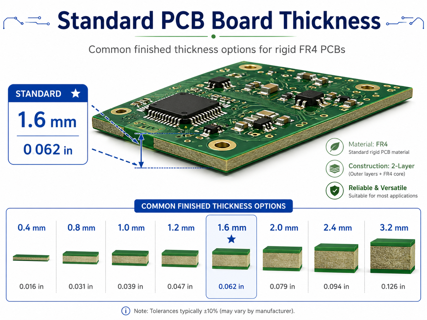
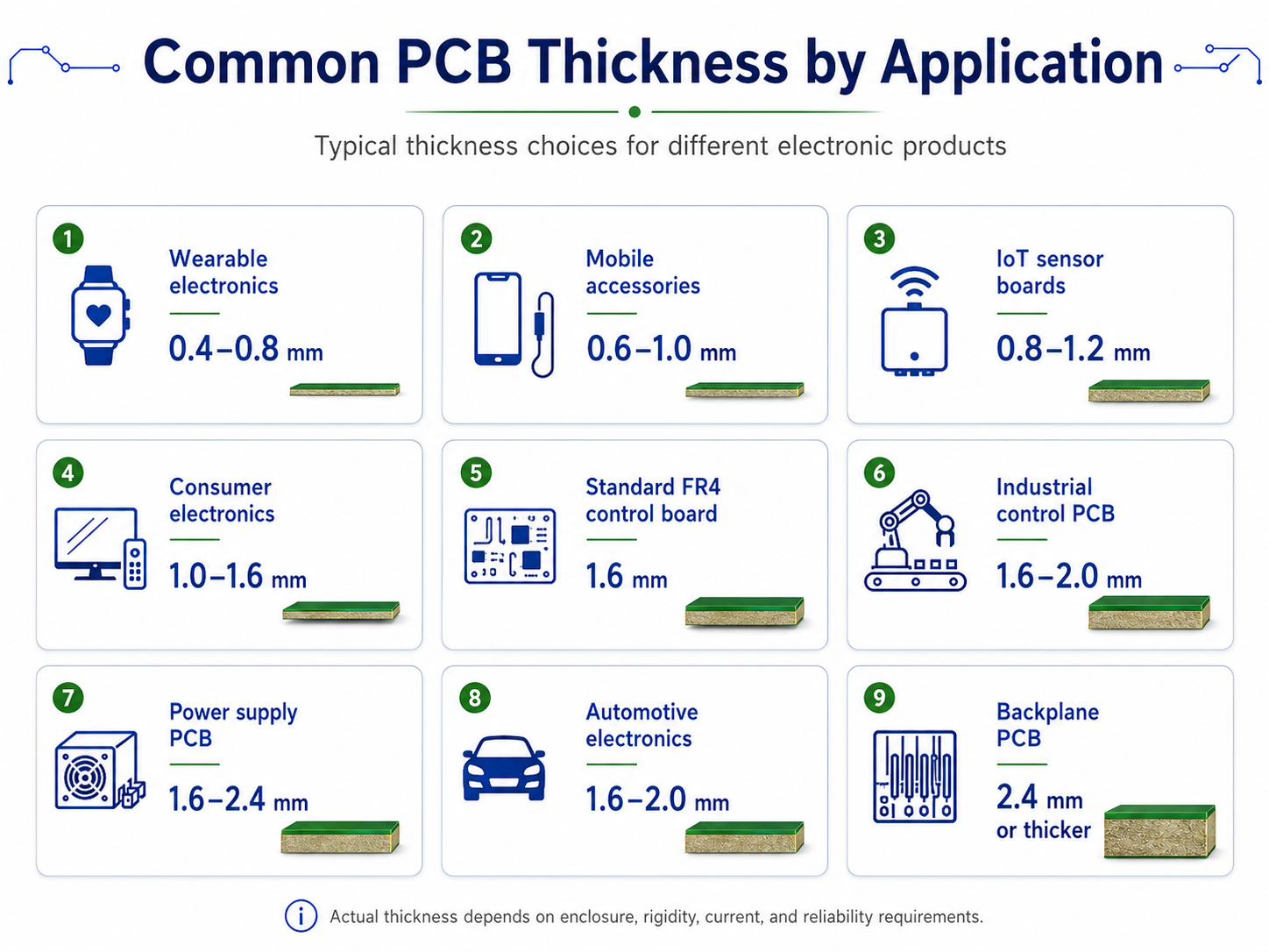
The most common standard printed circuit board thickness is 1.6 mm, approximately 0.062-0.063 inch or 62-63 mil. That value is a practical default for many rigid FR4 boards, but it is not a universal requirement. The correct finished thickness must also fit the layer stack, impedance geometry, connectors, enclosure, assembly process and mechanical load.
What Is the Standard Printed Circuit Board Thickness?
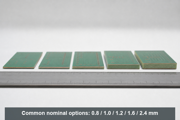
For a general-purpose rigid FR4 PCB, 1.6 mm is the conventional nominal finished thickness. The number developed from the older 1/16-inch laminate format, which equals 1.5875 mm. Modern fabrication drawings may state 1.57 mm, 1.60 mm, 0.062 inch or 0.063 inch, depending on the drawing convention and the fabricator’s standard material system.
“Standard” means commonly stocked and routinely processed, not mandatory. A compact sensor module can use 0.8 mm to reduce height. A card-edge board may need 1.6 mm to fit its connector. A large industrial board may use 2.0 mm or 2.4 mm for stiffness. The stated value should therefore be treated as the nominal finished board thickness, with a separate tolerance that defines the acceptable production range.
Standard PCB Thickness Chart in Millimeters, Inches and Mils
The chart below converts common rigid-board thickness options. Availability varies with laminate family, layer count, copper weight and the fabricator’s stocked constructions.
Nominal Thickness
Approx. Inches
Approx. Mils
Typical Design Direction
0.4 mm
0.016 in
16 mil
Very thin rigid modules and space-limited assemblies
0.6 mm
0.024 in
24 mil
Compact modules with controlled mechanical support
0.8 mm
0.031 in
31 mil
Thin consumer, handheld and daughterboard designs
1.0 mm
0.039 in
39 mil
Low-profile rigid boards with moderate stiffness
1.2 mm
0.047 in
47 mil
Space-saving multilayer and control boards
1.6 mm
0.063 in
63 mil
General rigid PCB default
2.0 mm
0.079 in
79 mil
Boards needing additional stiffness or stackup space
2.4 mm
0.094 in
94 mil
Industrial, connector or multilayer mechanical requirements
3.2 mm
0.126 in
126 mil
Thick rigid boards and demanding mechanical structures
These are nominal values rather than guaranteed measurements. The finished board is accepted against the thickness tolerance on the fabrication drawing. Conversion is also approximate because 1 mil equals 0.001 inch, while metric laminate systems are usually specified directly in millimeters.
Why Is 1.6 mm the Most Common PCB Thickness?
The 1.6 mm format remains common because material supply, fabrication tooling, connector geometry and product mechanics developed around the former 1/16-inch standard. It provides enough rigidity for many board sizes without making the assembly unnecessarily heavy. Fabricators can also build a wide range of 2-layer and multilayer constructions around this finished target.
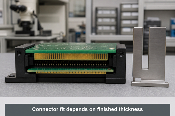
Component compatibility is another reason. Many card-edge connectors, board guides, standoffs and through-hole leads are designed around boards close to 1.6 mm. Using a thinner or thicker board can still be correct, but the mechanical interface must be checked rather than assumed. Press-fit hardware is especially sensitive because hole geometry, board thickness and pin engagement work together.
Cost is usually predictable at 1.6 mm because common cores and prepregs are readily available. A different thickness does not automatically make a PCB expensive, but a non-stock laminate construction, an unusual tolerance or a difficult multilayer build can require additional engineering and process control.
How Does PCB Thickness Differ From Copper Thickness?
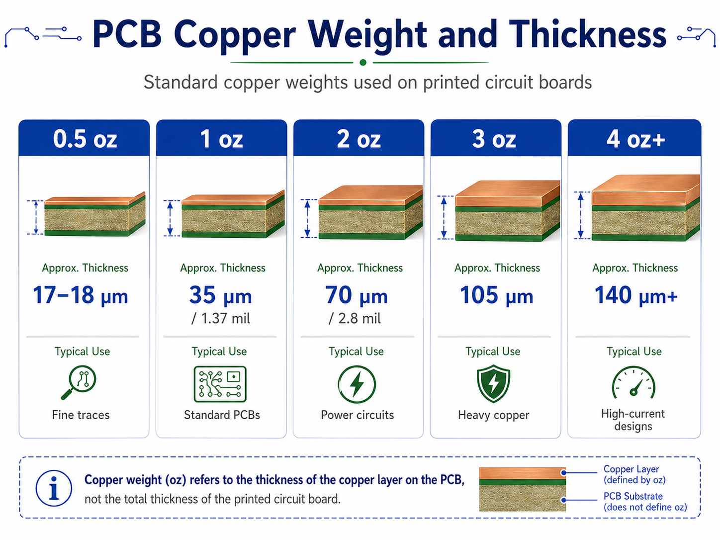
PCB thickness is the total finished board thickness. Copper thickness describes the conductor thickness on an individual layer. They are related in the stackup, but they are not interchangeable specifications.
Specification
What It Measures
Common Units
Main Design Effects
Finished board thickness
Total rigid PCB construction
mm, inch, mil
Mechanical fit, stiffness, stackup space and drilling aspect ratio
Copper thickness
Copper on one conductor layer
oz/ft², µm, mil
Current capacity, trace resistance, etching and spacing
Dielectric thickness
Insulation between selected copper layers
mm, µm, mil
Impedance, coupling, isolation and layer spacing
Typical nominal foil conversions are approximately 17 µm for 0.5 oz, 35 µm for 1 oz and 70 µm for 2 oz copper. Outer-layer finished copper may differ from starting foil because hole plating and pattern plating add copper. A 1.6 mm board can therefore use different copper weights without ceasing to be a 1.6 mm nominal board, provided the dielectric construction is adjusted accordingly.
A thick PCB is also not automatically a heavy-copper PCB. A 2.4 mm board with 1 oz copper is mechanically thick but does not use heavy copper. A 1.6 mm board with 4 oz copper is a heavy-copper design even though its total board thickness is conventional. The thick PCB board guide addresses the manufacturing effects of unusually thick rigid constructions.
What Determines Finished PCB Thickness?
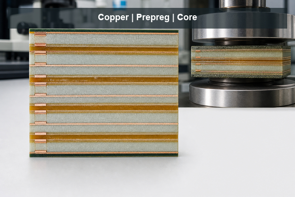
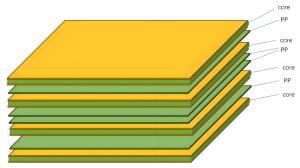
Finished thickness is created by the complete pressed stack, not by one laminate sheet. A 2-layer board may use a copper-clad core and solder mask. A multilayer board combines etched cores, prepreg bonding layers, outer copper, plating and surface coatings. Press temperature, pressure, resin flow and copper distribution affect the result.
Core thickness: defines much of the rigid dielectric structure and provides copper on one or both sides.
Prepreg type and count: determine bonding thickness after resin flows into copper features and cures.
Copper weight: changes the conductor height and the volume of resin needed to fill around traces and planes.
Layer count: adds copper and dielectric interfaces, increasing the number of variables in the pressed stack.
Plating and finish: add smaller local thickness contributions, especially on outer copper and hole walls.
Material system: affects resin content, glass style, pressed thickness, thermal expansion and availability.
Prepreg should not be treated as a fixed spacer before lamination. Its final thickness depends on glass style, resin content, copper pattern density and the press cycle. For controlled builds, the fabricator models the pressed result and selects a balanced set of cores and prepregs. A PCB thickness calculator can support an early estimate, but it cannot replace the production stackup.
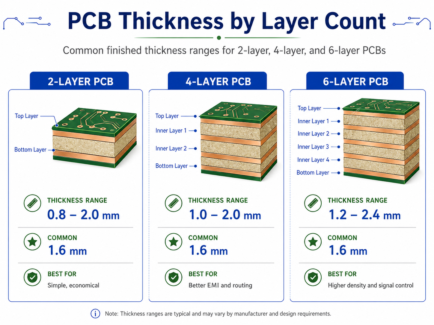
How Thick Are 2-, 4-, 6-, 8-, 12- and 32-Layer PCBs?
Layer count does not assign one compulsory board thickness. The finished value depends on routing density, copper weight, dielectric spacing, via structure and mechanical requirements. The following ranges are practical starting points for rigid FR4 discussions, not universal standards.
Layer Count
Common Starting Thicknesses
Important Constraint
2 layers
0.8, 1.0, 1.2 or 1.6 mm
Core thickness usually dominates the construction
4 layers
1.0, 1.2 or 1.6 mm
Plane spacing and outer copper affect the final build
6 layers
1.2, 1.6 or 2.0 mm
More dielectric interfaces must fit the impedance plan
8 layers
1.6, 2.0 or 2.4 mm
Routing density and via aspect ratio become more influential
12 layers
1.6, 2.0, 2.4 or 3.2 mm
Thin dielectrics or HDI may be needed to limit total thickness
32 layers
Custom multilayer construction
No universal value; lamination, drilling and reliability govern the build
A 4-layer PCB can be 0.8 mm or 2.0 mm, and a 12-layer PCB can sometimes remain near 1.6 mm by using thin cores and prepregs. That does not mean the thinnest possible build is best. Very thin dielectrics can increase coupling, demand tighter registration and make resin filling more difficult. Very thick builds can increase plated-hole aspect ratio and create longer via stubs.
The layer structure should be selected before the board outline and mechanical system are frozen. The related 4 layer vs 2 layer PCB comparison explains how the extra planes change routing and EMC behavior; thickness remains a separate, coordinated decision.
How Does PCB Thickness Affect Impedance and Signal Integrity?
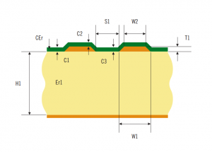
Total board thickness affects the available stackup space, but controlled impedance is governed by the local transmission-line geometry. Trace width, copper thickness, dielectric thickness, dielectric constant, solder mask and reference-plane relationship determine the impedance of a microstrip or stripline.
Changing a 1.6 mm board to 1.2 mm does not automatically change every trace impedance. If the relevant dielectric spacing and material properties remain the same, some signal layers may retain their geometry. In practice, however, reducing total thickness often forces changes to cores and prepregs, so the impedance model must be recalculated.
Thicker boards can also produce longer through-vias and longer unused via stubs. At higher data rates, those stubs may create resonances and insertion-loss problems. Backdrilling, blind vias or a different layer assignment may be needed. A production impedance control PCB therefore links the trace model to the confirmed laminate construction and measured impedance coupons.
How Does PCB Thickness Affect Mechanical Fit and Connector Compatibility?
Mechanical interfaces often set a harder thickness limit than the electrical circuit. Card-edge connectors specify an acceptable board-thickness range so their contacts apply the intended normal force. Board guides, slots, bezels, standoffs and enclosures also have limited clearance. A nominal change of a few tenths of a millimeter can affect insertion, alignment or screw loading.
Confirm card-edge connector slot width and contact engagement.
Check press-fit pin length, compliant-zone position and supported board range.
Verify standoff height, enclosure gaps and component clearance.
Review board span, mounting-hole spacing and bending load.
Include finished-thickness tolerance in the mechanical stack analysis.
Thin boards may need additional support during insertion or handling. Thick boards provide stiffness but increase weight and can move component terminals relative to the enclosure. The mechanical drawing should therefore use the full allowed thickness range, not only the nominal value.
How Does PCB Thickness Influence Warpage, Assembly and Reliability?
Board thickness contributes to bending stiffness, but warpage depends on material modulus, copper balance, stack symmetry, moisture, temperature and panel design. A thin board is more easily deflected by handling, component weight and reflow fixtures. A thick asymmetric board can still warp if copper and dielectric structures are poorly balanced.
During soldering, the PCB experiences a temperature gradient while copper, glass and resin expand at different rates. Large copper areas on one side, uneven component mass or an unbalanced stack can create bow and twist. The board warpage guide explains how stack symmetry, copper distribution, panel support and reflow conditions work together.
Assembly equipment also has practical limits. Very thin boards may require carriers for solder-paste printing, placement and reflow. Very thick boards have greater thermal mass and may need a profile that heats solder joints adequately without overstressing components. Depanelization, connector insertion and functional-test fixtures must use forces that do not bend or crack the finished assembly.
What Is PCB Thickness Tolerance and How Is It Measured?
PCB thickness tolerance is the permitted difference between nominal and actual finished thickness. A commercial rigid FR4 build commonly uses a percentage tolerance such as ±10%, but the actual requirement must be confirmed for the material, thickness and construction. A 1.6 mm board with ±10% tolerance has an acceptance range of 1.44-1.76 mm.
Tighter tolerance may be justified for card-edge contacts, press-fit components, controlled mechanical gaps or precision fixtures. It can require a more restricted material set and closer process control. The drawing should state the nominal value, tolerance and whether the measurement includes solder mask when that distinction is mechanically significant.
Finished boards are commonly checked with a calibrated micrometer or thickness gauge. Measurements should be taken at defined locations, away from edge burrs, local copper buildup or surface contamination. Multiple points reveal thickness variation across the panel. Cross-section analysis is used when the individual core, prepreg, copper or plating contributions must be verified rather than only the total board thickness.
When Should You Use a Thin or Thick PCB?
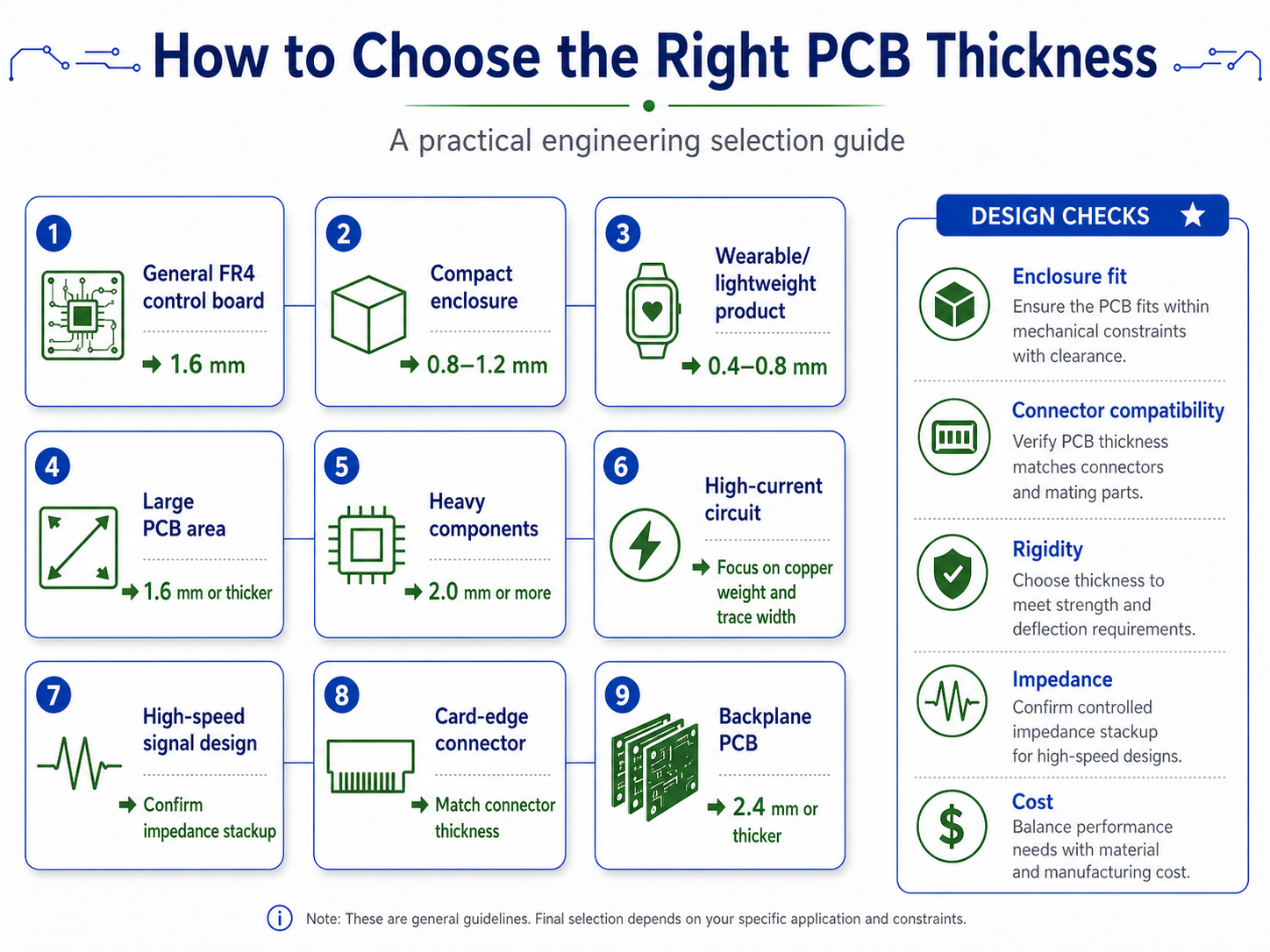
Use a thinner rigid PCB when product height and weight are constrained, the board is mechanically supported and the stackup can still meet impedance, insulation and assembly requirements. Common thin choices include 0.6, 0.8, 1.0 and 1.2 mm. An extra thin PCB needs more attention to handling, panel support, drilling and warpage than a conventional 1.6 mm board.
Use a thicker PCB when the structure needs greater stiffness, the layer stack needs more dielectric space, the board spans a large unsupported area or a connector system requires a specific engagement depth. Common thicker choices include 2.0, 2.4 and 3.2 mm. Thickness alone does not improve current capacity or thermal performance; copper geometry, material properties and the complete heat path still control those functions.
Keep 1.6 mm when it satisfies all electrical and mechanical constraints. It is usually the lowest-risk starting point because materials, assembly fixtures and connector ecosystems are widely compatible with it. Move away from that value only for a defined reason, then validate the linked stackup and mechanical changes.
How Should Finished Thickness Be Defined in PCB Documentation?
Gerber or ODB++ image data defines conductor, mask and legend geometry, but it does not reliably define the required finished board thickness. The value belongs in the fabrication drawing, manufacturing notes or an approved stackup table. The same controlled document should identify the unit and tolerance.
For a simple 2-layer board, a note such as “Finished board thickness: 1.60 mm ±10%” can be sufficient when no special stack construction is required. A controlled-impedance multilayer board needs an approved stackup showing layer order, copper weight, material family, core and prepreg construction, dielectric targets and finished thickness. Mechanically critical designs should also identify connector or press-fit constraints so the allowed range is consistent across drawings.
Revision control matters because changing finished thickness can alter enclosure fit, impedance geometry, via aspect ratio, test fixtures and assembly support. A thickness change should therefore trigger review of the stackup and mechanical interfaces instead of being treated as an isolated fabrication option.
FAQ About Standard Printed Circuit Board Thickness
Is 1.6 mm the only standard PCB thickness?
No. It is the most common rigid FR4 value, but 0.4, 0.6, 0.8, 1.0, 1.2, 2.0, 2.4 and 3.2 mm are also regularly used when the stackup and product mechanics support them.
How thick is a 2-layer PCB board?
A 2-layer rigid PCB is often 1.6 mm, but 0.8, 1.0 and 1.2 mm are common for compact products. The copper-clad core usually contributes most of the finished thickness.
How thick is a 4-layer PCB?
Many 4-layer PCBs use 1.6 mm, while 0.8, 1.0, 1.2 and 2.0 mm are possible. The selected cores and prepregs must provide the required plane spacing and impedance geometry.
Does a 12-layer PCB have to be thicker than 1.6 mm?
No. Some 12-layer constructions can fit within 1.6 mm by using thin dielectrics. Other designs need 2.0, 2.4 or 3.2 mm for routing, isolation, copper or via requirements.
Does thicker PCB material carry more current?
Not by itself. Current capacity depends mainly on copper thickness, trace or plane geometry, allowed temperature rise, airflow and the complete thermal path.
Can a PCB thickness calculator define the production stackup?
A calculator can estimate total thickness, but production values depend on pressed prepreg thickness, copper pattern, material data and lamination behavior. The fabricator’s confirmed stackup is the final reference.
Is solder mask included in finished PCB thickness?
Practices can differ. Solder mask contributes only a small amount, but mechanically critical drawings should state whether the specified finished thickness includes mask and where measurement is taken.
What tolerance is common for a 1.6 mm PCB?
±10% is a common commercial reference, corresponding to 1.44-1.76 mm, but the applicable tolerance depends on the material and construction and must be stated on the drawing.
Conclusion
Standard printed circuit board thickness is commonly 1.6 mm, but that default is only correct when the layer stack, impedance, connector, enclosure, assembly and tolerance requirements agree with it. A sound design separates total board thickness from copper thickness, defines the finished value in controlled documentation and verifies the actual production range.
EBest Circuit (Best Technology) manufactures rigid FR4 boards from very thin 2-layer constructions through thick multilayer builds, subject to material, stackup, dimensions and engineering review. For technical support on a thickness-sensitive PCB design, contact sales@bestpcbs.com.
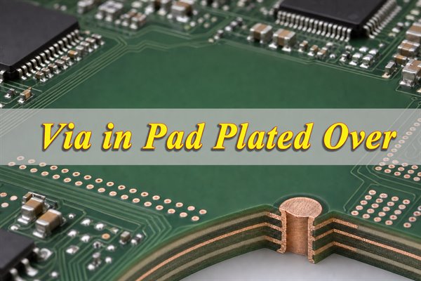
Via in pad plated over (VIPPO) places a filled, planarized and copper-capped via directly in a component land. It can free routing space under fine-pitch packages and create a solderable pad, but only when the fill, cap, surface flatness and fabrication notes are controlled as one manufacturing requirement.
The key question is whether the structure can be fabricated repeatedly without drawing solder from the joint or creating an uneven mounting surface. The quotation must cover filling, planarization, cap plating and inspection—not a vague request for “via in pad.”
What Is Via in Pad Plated Over (VIPPO)?
VIPPO is a complete via-protection structure, not simply a via located inside a pad. The hole is plated, filled, cured, planarized and plated over with copper so the finished land can receive solder paste and a component termination.
The barrel provides the electrical connection; the fill closes and supports the cavity. Planarization removes excess fill, and the copper cap restores a continuous solderable land. Without that closure, an open in-pad via can pull solder into the hole during reflow and contribute to solder starvation, component tilt or inconsistent joints.
How Does Via in Pad Plated Over Differ from Via-in-Pad and POFV?
Via-in-pad identifies where a via is placed; VIPPO and POFV identify how a filled via is finished. The terms overlap, but they are not interchangeable in every context. A via can sit inside a component pad without being filled or plated over, while a POFV structure does not have to be located in a component pad.
Terminology
Definition
Construction Requirements
Direct Component Soldering
Engineering Distinction
Via-in-Pad
Via location: the via is placed within a component land
May be open, tented, filled, covered or copper capped
Only when the selected treatment creates a flat, solderable land
It is a layout concept, not a complete fabrication specification. An open in-pad via can wick solder during reflow.
VIPPO
Via-in-pad plated over
The in-pad via is plated, filled, cured, planarized and copper capped
Yes, when the cap, flatness and final finish meet the approved requirements
VIPPO converts the in-pad via opening into a continuous component land and helps prevent solder loss into the hole.
POFV
Plated over filled via
The via is filled, planarized and plated over; its location depends on the design
Yes, if it forms an approved component land; otherwise it may serve another structural purpose
POFV is the broader process term. When the plated-over filled via is located inside a component pad, it is commonly treated as VIPPO.
Specify Via-in-Pad for placement, VIPPO when the via becomes part of a solderable component land, and POFV for the broader filled-and-plated-over process. VIPPO and POFV are commonly associated with IPC Type VII filled-and-capped via terminology, but the drawing must still identify the holes, fill, cap, surface finish, inspection criteria and applicable document revision.
When Should You Use VIPPO Instead of Dog-Bone Fanout?
Choose VIPPO only when it solves a verified routing, electrical, thermal or package-interface problem that dog-bone fanout cannot solve efficiently. Dog-bone fanout remains the lower-risk choice when an adjacent via and short surface trace fit within the routing rules and meet performance targets.
No escape space: Fine-pitch BGA, LGA and other dense bottom-terminated packages may leave no room for a trace neck and adjacent dog-bone via. Placing the via inside the land preserves the escape channel and can make inner pad rows routable.
Layer-count pressure: Direct vertical transitions can simplify breakout and may reduce escape layers or avoid extremely narrow traces and clearances. Compare the complete stackup cost because fewer layers may not offset the fill-and-cap process.
Short electrical path: Removing the dog-bone trace can reduce connection length, loop area and transition inductance for selected high-speed signals or power-decoupling paths. Confirm the benefit through channel or power-integrity analysis; a shorter visible trace does not guarantee better system performance.
Direct thermal path: A via array beneath a QFN, power device or exposed thermal pad can connect the land to internal planes or opposite-side copper. Evaluate via count, copper distribution, fill and stencil segmentation together to avoid paste loss or uneven package seating.
Solderable in-pad surface: Filling, planarization and copper capping restore a continuous pad for paste printing and component placement. An open, tented or resin-covered via is not equivalent when a component terminal sits over the opening.
Dog-bone fits: Keep the adjacent via when it meets routing and electrical requirements. It is easier to fabricate, inspect, probe and rework, and it separates via tolerances from the component land.
Prototype access: Debug builds benefit from accessible traces and test points. When density permits, dog-bone fanout makes trace cutting, pad repair and component rework easier.
Compare total cost rather than the via surcharge alone: VIPPO adds filling, curing, planarization, copper capping and inspection, while dog-bone routing may require more board area, finer lines or additional layers. Compare both complete constructions at prototype and production quantities using the same electrical and inspection requirements.
Confirm supply-chain capability before selecting VIPPO: The proposed via diameter, layer span, aspect ratio, fill material, cap structure, flatness and inspection plan must fit the fabricator’s qualified process. A layout is not ready simply because the CAD tool permits a via inside the pad.
Make the VIPPO vs. dog-bone fanout decision during DFM, not after routing is complete. Select VIPPO only when its routing or performance benefit outweighs the added fabrication, inspection and rework burden.
How Does the Via in Pad Plated Over Process Work?
Via in pad plated over is a controlled build-up process: form and plate the via, fill its cavity, cure and planarize the fill, then plate copper across the opening to restore a flat component land. The production route changes with through vias, blind vias, microvias, sequential lamination and the fabricator’s qualified process, but the functional stages remain similar. These dependencies become especially important in HDI PCB fabrication, where sequential lamination and stacked or staggered microvias must be reviewed as one construction.
Identify the designated vias: The fabrication data must show which holes require VIPPO, their finished size, layer span and associated component pads. This prevents ordinary vias from being filled unnecessarily and avoids ambiguity between through vias, blind vias and microvias.
Form the holes: Through and mechanically drilled blind vias are drilled with controlled tool size and registration; laser-drilled microvias are formed to the specified capture and target layers. Hole position and geometry must support reliable plating and later planarization.
Clean and prepare the hole walls: Debris and resin smear are removed, and the exposed dielectric is conditioned for metallization. Inadequate desmear can weaken the copper-to-dielectric interface or leave an unreliable electrical connection.
Metallize and copper-plate the barrel: A conductive seed layer is established before electrolytic copper builds the via wall. Barrel continuity and copper distribution must be acceptable before filling because the fill cannot repair thin plating, voids or poor interconnection.
Clean and fill the via: The cavity is prepared and filled with the approved conductive or non-conductive material under controlled pressure or vacuum. The process must limit trapped air, internal voids and incomplete fill, especially in small-diameter or high-aspect-ratio structures.
Cure the fill material: The filled panel follows the material supplier’s qualified time-and-temperature profile. Complete cure stabilizes the plug for planarization and later thermal cycles; under-cure can cause recession, cracking, contamination or cap-plating defects.
Planarize the surface: Excess fill is removed until the plugged via is level with the surrounding copper land. The operation must avoid a recessed plug, a raised bump, excessive copper removal or damage to nearby fine features because these conditions can affect solder-paste deposition and component coplanarity.
Deposit and plate the copper cap: The planarized opening is prepared, metallized and copper plated to create a continuous land over the filled via. Cap adhesion, coverage and thickness must meet the drawing and applicable acceptance criteria; filling alone does not create a VIPPO soldering surface.
Complete the outer-layer features and finish: Imaging and etching define the final pad, after which solder mask and the specified surface finish are applied. The finished land must remain compatible with the selected BGA, QFN, LGA or other bottom-terminated component assembly process.
Inspect and release the structure: Visual and dimensional checks assess pad flatness, surface defects and registration, while microsection or other agreed methods evaluate barrel copper, fill condition, cap continuity and internal interfaces. Sampling, acceptance limits and reporting should be defined before production rather than after a defect occurs.
A sound copper cap cannot compensate for poor hole-wall plating, trapped voids, incomplete cure or excessive planarization. Each stage must pass its own process control before the next operation begins.
Should VIPPO Vias Use Conductive or Non-Conductive Fill?
Non-conductive epoxy is a common choice because the plated barrel and copper cap carry the electrical current. Conductive fill may be considered for a specific thermal or electrical objective, but it should not be specified automatically.
Decision factor
Non-conductive fill
Conductive fill
Electrical path
Current remains in the plated barrel and cap
Fill may contribute, but performance depends on material and interfaces
Thermal objective
Suitable when the copper structure provides the required path
Consider only when thermal analysis supports the benefit
Process control
Well suited to filling and planarization when matched to the via geometry
Material handling, cure behavior and plating compatibility require confirmation
Cost
Usually the more economical option
Typically carries a material and process premium
The broader PCB via filling decision must also account for board thickness, finished via diameter, aspect ratio, via span, pad construction and reliability target. Approve the fill only after those variables have been reviewed; a material label alone is not a complete specification.
What Via in Pad Plated Over Design Rules Must Be Confirmed Before Layout Release?
The critical VIPPO PCB design rules must be agreed with the fabricator before the footprint and fanout are frozen. Generic capability values may not apply to the selected layer span, laminate, copper weight, via type or reliability class.
Via type and layer span: Identify whether each feature is a through via, mechanically drilled blind or buried via, or laser-drilled microvia, and state its start and stop layers. These structures use different formation, plating and filling routes, so one rule cannot be applied to all of them.
Drill size and finished hole size: Distinguish the tool or laser diameter from the finished plated opening. Confirm the tolerance and whether the drawing refers to the drilled, plated or final filled condition; mixing these definitions can invalidate aspect-ratio and plating reviews.
Pad, capture land and annular ring: Check the component manufacturer’s land pattern, drill-to-pad registration allowance, required annular ring and area available for the copper cap. The design must retain a usable solderable land after fabrication tolerances, planarization and etching are considered.
Aspect ratio and plating access: Review hole depth relative to diameter for each via family and confirm that chemistry can circulate through the structure. Deep or narrow vias are harder to metallize and fill consistently; blind, buried and through vias should therefore be reviewed separately.
Microvia stacking and staggering: Define whether microvias are staggered, stacked or placed over a buried via, and confirm the permitted build-up sequence. Stacked structures concentrate stress and depend on the underlying fill and cap, so they may require additional process qualification and inspection.
Fill material and filling scope: Specify conductive or non-conductive fill only when the electrical or thermal design requires it, and identify exactly which vias are included. Also confirm material compatibility with lamination, cure temperature, surface finish and assembly thermal cycles.
Copper cap and surface condition: Define which side or sides require plating over, the required cap construction and the acceptance basis for continuity, adhesion and surface condition. Filling and tenting alone do not create a flat, solderable VIPPO land.
Pad flatness and finished height: Agree how recess, protrusion and coplanarity will be measured and accepted. A recessed pad can disturb paste transfer, while a raised pad can prevent a BGA, LGA or QFN from seating evenly on adjacent lands.
Solder mask and surface finish: Coordinate solder-mask-defined or non-solder-mask-defined lands, mask clearance and final finish with the footprint and assembly process. Confirm that mask registration and finish thickness will not reduce the intended solderable area or create uneven pad height.
Electrical, thermal and assembly performance: Include high-speed via transitions and stubs in the channel model, and evaluate the complete copper-and-dielectric heat path for thermal pads. Then review stencil aperture, paste volume, package warpage, component coplanarity and reflow profile; conductive fill should not be treated as an automatic solution to signal, heat or solder-joint problems.
Do not release the layout until the fabricator has reviewed the proposed stackup, via table and representative component escape. Record the approved values in the controlled fabrication drawing or design rules rather than leaving them in email. Any change to laminate, copper weight, layer span, via diameter, fill system, surface finish or component footprint should trigger a focused VIPPO review before the data is released again.
How Should VIPPO Be Called Out in the Fabrication Drawing and Data Package?
A complete VIPPO callout identifies exactly which vias are filled and capped and how acceptance will be determined. A note that says only “plug vias” is open to interpretation.
Dedicated identification: Provide a separate drill layer, via table or unambiguous coordinate-based designation for VIPPO holes.
Structure definition: State the via span, whether it is through, blind, buried or microvia, and which surface receives the cap.
Material requirement: Specify conductive or non-conductive fill, or authorize the fabricator to propose a qualified material for approval.
Process requirement: Require filling, curing, planarization and copper capping where a solderable land is needed.
Acceptance basis: Cite the applicable drawing, IPC product class, standard revision and any project-specific microsection or surface criteria.
Data consistency: Ensure Gerber/ODB++, NC drill, stackup, drawing and netlist describe the same revision.
A practical note may state: “Fill designated vias with approved non-conductive epoxy, cure, planarize and copper cap to form solderable lands; use IPC-4761 Type VII terminology where invoked; acceptance per the approved drawing and applicable product specification.” Add project-specific values only after engineering agreement.
What VIPPO Defects Cause Fill Voids, Surface Depressions or Soldering Problems?
Most VIPPO failures begin with incomplete filling, poor planarization, weak cap plating or an already-defective plated barrel. The visible soldering symptom may appear late even though the cause was introduced during bare-board fabrication.
Fill voids: Trapped air, poor fill penetration or unsuitable geometry can leave cavities that reduce support and may affect later thermal cycling.
Surface depression: Fill shrinkage or underfilling can leave a recessed pad that changes paste distribution and joint geometry.
Raised surface: Excess fill or insufficient planarization can prevent a package from seating evenly.
Cap discontinuity: Thin, porous or cracked cap copper can expose the fill or create a weak solderable surface.
Barrel defect: Smear, plating voids or cracks remain electrical and reliability risks even when the top cap looks acceptable.
Moisture or contamination: Inadequate cleaning, cure or storage control can contribute to blistering, delamination or assembly defects.
Solder wicking should trigger an investigation of the actual via construction and cap integrity; it is not normal behavior for a correctly produced VIPPO structure.
How Should Finished Via in Pad Plated Over Vias Be Inspected and Accepted?
A complete via in pad plated over inspection plan combines surface inspection, dimensional checks, representative microsections and bare-board electrical testing. No single method verifies the soldering surface, copper cap, cured fill, plated barrel and electrical network.
Confirm the acceptance basis: Before inspection, verify the released fabrication drawing, product class, applicable IPC document and revision, approved stackup, via map and any customer-specific requirements. The purchase package should define what is measured, the sampling plan, acceptance limits and required records; otherwise the supplier and customer may judge the same feature differently.
Inspect the finished pad surface: Use appropriate lighting and magnification to check that the component land is continuous and clean. Reject or escalate exposed fill, open cap areas, pits, nodules, dents, scratches, contamination, lifted copper or damage that could interfere with solder-paste printing, wetting or component seating.
Verify pad flatness and coplanarity: Measure the features specified on the drawing rather than relying on visual appearance. A recessed plug can reduce paste support, while a raised cap can hold a BGA, LGA or QFN terminal above adjacent lands. Measurement method, datum, sample quantity and allowable variation should be agreed before production.
Check registration and finished geometry: Confirm that the plated-over area remains correctly located within the component land and that the final pad dimensions support the approved footprint. Misregistration, excessive planarization or over-etching can reduce the usable solderable area even when the via is electrically continuous.
Review the copper cap: Cross-sectional evidence should show a continuous plated cap with no separation from the surrounding copper. Assess the cap thickness and coverage against the drawing and applicable acceptance criteria. A filled via without an acceptable copper cap is not an acceptable VIPPO soldering land.
Evaluate the fill condition: On representative coupons or agreed production samples, examine fill completeness, internal voiding, recession, cracks and separation at the fill-to-barrel or fill-to-cap interfaces. The permitted condition must come from the governing specification and customer agreement because a generic void percentage does not describe every via geometry or reliability requirement.
Examine the plated barrel and interconnect: Microsections should also assess hole-wall copper, internal-layer connections, corner condition and evidence of plating voids, cracks or separation. Good fill appearance cannot compensate for a weak conductive barrel or an unreliable connection to the target layer.
Perform bare-board electrical testing: Test continuity and isolation using the approved netlist and test method. Electrical testing identifies opens, shorts and incorrect connectivity, but it cannot confirm pad flatness, cap adhesion, fill cure or all internal structural defects, so it must support rather than replace physical inspection.
Use assembly validation when risk justifies it: For a new fine-pitch footprint, new VIPPO construction or high-reliability program, inspect first-article paste deposits, component seating and solder-joint consistency. X-ray or other assembly inspection may reveal solder loss, voiding or alignment problems, but the method and acceptance criteria should match the package and product requirements.
Review lot records before release: Confirm the required certificate, electrical-test result, microsection images, dimensional report, material traceability and nonconformance history. Any out-of-limit result should be documented and dispositioned through the agreed deviation or corrective-action process, not accepted through an undocumented production judgment.
“Inspect to IPC” is not a complete acceptance instruction. The order should identify the document and revision, product class, designated VIPPO structures, cap and fill requirements, dimensional controls, sampling, records and rules for reporting nonconforming results.
How Does VIPPO Affect PCB Cost, Yield and Lead Time?
Via in pad plated over costs more than an open or simply covered via because it adds controlled operations and yield exposure. The premium depends on the number and geometry of filled vias, panel construction, material, inspection plan and production volume.
Cost drivers include selective or full-panel filling, cure cycles, planarization, additional copper processing, microsections and yield loss when flatness or fill quality fails. Conductive fill normally adds further material and qualification cost.
VIPPO can extend lead time because filling, curing, planarization, cap plating and, when required, microsection review are sequential operations. Material approval, unclear via classifications, or failed fill and flatness checks can add engineering holds, reprocessing or remake time. Confirm the approved construction and inspection plan before order release to reduce avoidable schedule delays.
Compare quotations against the same technical package. A low quote may exclude cap plating, treat VIPPO as ordinary plugged vias or omit required quality records.
What Should You Send for a VIPPO DFM Review and Quote?
Send one revision-controlled package that connects the component land, via structure, stackup, fabrication note and acceptance requirement. This allows engineering to review manufacturability before pricing is finalized.
PCB production data: Gerber or ODB++, NC drill files, netlist and a clear revision identifier.
VIPPO map: Designated via locations, via span, finished hole requirement, fill choice and cap side.
Fabrication drawing: Applicable standard, product class, surface finish, inspection criteria and required quality records.
Assembly context: BOM, assembly drawing, centroid data and relevant BGA/QFN package information when assembly is included.
Commercial inputs: Prototype and production quantities, delivery target and expected approval stages.
EBest Circuit will confirm final VIPPO capability against the submitted stackup and via construction. Do not release the layout based on a generic capability value.
FAQs About Via in Pad Plated Over
Q1: Is an open via-in-pad acceptable for a hand-soldered prototype?
A1: It may be workable only when the joint is visible and additional solder can be applied. The result is process-dependent. For hidden BGA joints, fine-pitch parts or a design intended for production reflow, do not use hand-solder success as proof of production reliability.
Q2: Can I plug a via with solder or epoxy myself instead of ordering VIPPO?
A2: A manual plug may help a one-off experiment, but it is not equivalent to production VIPPO. It does not reproduce controlled hole filling, cure, planarization and copper capping and may trap flux or air, remain uneven or remelt during assembly. Therefore, do not treat it as a production substitute.
Q3: Does VIPPO make BGA or small-component rework more difficult?
A3: Yes, VIPPO can make component rework more difficult. The short direct connection to internal copper may increase local heat demand, and a pad integrated with a via is harder to isolate or repair if damaged. Establish the rework profile, board support and inspection method before attempting high-value BGA removal or replacement.
Q4: Can a VIPPO land replace a dedicated test point?
A4: No—do not assume a VIPPO land can replace a dedicated test point. A land under a component is inaccessible after assembly, while an exposed plated-over via may not have the probe area, spacing or durability needed for repeated contact. Preserve dedicated test access for programming, ICT and troubleshooting unless the test engineer approves another method.
Q5: Can VIPPO under one pad of a small passive cause tombstoning?
A5: Yes, tombstoning can still occur despite using VIPPO. VIPPO prevents an open hole from draining solder, but the two terminations may still heat or wet unevenly. Compare copper balance, plane connections, paste volume and pad geometry on both ends because a capped via does not eliminate thermal imbalance.
Q6: Will VIPPO stop potting compound or conformal coating from passing through a via?
A6: A properly filled and copper-capped via closes that specific leakage path. Coating or potting qualification must still consider board edges, connectors, other holes, material adhesion and thermal expansion because VIPPO addresses only the designated via opening.
Q7: Does VIPPO eliminate the need for X-ray inspection under a BGA?
A7: No, VIPPO does not eliminate the need for BGA X-ray inspection. It removes the open via cavity from the land, but hidden solder joints can still have insufficient solder, bridging, voiding or alignment defects. Use an inspection plan matched to the package, process risk and acceptance requirements.
Q8: Can a defective VIPPO copper cap be repaired after final surface finishing?
A8: A defective copper cap should not be repaired without formal engineering approval. Local rework may not restore the original cap interface, flatness, finish or reliability. Do not accept a cosmetic touch-up as an equivalent repair without an approved procedure and inspection evidence.
Q9: Can components be mounted on opposite sides over the same filled and plated via?
A9: Double-sided component placement may be feasible when both surfaces are intentionally capped. The nets, pad geometries and assembly sequence must also be compatible. Confirm side-specific flatness, finish, paste printing and reflow constraints because double-sided placement is both a fabrication and assembly decision.
Q10: Should a prototype and its production version use the same via treatment?
A10: Use the production VIPPO construction when the prototype must validate assembly yield or reliability. A simplified open or tented via may reduce prototype cost, but it changes paste behavior and can hide production risks. Document every prototype deviation before interpreting the results.
Send your design for a VIPPO DFM review before order release. Email the Gerber or ODB++ files, stackup, via table, BOM, quantities and assembly requirements to sales@bestpcbs.com. Include the delivery target and any impedance, surface-finish, inspection, programming or functional-test requirements. We will review the via construction, identify manufacturing risks and prepare a production quotation.
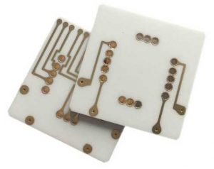
ceramic pcb prototype production is the controlled sample-building stage used to verify a ceramic circuit design before volume manufacturing. It helps engineers confirm substrate choice, copper pattern, thermal path, tolerances, assembly risk, and test requirements before committing to production tooling or a larger order.
For buyers and hardware teams, a ceramic PCB prototype is not just a small quantity of boards. It is a practical engineering checkpoint for high-power LEDs, power modules, sensors, RF designs, automotive electronics, medical devices, and other circuits where heat, dimensional stability, insulation, or reliability can decide whether the final product works.
What Is Ceramic PCB Prototype Production?
Ceramic PCB prototype production is the first manufacturing run of a ceramic circuit board design, usually built to validate the material, copper layout, process route, inspection plan, and assembly compatibility. The goal is to find manufacturability issues while the design can still be corrected without large production losses.
Unlike a standard FR4 prototype, a ceramic prototype depends heavily on substrate behavior, metallization method, firing or bonding process, conductor adhesion, surface flatness, and thermal expansion matching. A good prototype order should therefore answer both electrical and manufacturing questions, not only confirm that the Gerber files can be plotted.
For a new project, the prototype stage often confirms whether ceramic PCB technology is the right direction, or whether an alternative such as FR4 PCB or metal-core PCB is enough for the thermal and cost target.
Why Is Ceramic PCB Prototyping Different from FR4 PCB Prototyping?
Ceramic PCB prototyping is different because the substrate is rigid, hard, thermally conductive, and much less forgiving than glass-reinforced epoxy laminate. The process needs more attention to ceramic material selection, copper bonding, drilling or laser processing, dimensional tolerance, and thermal cycling behavior.
Prototype factor
FR4 PCB prototype
Ceramic PCB prototype
Base material
Glass epoxy laminate
Al2O3, AlN, BeO alternatives, LTCC, HTCC, or other ceramic substrates
Main design concern
Signal routing, layer stack, cost, and standard fabrication limits
Thermal path, ceramic thickness, copper adhesion, CTE match, and process route
Mechanical behavior
Can flex slightly before fracture
Brittle and requires careful handling, panel design, and fixture planning
Prototype review focus
DFM, impedance, hole quality, solder mask, assembly fit
Metallization quality, substrate flatness, thermal design, edge quality, and inspection plan
This difference affects the RFQ stage. A supplier should review not only the Gerber data, but also the ceramic material, copper thickness, board outline, via structure, tolerance needs, component heat load, and whether the prototype must support later mass production approval.
Which Ceramic PCB Material Should You Choose for a Prototype?
The best ceramic prototype material depends on thermal conductivity, insulation requirement, mechanical strength, cost target, and the final application environment. Al2O3 is commonly chosen for cost-effective ceramic prototypes, while AlN is often selected when higher thermal conductivity is required.
Material or technology
Why it is used in prototypes
Typical review point
Al2O3 ceramic
Balanced cost, insulation, mechanical stability, and mature processing
Check whether thermal performance is enough for the heat load
AlN ceramic
Higher thermal conductivity for power and LED designs
Confirm cost, availability, and metallization compatibility
Thick film ceramic
Useful for printed conductor, resistor, and hybrid circuit structures
Review conductor geometry and fired pattern tolerance
Thin film ceramic
Used where fine lines, stable circuits, or precise patterns are needed
Confirm line width, adhesion, finish, and application fit
DPC, DCB, or related structures
Selected when copper thickness, thermal path, or power handling drives the design
Match the process route to copper thickness and reliability needs
If the project is still early, ask the manufacturer to compare available ceramic options before confirming the prototype route. EBest Circuit supports ceramic PCB categories such as thick film ceramic PCB, thin film ceramic PCB, DPC ceramic PCB, and DCB ceramic PCB, so the prototype can be planned around the final production requirement instead of treated as an isolated sample.
What Is the Ceramic PCB Manufacturing Process?
The ceramic PCB manufacturing process usually starts with design review and material selection, then moves through substrate preparation, metallization, patterning, firing or bonding, surface finish, profiling, inspection, testing, and packing. The exact route depends on whether the project uses thick film, thin film, DPC, DCB, LTCC, HTCC, or another ceramic process.
Material preparation: Select Al2O3, AlN, or another ceramic substrate and confirm thickness, size, flatness, and handling needs.
Metallization and patterning: Build the conductive layer using the selected process route, then define circuit features according to the design.
Thermal or bonding process: Fire, sinter, plate, bond, or otherwise stabilize the conductor system depending on the technology.
Finishing and profiling: Apply the required surface finish, cut the outline, and prepare the board for inspection or assembly.
Inspection and test: Review dimensions, conductor quality, insulation, open/short status, surface quality, and packaging condition.
A prototype should be reviewed as a process sample. If the prototype later moves into production, the same data package, material choice, and inspection criteria should be stable enough to repeat.
How Do Thick Film, Thin Film, DPC and DCB Affect Prototype Production?
Different ceramic PCB process routes affect prototype cost, minimum features, copper thickness, thermal performance, and sample lead time. Choosing the process too late can force the engineering team to redesign pads, traces, vias, or thermal areas after the first prototype.
Thick film ceramic PCB is often used for hybrid circuits and printed conductor structures. It can be practical for prototypes where fired pastes, resistive elements, or ceramic-based circuit patterns are part of the design.
Thin film ceramic PCB is better suited for finer features and stable circuit requirements. It is often reviewed for sensor, microwave, medical, and precision electronic applications where conductor geometry matters.
DPC and DCB ceramic PCB routes are more closely tied to power electronics and heat transfer. For these prototypes, copper thickness, adhesion, thermal cycling, and substrate-to-copper reliability need early review.
What Files Are Needed for a Ceramic PCB Prototype Quote?
A ceramic PCB prototype quote is more accurate when the supplier receives a complete technical package, not just a screenshot or partial Gerber export. Missing tolerances, material notes, and assembly requirements can cause delays or a quote that does not match the real production risk.
Gerber files and drill data
Board outline drawing with critical dimensions
Ceramic material preference, such as Al2O3 or AlN
Substrate thickness and copper thickness requirement
Surface finish requirement
Panelization or single-piece delivery preference
Quantity for prototype and expected production volume
Assembly files if the prototype needs PCBA service
Thermal, electrical, or reliability test requirements
Application notes, especially for high-power, high-temperature, LED, sensor, or RF use
When a buyer provides both the prototype quantity and the expected mass production target, the manufacturer can recommend a route that avoids sample-only shortcuts that may not scale.
What Should You Check Before Moving from Prototype to Production?
Before moving from ceramic prototype to production, check whether the prototype truly validates the final design, process, material, and inspection standard. A board that passes a simple electrical test may still need thermal, mechanical, and assembly review before mass production.
Confirm the ceramic material and thickness match the final thermal design.
Check conductor adhesion, line quality, edge quality, and surface finish.
Review substrate flatness and dimensional tolerance against assembly needs.
Test open/short status, insulation resistance, and critical electrical paths.
Review solderability or bonding compatibility if components will be mounted.
Record any design changes before approving the production file set.
Ask whether the same process route will be used for the production batch.
The cleanest transition happens when the prototype report, customer feedback, corrected files, and final production requirements are all connected before the next purchase order.
What Problems Can Delay Ceramic PCB Prototype Production?
Ceramic PCB prototype production is often delayed by incomplete files, unclear material selection, unrealistic tolerances, process-route mismatch, missing assembly data, or late changes to the thermal design. These problems are easier to fix before production starts than after substrates and tooling have been prepared.
Delay cause
Why it matters
How to prevent it
Unclear ceramic material
Al2O3, AlN, and other ceramics change cost and thermal behavior
Share heat load, application, and target cost before quoting
Missing tolerance drawing
Ceramic processing may need different tolerance planning than FR4
Mark critical dimensions and non-critical dimensions separately
Wrong process route
Thick film, thin film, DPC, and DCB do not fit the same designs equally
Ask the supplier to review process fit before sample build
Late assembly requirement
Pad finish, flatness, and component heat transfer may need early planning
Send BOM, placement file, and assembly notes with the RFQ
How to Choose a Ceramic PCB Prototype Manufacturer?
Choose a ceramic PCB prototype manufacturer by checking whether the supplier can review material selection, process route, DFM risk, inspection requirements, assembly needs, and future production scaling. Price matters, but the cheapest sample is not useful if the process cannot support the final product.
Good supplier questions include:
Which ceramic materials and process routes are suitable for this design?
Can the same route support prototype and mass production?
What design features may increase cost or delay?
Which tolerances should be relaxed if they are not functional?
What tests are recommended for this application?
Can assembly, inspection, and packaging be coordinated in one project flow?
EBest Circuit can support custom ceramic PCB projects from prototype review to sample production and later batch manufacturing. For projects that need assembled samples, prototype PCB fabrication can also be coordinated with PCBA review to reduce handoff risk.
FAQ
How much does a ceramic PCB prototype cost?
Ceramic PCB prototype cost depends on material, substrate thickness, copper thickness, process route, dimensions, tolerance level, quantity, surface finish, testing, and whether assembly is included. Al2O3 prototypes are often more cost-effective than higher thermal conductivity ceramic options, but the right choice should be based on the heat load and reliability target.
Can ceramic PCB prototypes be assembled?
Yes, ceramic PCB prototypes can be assembled when the pad finish, flatness, component package, soldering or bonding method, and thermal requirements are reviewed early. If assembly is needed, send the BOM, placement file, polarity notes, and any thermal interface requirements with the PCB quotation package.
Is Al2O3 or AlN better for ceramic PCB prototype production?
Al2O3 is often selected for balanced cost and mature processing, while AlN is chosen when higher thermal conductivity is required. The better option depends on the heat source, insulation requirement, mechanical design, available budget, and whether the prototype must represent a later production build.
Can one ceramic PCB prototype be used for mass production approval?
One prototype can support production approval only if it uses the same material, process route, design file set, tolerance standard, inspection method, and assembly assumptions planned for mass production. If the prototype used sample-only changes, a second verification run may be needed before release.
What tolerances matter most in ceramic PCB prototyping?
The most important tolerances are usually board outline, hole or slot position, substrate thickness, copper feature size, registration, flatness, and critical pad locations. The buyer should identify which dimensions affect assembly or function, because unnecessary tight tolerances can increase cost and delay without improving performance.
What is the difference between ceramic prototype and ceramic PCB prototype?
A ceramic prototype can refer to any trial part made from ceramic material, while a ceramic PCB prototype is a circuit board sample built on a ceramic substrate with conductive patterns for electronic use. For RFQ clarity, use ceramic PCB prototype when the part includes circuit fabrication requirements.
How Can EBest Circuit Support Ceramic PCB Prototype Production?
EBest Circuit supports ceramic PCB prototype production by helping buyers review materials, process route, manufacturability, inspection needs, and assembly requirements before moving into larger production. If you are developing a ceramic PCB for LED, power electronics, sensor, automotive, medical, or industrial electronics applications, send your files and requirements to the engineering team for a practical review and quotation at sales@bestpcbs.com.
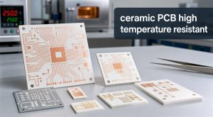
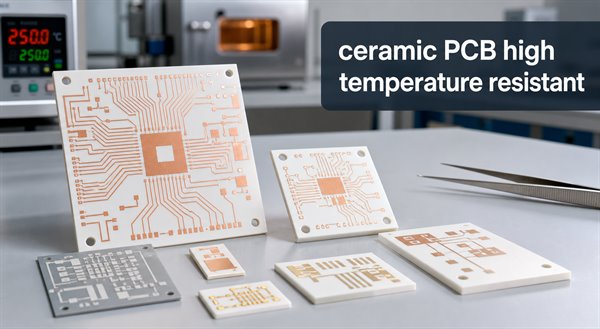
A ceramic PCB can be a strong choice for high temperature electronics when FR4, standard metal core PCB, or ordinary laminate materials cannot provide enough temperature stability, insulation, or heat transfer. The right material still depends on actual operating temperature, heat load, thermal cycling, CTE matching, copper structure, assembly method, and inspection requirements.
What Does Ceramic PCB High Temperature Resistant Mean?
Ceramic PCB high temperature resistant means the circuit substrate can keep useful electrical insulation, dimensional stability, and mechanical integrity in a hotter environment than many organic PCB materials can tolerate.
For PCB buyers, high temperature resistance should not be read as one simple number. A board may survive a short thermal event but still fail in long-term operation because of copper stress, solder joint fatigue, ceramic cracking, metallization adhesion, component limits, or repeated thermal cycling.
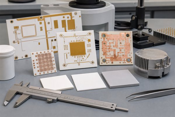
A ceramic PCB is usually chosen when the substrate must support both heat transfer and electrical reliability. Alumina, aluminum nitride, silicon nitride, thick film ceramic circuits, DBC ceramic PCB, and other ceramic substrate options each solve a different high temperature problem.
Why Choose Ceramic PCB for High Temperature Applications?
Choose ceramic PCB for high temperature applications when the board must handle heat, insulation, and dimensional stability at the same time.
Standard FR4 PCB works well for many electronic products, but its resin system limits long-term high temperature reliability. High Tg FR4 can improve heat resistance, yet it is still an organic laminate. Ceramic substrates are inorganic, so they can offer stronger temperature stability and lower thermal expansion in harsh environments.
Common high temperature ceramic PCB applications include LED modules, power electronics, semiconductor modules, automotive electronics, industrial sensors, heating control circuits, aerospace electronics, high-voltage insulation circuits, and compact assemblies where heat cannot be removed easily through a standard board stack.
PCB Option
High Temperature Fit
Buyer Note
FR4 PCB
Good for many standard products
Check Tg, Td, operating temperature, and soldering profile
High Tg FR4
Better than standard FR4
Useful when temperature is elevated but not extreme
Often used for LEDs and power boards, but dielectric layer matters
Ceramic PCB
Strong heat resistance and insulation
Best when heat, voltage, reliability, and size all matter
DBC ceramic PCB
Power module and high current applications
Useful when copper thickness and heat transfer are both important
What Temperature Can a Ceramic PCB Withstand?
A ceramic PCB can often tolerate much higher substrate temperatures than organic PCB laminates, but the real usable temperature depends on material, metallization, assembly, components, solder, coating, and operating time.
It is risky to ask only for “maximum temperature.” For a production design, define the continuous operating temperature, peak temperature, dwell time, temperature cycling range, heating and cooling rate, and whether the board will carry power during the high temperature condition.
EBest Circuit’s ceramic PCB page lists high-temperature resistance as a ceramic PCB process advantage and covers ceramic materials including Al2O3 and AlN. Public technical references also commonly describe ceramic substrates as suitable for high-power and high-reliability applications where FR4 temperature limits are not enough.
How Does Ceramic PCB Thermal Conductivity Affect Heat Dissipation?
Ceramic PCB thermal conductivity affects how quickly heat can move through the substrate from components to a heat sink, chassis, or surrounding structure.
Thermal conductivity is not the same as temperature resistance. A material can tolerate high temperature but still conduct heat poorly. Alumina ceramic PCB is often cost-effective and stable, while AlN ceramic PCB usually provides much higher thermal conductivity for stronger heat transfer. Silicon nitride may be selected when mechanical strength and thermal cycling reliability are more important.
Material
Thermal Behavior
Typical Decision Logic
Al2O3 / alumina
Moderate ceramic thermal conductivity
Cost-effective choice for many high temperature ceramic PCB projects
AlN
Higher thermal conductivity
Useful for high-power modules and compact heat paths
Si3N4
Good strength and thermal cycling behavior
Consider when mechanical reliability is a major concern
Metal core PCB
Good heat spreading through metal base
Good for many LED and power applications, but not always ceramic-level insulation
For accurate selection, review the full thermal path: component package, solder layer, copper area, ceramic thickness, substrate material, interface material, heat sink, airflow, and mounting pressure.
Why Does Ceramic PCB CTE Matter in High Temperature Design?
Ceramic PCB CTE, or coefficient of thermal expansion, matters because materials expand and contract as temperature changes.
If the ceramic substrate, copper layer, solder joint, component package, and mounting structure expand at very different rates, thermal cycling can create stress. That stress may lead to cracks, delamination, solder fatigue, conductor damage, or loss of electrical reliability.
CTE matching is especially important in power modules, high-temperature sensors, automotive electronics, aerospace electronics, and products exposed to repeated heating and cooling. Buyers should provide the expected temperature cycle, not only the maximum temperature.
Al2O3 vs AlN vs Si3N4: Which Ceramic PCB Material Should You Choose?
The best ceramic PCB material depends on whether the design needs lower cost, higher thermal conductivity, stronger mechanical reliability, or better thermal cycling performance.
Al2O3 is often the first ceramic PCB material to review because it is widely used and cost-effective. AlN is usually selected when the design needs much stronger heat transfer. Si3N4 can be attractive for demanding thermal cycling or mechanical stress conditions, but availability, process route, and cost should be reviewed early.
Material
Strength
Limitation
Best Use
Al2O3 ceramic PCB
Stable, economical, mature
Lower thermal conductivity than AlN
General high temperature ceramic PCB, sensors, LEDs, hybrid circuits
Demanding power electronics and reliability-focused applications
Ceramic PCB vs FR4 vs Metal Core PCB for High Temperature Use
Ceramic PCB, FR4, and metal core PCB solve different temperature and heat problems, so the best choice depends on the real operating environment.
FR4 is usually best when cost, multilayer routing, and normal operating temperatures matter most. Metal core PCB is often useful when heat spreading is needed from LEDs or power devices. Ceramic PCB becomes more attractive when the board must combine high temperature stability, insulation, compact size, and reliable heat transfer.
If the circuit has high voltage, high heat flux, repeated thermal cycling, or a small heat path, ceramic PCB should be reviewed before the layout is locked.
Which Ceramic PCB Manufacturing Process Fits High Temperature PCBs?
The manufacturing process should match the temperature, current, line width, copper thickness, and reliability requirement.
Thick film ceramic PCB is useful for hybrid circuits, sensors, and designs that need fired conductor patterns on ceramic. Thin film ceramic PCB supports finer circuit features and precision applications. DBC ceramic PCB is often used where bonded copper, power handling, and heat transfer are important.
Process
Useful For
High Temperature Note
Thick film
Sensors, hybrid circuits, fired conductors
Review conductor paste and firing system
Thin film
Fine lines, precision circuits, compact modules
Useful when pattern accuracy matters
DBC
Power modules and higher current paths
Review copper thickness, ceramic thickness, and thermal cycling
HTCC / LTCC
Multilayer ceramic structures and packages
Use when the design needs ceramic multilayer integration
What Design Checks Help Prevent High Temperature PCB Failure?
High temperature PCB failure is often caused by the whole assembly, not only the ceramic substrate.
Check continuous temperature, peak temperature, and thermal cycling range.
Review CTE compatibility between ceramic, copper, solder, and component packages.
Confirm copper thickness and conductor adhesion for the process.
Check solder alloy, attachment method, and component temperature ratings.
Review ceramic thickness, board outline, holes, slots, and edge stress.
Confirm whether conformal coating, potting, or enclosure materials can survive the same temperature.
Define inspection and reliability testing before production.
For procurement teams, a “high temperature ceramic PCB” quote should include more than Gerber files. It should include application temperature, power dissipation, operating environment, assembly requirements, and reliability expectations.
What Should You Provide for a High Temperature Ceramic PCB Quote?
A complete RFQ helps the manufacturer choose the right ceramic material, process, tolerance, copper structure, and test plan.
Gerber files, drill file, and mechanical drawing.
Preferred ceramic material, such as Al2O3, AlN, or Si3N4.
Operating temperature, peak temperature, and temperature cycle profile.
Power dissipation, current load, and heat source area.
Copper thickness, conductor method, and surface finish.
Minimum line width, spacing, hole size, and tolerance requirements.
Assembly method, component type, solder requirement, and testing needs.
Prototype quantity, mass production estimate, and delivery expectation.
How EBest Circuit Supports High Temperature Ceramic PCB Projects?
EBest Circuit supports ceramic PCB manufacturing and related PCB/PCBA services for customers evaluating high temperature, high thermal conductivity, and high reliability circuit requirements.
Relevant capabilities include ceramic PCB, thick film ceramic PCB, thin film ceramic PCB, DBC ceramic PCB, FR4 PCB, metal core PCB, component sourcing, and PCB assembly. For high temperature ceramic PCB projects, the engineering review should focus on material, thermal conductivity, CTE, copper structure, process route, testing, and assembly compatibility.
If the design is still early, send the working temperature, heat source details, voltage/current requirement, and expected environment. This helps the team suggest whether Al2O3, AlN, Si3N4, DBC, thick film, thin film, FR4, or metal core PCB is the better starting point.
FAQ
Is ceramic PCB good for high temperature?
Yes. Ceramic PCB is often good for high temperature electronics because ceramic substrates provide strong insulation, stable dimensions, and better heat resistance than many organic PCB laminates. The final reliability still depends on copper, solder, components, assembly, and thermal cycling.
What is the best material for high temperature ceramic PCB?
There is no single best material for every high temperature ceramic PCB. Al2O3 is often cost-effective, AlN is useful when high thermal conductivity is needed, and Si3N4 may be considered when mechanical strength and thermal cycling reliability are major concerns.
Is thermal conductivity the same as temperature resistance?
No. Thermal conductivity describes how well heat moves through a material. Temperature resistance describes how well the material and assembly survive heat. A board can tolerate high temperature but still need better heat spreading, or conduct heat well but fail because of CTE stress or assembly limits.
Why is CTE important for ceramic PCB?
CTE matters because ceramic, copper, solder, and components expand at different rates when temperature changes. Poor CTE matching can create mechanical stress, which may cause cracking, delamination, or solder joint fatigue during thermal cycling.
Can FR4 be used for high temperature PCB?
FR4 can be used in many moderate-temperature electronics, and high Tg FR4 can improve thermal margin. For harsher environments, stronger insulation, high heat flux, or repeated thermal cycling, ceramic PCB or another high temperature substrate may be a better fit.
When should I choose metal core PCB instead of ceramic PCB?
Choose metal core PCB when heat spreading through a metal base is enough and the circuit does not require ceramic-level insulation, temperature stability, or CTE behavior. LEDs and some power boards often use metal core PCB, while ceramic PCB fits more demanding thermal and reliability cases.
What affects the cost of high temperature ceramic PCB?
Cost depends on ceramic material, substrate thickness, board size, process type, copper thickness, line width, holes, tolerance, surface finish, inspection, assembly, quantity, and lead time. AlN, fine features, tight tolerances, and special reliability testing usually increase cost.
What files are needed for a high temperature ceramic PCB quote?
Send Gerber files, drill files, drawings, stackup notes, ceramic material preference, operating temperature, thermal cycling profile, current and voltage requirements, copper thickness, surface finish, quantity, and assembly or testing requirements if needed.
Conclusion
A ceramic PCB can solve high temperature PCB problems when the design needs more than ordinary laminate heat resistance. The right choice depends on temperature profile, thermal conductivity, CTE, material type, manufacturing process, copper structure, assembly method, and quality inspection.
If you are evaluating high temperature ceramic PCB, Al2O3 PCB, AlN PCB, DBC ceramic PCB, thick film ceramic PCB, or ceramic PCB assembly, EBest Circuit can review your drawings and help choose a practical manufacturing path. Contact our engineering team for technical support and a quote at sales@bestpcbs.com.
A GPU PCB connects the graphics processor, memory, power stages, PCIe interface and display section inside a graphics card. It must carry high current, route fast signals and spread heat from a compact area.
A strong board improves voltage stability, signal quality, cooling performance and long-term reliability. This guide explains the structure, working method, layout rules, thermal control, mechanical risks, manufacturing process and safe cleaning method.
What Is a GPU PCB?
A GPU PCB is a printed circuit board made for a graphics processing unit and its support circuits. The GPU chip handles graphics and parallel computing tasks, while the board delivers power, connects memory, routes signals and supports cooling hardware.
It is not the full graphics card. A graphics card includes the PCB, GPU chip, VRAM, VRM, cooler, fan, bracket, firmware and housing parts. The board is the electrical base that allows these parts to work together.
Its main role is stable power delivery, clean signal routing, heat spreading and mechanical support. If the board structure is weak, the card may show crashes, artifacts, overheating, warping or shorter service life.
What Are the Main GPU PCB Components?
The main GPU PCB components include the GPU chip, VRAM, VRM, MOSFET or DrMOS power stages, inductors, capacitors, PCIe edge connector, auxiliary power connector, BIOS chip, clock circuit, display circuit and sensors. These parts work together for processing, memory access, voltage control, signal transfer and protection.
Part
Function
GPU Chip
Graphics and parallel computing
VRAM
High-speed graphics memory
VRM
Voltage conversion for GPU and memory
MOSFET / DrMOS
Current switching in power stages
Inductor
Current smoothing
Capacitor
Ripple reduction and power stability
PCIe Edge
Motherboard connection
Power Connector
Extra power input
BIOS Chip
Firmware storage
Clock Circuit
Timing signal support
Sensor
Temperature and voltage reading
Display Circuit
Video signal path
This table is accurate for most modern graphics cards. Some boards may combine power parts into integrated power stages, while some high-power cards may add more controllers, sensors or protection circuits.
The GPU, VRAM and VRM sections carry the highest electrical and thermal load. For inspection or failure analysis, these areas should be checked first because burn marks, cracked solder joints, loose inductors and damaged connectors often appear near power and memory circuits.
What Materials Are Used in a GPU PCB?
A GPU PCB commonly uses high-Tg FR-4, low-loss laminate, copper foil, prepreg, core material, solder mask, plated vias and surface finish. These materials affect signal loss, soldering reliability, heat resistance and board flatness.
Material
Use
High-Tg FR-4
Multilayer board base
Low-Loss Laminate
Faster signal routing
Copper Foil
Power, ground and signal paths
Prepreg
Layer bonding
Core
Layer structure support
Solder Mask
Copper protection
Plated Via
Interlayer connection
ENIG
Flat solderable finish
OSP
Lower-cost solderable finish
This material table is accurate for general graphics board production. High-performance boards often use better dielectric control, heavier copper and more stable laminate to support high current and fast signal transmission.
ENIG is common when flat pads, storage stability and fine-pitch assembly matter. OSP may be used in cost-controlled projects when assembly timing is well managed. Material selection should match power level, signal speed, layer count and soldering temperature.
Weak laminate stability can increase warpage, signal loss and reliability risk after repeated heating. For this reason, board material should be confirmed before layout approval, not after sample failure.
How Does a GPU PCB Work?
A GPU PCB works by moving power and data between the graphics processor, VRAM, motherboard and display circuits. Power enters through the PCIe slot and auxiliary connectors, then the VRM converts it into low-voltage rails.
The GPU exchanges data with VRAM through short high-speed routes. PCIe lanes connect the board to the motherboard, while display circuits send video signals to HDMI, DisplayPort or other ports.
The working path is direct: power enters, voltage is regulated, data moves, heat spreads and video leaves the card. If one path is unstable, the card may crash, overheat, show artifacts or fail during load testing.
The most sensitive areas are power delivery, memory routing and thermal transfer. A small voltage drop, poor return path or weak heat path can affect the whole graphics card.
How to Read a GPU PCB Diagram and Schematic?
Read the GPU PCB diagram and schematic by separating the board into physical zones and electrical circuits. The diagram shows where parts sit, while the schematic shows how power and signals move.
Find the GPU area first. The GPU chip is usually near the center, with VRAM placed close around it to shorten memory routes and reduce timing mismatch.
Locate the power section. VRM stages, inductors and capacitors are usually near the power input or along one side of the board.
Check the PCIe path. PCIe fingers sit at the bottom edge and connect the card to the motherboard through high-speed lanes.
Trace the display section. HDMI, DisplayPort and related protection parts are near the rear bracket.
Follow voltage rails. Start from input power, then follow converted rails to the GPU, memory and control circuits.
Separate signal and power areas. This makes fault reading easier and prevents confusion between high-current and high-speed routes.
The simplest reading method is to divide the board into power, memory, interface, control and thermal areas. This makes a complex board easier to understand and reduces the chance of missing important circuits.
What Should You Check Before Designing a GPU PCB?
Before planning a GPU PCB, confirm the chip package, VRAM type, power budget, board size, cooler space, layer count, copper thickness and factory process limits. The board cannot be planned from the chip alone because every support circuit affects stability.
GPU and VRAM match: Confirm package, pinout, memory type, bus width and speed grade before routing begins.
Power demand: Calculate GPU core power, memory power, connector current and transient load.
Board outline: Confirm PCIe bracket, mounting holes, fan space, heatsink area and enclosure clearance.
Layer plan: Match layer count, dielectric thickness, copper weight and impedance target.
Copper capacity: Confirm trace width, copper area and via count for high-current paths.
Thermal path: Plan heat movement from GPU, VRAM and VRM to the heatsink, airflow and backplate.
Factory limits: Check minimum trace, spacing, drill, annular ring and solder mask ability.
Compliance target: Confirm RoHS, UL and IPC inspection needs before production.
Early checks reduce unstable samples, repeated layout changes and mass production delays. A graphics board should be designed around real electrical load, cooling space and manufacturing limits.
What Are the Best Practices for GPU PCB Layout?
Good GPU PCB layout keeps power paths short, signal paths controlled and heat sources separated. The GPU, VRAM, VRM and PCIe areas should be arranged before smaller support circuits.
Place VRAM close to the GPU to reduce trace length, timing mismatch and signal loss.
Keep VRM near power input to shorten high-current paths and reduce copper loss.
Use wide copper for power rails to reduce voltage drop and heat buildup.
Keep solid ground under fast traces to protect return paths and reduce noise.
Separate switching circuits from clock, sensor and signal lines.
Use via arrays under hot parts for heat transfer and current sharing.
Balance copper distribution to reduce bending and warping during fabrication and use.
Keep screw areas clear to prevent pressure on traces, vias and small parts.
Reserve cooler space for thermal pads, heatsink contact and airflow movement.
A clean layout does not only place components neatly. It controls current, signal timing, heat and mechanical stress in one board.
What Are the Main GPU PCB Design Rules?
The main GPU PCB design rules cover impedance, spacing, via use, power copper, solder mask and DFM review. These rules help reduce signal reflection, voltage drop, soldering defects and low production yield.
Control impedance for PCIe, memory and other fast signal lines.
Match trace length where timing matters, especially around VRAM.
Avoid broken ground planes under high-speed traces.
Use enough vias for current sharing and thermal transfer.
Keep high-current paths short and wide near VRM stages.
Protect solder mask bridges between fine-pitch pads.
Check drill size and annular ring before Gerber release.
Reserve clearance around connectors to prevent assembly damage.
Run DFM review before production approval.
The main rule is direct: electrical intent, layout geometry and factory capability must match before the board enters production. Ignoring this match can cause sample rework, unstable testing or poor batch consistency.
How Is a GPU PCB Manufactured?
The GPU PCB manufacturing process must control layer alignment, copper thickness, via quality, solder mask registration and solderability. A small process error can affect high-speed signals, power stability or assembly yield.
Step 1: Review files and layer structure. The factory checks Gerber files, drill data, copper weight, impedance notes, layer count and special process requirements before production. This step prevents basic file errors from entering fabrication.
Step 2: Prepare material and inner layers. Core material is cleaned, coated, imaged and etched to form the inner copper circuits. Inner layer accuracy is important because later layers depend on this base.
Step 3: Laminate the multilayer board. Inner layers, prepreg and copper foil are pressed under heat and pressure to form a solid board structure. Lamination must control alignment, resin flow and board flatness.
Step 4: Drill and plate holes. Mechanical drilling or laser drilling creates vias and holes. Copper plating then connects the required layers and supports current flow between layers.
Step 5: Form outer circuits. The outer copper layers are imaged, plated and etched to create the final trace patterns. Fine spacing, annular ring and copper thickness must be controlled carefully.
Step 6: Apply solder mask and surface finish. Solder mask protects copper and helps prevent solder bridging. ENIG, OSP or another surface finish prepares pads for assembly.
Step 7: Route, inspect and test. The board is cut to shape, inspected for defects and electrically tested before shipment or assembly. This step helps confirm opens, shorts and basic circuit continuity.
For assembled boards, SMT placement, reflow soldering, X-ray review, functional testing and thermal checks may follow. The final goal is stable power delivery, clean signal paths and repeatable batch quality.
GPU PCB vs CPU PCB: What Is the Difference?
A GPU PCB supports a graphics processor, on-board VRAM, local power stages and display circuits. A CPU PCB area usually belongs to a motherboard or processor module and connects the CPU to memory slots, chipset, VRM and system I/O.
Item
GPU PCB
CPU PCB Area
Main Chip
Graphics processor
Central processor
Memory
On-board VRAM
DIMM or soldered memory
Interface
PCIe edge
Socket or board bus
Power Zone
Local VRM on card
Motherboard VRM area
Heat Source
GPU, VRAM, VRM
CPU and VRM
Layout Focus
Memory, PCIe, power, cooling
Socket, memory, chipset, I/O
Form
Add-in card or module
Motherboard section
The main difference is structure and density. A graphics board has tighter local routing around the chip and memory, while a CPU board area is part of a wider system platform.
A graphics board also faces stronger local heat concentration because the processor, memory and power stages are close together. This makes copper planning, airflow and mechanical support more important.
How to Clean a GPU PCB Safely?
Cleaning a GPU PCB must be done with power removed and the board fully discharged. It is suitable for dust, light flux residue and minor surface contamination, but not for burnt copper, broken traces or deep corrosion.
Step 1: Disconnect all power. Remove the card from the system and avoid touching contacts with bare hands. This prevents short circuits and reduces static damage risk.
Step 2: Inspect the board first. Check for burnt marks, corrosion, loose parts, cracked solder joints and damaged connectors. Do not clean blindly if the board has visible damage.
Step 3: Remove dry dust. Use clean air or a soft ESD-safe brush. Do not scrape the solder mask, small capacitors, resistors or connector pins.
Step 4: Clean light residue. Apply high-purity isopropyl alcohol to a lint-free swab or soft brush, then wipe gently. Avoid flooding connectors or areas under large chips.
Step 5: Handle corrosion carefully. White, green or black marks may indicate copper or solder damage. Do not power the board until residue and moisture are cleared.
Step 6: Dry fully before testing. Let the board dry completely, especially around connectors, vias and fine-pitch parts. Moisture left under components can cause leakage current or shorts.
If corrosion reaches vias, connectors or BGA areas, cleaning alone may not restore reliability. Deep corrosion, cracked copper and burnt pads require inspection before reuse.
FAQs About GPU PCB
Q1: What does a GPU PCB components diagram show? A1: A GPU PCB components diagram shows where the GPU chip, VRAM, VRM, PCIe connector, power connector and display circuits sit on the board. It helps identify power, memory, interface and thermal areas before inspection or layout review.
Q2: How is a GPU PCB schematic different from a diagram? A2: A diagram shows the physical board layout, while a schematic shows electrical connections. The schematic is better for tracing power rails, signals and control circuits, while the diagram is better for finding parts and checking board zones.
Q3: What causes GPU PCB bending? A3: GPU PCB bending usually comes from heavy heatsinks, long board length, weak backplate support, uneven screw pressure or poor handling. Repeated heat and load can weaken solder joints over time, especially near BGA packages and PCIe fingers.
Q4: Can a GPU PCB bent problem damage the card? A4: Yes. A slight bend may still work, but strong or long-term bending can stress solder joints, vias, connectors and internal copper. If the board has cracks, loose parts or unstable video display, it should be inspected before use.
Q5: What causes a GPU cracked PCB? A5: Cracks can come from drops, excessive cooler pressure, board flex, shipping damage or forced installation. Cracks near PCIe fingers, VRAM routes, power planes or BGA areas are serious because hidden internal layers may also be damaged.
Q6: Can GPU PCB repair restore full reliability? A6: Repair can sometimes fix pads, connectors or visible traces, but it may not restore inner-layer damage or stressed BGA joints. For critical products, replacement or new production is safer than uncertain repair.
Q7: What affects GPU PCB layers count? A7: Layer count depends on memory bus width, PCIe speed, power density, impedance control and board size. Many graphics boards use 6 to 16+ layers, while advanced boards may need more planes for power, ground and dense routing.
Q8: Is GPU PCB layout different from a normal PCB? A8: Yes. GPU PCB layout has denser memory routing, higher current paths, stricter thermal control and tighter mechanical limits. The GPU, VRAM, VRM and PCIe areas must be planned together, not handled as separate sections.
Q9: What should be checked before custom GPU PCB production? A9: Check Gerber files, drill files, BOM, layer details, impedance notes, copper weight, test needs and assembly drawings.Clear files reduce sampling delays, production errors and cost changes during fabrication.
Q10: What increases graphics board manufacturing cost? A10: Cost rises with higher layer count, thicker copper, low-loss laminate, blind vias, buried vias, fine spacing, impedance control and strict inspection.Layer structure and test requirements often affect price more than board size alone.
Conclusion
A GPU PCB must handle high-speed signals, heavy current, heat and mechanical stress in a compact structure. The core technical point is clear: material, layer structure, layout, thermal path, solder quality and inspection must work together.
For project planning, focus on power capacity, controlled routing, copper weight, heat path, material stability and factory process capability before sample approval. For sourcing, compare more than unit price. Review DFM support, PCB fabrication ability, PCBA assembly quality, testing process, traceability and global delivery experience.
EBest Circuit is a China source factory supporting custom PCB and PCBA services for global projects. Send your board files, drawings or project details to sales@bestpcbs.com for quotation and manufacturing review.
A GPU PCB is the printed circuit board that supports and connects the graphics processing unit, memory chips, power circuits, connectors, and control components in a graphics card or GPU-based computing module. It is not only a carrier for the GPU package. It is also the electrical and thermal platform that allows high-speed signals, high current power delivery, and stable heat transfer to work together.
In a typical graphics card, the GPU sits near the center of the board, surrounded by GDDR memory, VRM power stages, decoupling capacitors, clock circuits, display interfaces, and PCIe edge fingers. In AI accelerators or industrial GPU modules, the structure may be more customized, but the core design logic remains similar: stable power, controlled impedance, short high-speed paths, and reliable heat management.
What is a GPU PCB Made of?
A GPU PCB is made of insulating laminate, copper foil, plated vias, solder mask, surface finish, and assembled electronic components. The exact structure depends on performance level, board size, memory interface, power load, and cooling design.
The base material is usually high Tg FR4 or a higher-performance low-loss laminate. Copper layers form signal routing, power planes, and ground planes. Prepreg and core materials separate the copper layers and control dielectric thickness. Plated through holes, blind vias, buried vias, and sometimes microvias connect different layers.
What Are the Key Components on a GPU PCB?
A GPU PCB contains both high-speed digital circuits and high-current power circuits. These two areas have very different design requirements, so component placement must be planned carefully from the beginning.
Most GPU PCBs use multilayer structures because they need dense BGA fanout, high-speed memory routing, PCIe routing, stable power planes, and continuous ground reference layers. A simple low-power GPU board may use 8 to 10 layers, while high-performance graphics cards and AI accelerator boards often require 12, 14, 16, or more layers.
Layer count should be selected by routing density and electrical performance, not by appearance or cost alone.
GPU PCB Type
Common Layer Range
Suitable Use
Low-power GPU module
6–8 layers
Embedded graphics, compact industrial display systems
Dense BGA, high current, PCIe high-speed links, complex power rails
A higher layer count is useful when it allows cleaner routing, better return paths, wider power planes, and more stable impedance. It becomes unnecessary when the added layers do not reduce risk or improve manufacturability.
What Materials Are Used for GPU PCB Manufacturing?
GPU PCB manufacturing commonly uses high Tg FR4, low-loss FR4, halogen-free laminate, or advanced high-speed materials. Material selection depends on operating temperature, signal speed, board thickness, layer count, and cost target.
Material Type
Typical Use
Strength
Limitation
Standard FR4
Low-cost, lower-speed boards
Easy to source and fabricate
Limited thermal and high-speed performance
High Tg FR4
Multilayer GPU PCBs with higher thermal demand
Better heat resistance and dimensional stability
Still not ideal for very high-speed or low-loss designs
Low-loss FR4
PCIe and high-speed memory routing
Lower signal loss than standard FR4
Higher material cost
Halogen-free laminate
Products with environmental or customer requirements
Better compliance positioning
Material availability should be confirmed early
Hybrid stack-up
Cost-sensitive high-speed boards
Uses premium material only where needed
Requires careful lamination and stack-up control
Standard FR4 may be acceptable for low-speed control areas, but high-speed memory and PCIe channels often need tighter dielectric control and lower signal loss. For high-power GPUs, thermal stability and resin reliability are also important because the board may operate near hot components for long periods.
Why Does a GPU PCB Need High-Speed Signal Control?
A GPU PCB needs high-speed signal control because PCIe lanes, memory buses, clocks, and display interfaces operate at high data rates. At these speeds, traces behave as transmission lines. Trace width, spacing, dielectric thickness, copper roughness, via stubs, return path changes, and connector transitions can all affect signal quality.
Important high-speed control points include:
Keep differential pairs tightly controlled for width, spacing, and reference plane continuity.
Avoid unnecessary layer transitions on critical channels.
Use ground vias near signal vias when changing layers.
Keep memory routing short, matched, and referenced to solid planes.
Avoid routing high-speed lines across plane splits.
Confirm impedance with the manufacturer before fabrication.
Use back drilling or optimized via structures when via stubs become a signal risk.
Why Is VRM Layout Important in GPU PCB Design?
VRM layout is critical because the GPU core needs high current at low voltage. Even a small layout problem in the voltage regulator module can cause voltage ripple, heat concentration, switching noise, or unstable operation during load changes.
A GPU VRM usually includes a PWM controller, driver or power stage, MOSFETs, inductors, input capacitors, output capacitors, current sensing circuits, and feedback routing. The highest-risk area is the switching power loop. This loop should be compact, direct, and supported by enough copper. Long loops increase parasitic inductance, which can create ringing, EMI, and extra heat.
Good VRM layout should consider:
Place input capacitors close to power stages.
Keep switching nodes compact and away from sensitive signals.
Use wide copper and multiple vias for high-current paths.
Separate noisy switching areas from clock, memory, and feedback traces.
Place output capacitors close to GPU power pins when possible.
Use solid ground reference and short return paths.
Balance phase layout to avoid uneven thermal loading.
Heavy copper may be useful in VRM and power regions, but it is not always suitable for the entire board. Thick copper increases etching difficulty and may affect fine-line routing.
How Do Manufacturers Manage Heat in GPU PCBs?
GPU PCBs generate heat from several areas, including the GPU core, VRAM, VRM power stages, and high-current traces. While the main cooling system usually includes a heatsink, fan, thermal pads, or enclosure-level thermal design, the PCB still plays an important role in heat spreading. Copper planes can help distribute heat across the board. Thermal vias can move heat from one layer to another. High Tg materials can improve board stability under elevated temperatures.
In power areas, heavier copper may improve current handling and heat dissipation. Board thickness, copper distribution, component placement, and the connection between thermal pads and heatsinks should be reviewed together. In some high-power electronic modules, metal core or metal-backed PCB structures may be considered, but standard graphics card PCBs are usually based on multilayer FR4 or advanced high-speed laminates.
What Should Engineers Consider During GPU PCB Assembly?
GPU PCB assembly requires careful handling because the board may include fine-pitch BGA packages, dense memory chips, large thermal pads, small passive components, and high-current power parts. The assembly process must support both precision placement and stable soldering.
Engineers should consider package type, component moisture sensitivity, solder paste selection, stencil design, reflow profile, X-ray inspection, and cleaning requirements. BGA components need accurate placement and controlled reflow. Power stages and large thermal pads may need special stencil aperture design to reduce voids. Small capacitors near the GPU require good placement accuracy because they directly affect decoupling performance.
For turnkey GPU PCB assembly, the quotation package should include:
Gerber files
BOM with manufacturer part numbers
Pick-and-place file
Assembly drawing
Stack-up and impedance requirements
PCB thickness and copper weight
Surface finish requirement
Test plan or functional test method
Any preferred component brands or approved substitutes
Packaging and reliability requirements
GPU PCB Design Guidelines
A reliable GPU PCB design starts with stack-up planning. The stack-up decides impedance, return path quality, power plane structure, dielectric spacing, and manufacturing difficulty.
Useful design guidelines include:
Define stack-up and impedance before routing.
Keep PCIe, GDDR, clock, and display lines on controlled layers.
Use solid ground reference under high-speed traces.
Keep decoupling capacitors close to GPU and memory power pins.
Keep VRM current loops short and wide.
Use enough vias for power and ground transitions.
Avoid routing sensitive signals near switching nodes.
Balance copper to reduce warpage.
Confirm minimum trace, spacing, via, and solder mask limits with the manufacturer.
Add test points for key voltage rails and control signals.
Avoid pushing every process limit in one design, fine lines, microvias, high layer count, heavy copper, and tight impedance tolerance are possible, but combining them increases cost and yield risk.
How Best Technology Supports GPU PCB and High-Performance PCB Projects
EBest Circuit, also known as Best Technology, supports GPU PCB and high-performance PCB projects through multilayer PCB fabrication, high Tg PCB, HDI PCB, heavy copper PCB, controlled impedance PCB, component sourcing, SMT assembly, BGA assembly, X-ray inspection, and turnkey PCBA service.
For GPU-related projects, the useful support usually starts before production. Customers can share Gerber files, BOM, stack-up, impedance table, PCB thickness, copper weight, and assembly requirements. The engineering team can then review material choice, layer structure, high-current areas, BGA fanout, solder mask clearance, and assembly risks before quotation or prototype build.
This is especially helpful for customers developing graphics cards, industrial GPU modules, AI accelerator boards, machine vision systems, edge computing devices, or high-performance embedded platforms. In these projects, the PCB is not just a purchased part. It directly affects signal quality, power stability, heat spreading, assembly yield, and long-term reliability.
FAQ
What is a GPU PCB? A GPU PCB is the printed circuit board used in a graphics card or GPU module. It connects the GPU, memory, VRM, connectors, capacitors, sensors, and other electronic parts. It also supports high-speed signal routing, power delivery, and heat spreading.
How many layers does a GPU PCB usually have? A GPU PCB usually has 8 to 16 layers, depending on performance level and routing density. Low-power GPU modules may use fewer layers, while high-end graphics cards or AI accelerator boards may need 16 layers or more.
What material is used for GPU PCB manufacturing? GPU PCB manufacturing commonly uses high Tg FR4, low-loss FR4, halogen-free laminate, or hybrid material stack-ups. The right choice depends on signal speed, thermal demand, layer count, board thickness, and cost target.
Why does a GPU PCB need impedance control? A GPU PCB needs impedance control because PCIe, memory, clock, and display signals operate at high speeds. Controlled impedance helps reduce signal reflections, timing problems, and unstable data transmission.
What is the role of VRM on a GPU PCB? The VRM converts input power into stable low-voltage, high-current power for the GPU core and memory. A good VRM layout reduces voltage ripple, heat buildup, EMI, and power instability.
Can a GPU PCB use heavy copper? Yes, a GPU PCB can use heavy copper in power areas, especially for VRM and high-current distribution. However, heavy copper may increase etching difficulty and limit fine-line routing, so it should be used only where it provides real electrical or thermal value.
What causes GPU PCB failure? Common causes include poor solder joints, overheated VRM areas, weak via plating, impedance errors, component quality issues, board warpage, insufficient decoupling, and thermal cycling stress. Many failures can be reduced through good stack-up design, controlled fabrication, and proper assembly inspection.
How do I choose a PCB manufacturer for GPU or graphics card projects? Choose a manufacturer with multilayer PCB experience, controlled impedance capability, high Tg and low-loss material options, BGA assembly capability, X-ray inspection, component sourcing support, and clear engineering review. For quotation, provide Gerber files, BOM, stack-up, impedance requirements, assembly drawings, and test requirements.
Conclusion A GPU PCB must handle high-speed signals, high-current power delivery, dense components, and thermal stress in one compact structure. The best design choices are not always the most expensive ones. They are the choices that match the real signal speed, power level, board size, assembly complexity, and reliability target. If you are developing a GPU PCB, graphics card PCB, AI accelerator board, or other high-performance PCBA project, EBest Circuit can support fabrication, assembly, component sourcing, and engineering review. For project discussion or quotation, contact sales@bestpcbs.com.
Circuit board ground plane is a key part of PCB stackup design, not just a large copper area connected to GND. It can be a bottom-side copper pour on a 2-layer PCB, a full internal ground layer in a multilayer PCB, or a mixed layer that combines GND copper with signal routing. For PCB and PCBA projects, the real question is not only what a ground plane is, but whether the design provides a stable ground reference for signal quality, EMC performance, impedance control, production reliability, and long-term use.
At EBest Circuit, also known as Best Technology, our engineering team helps customers review ground plane design together with PCB stackup, copper thickness, Core and Prepreg selection, impedance requirements, via structure, EMC risk, and manufacturability before production. We support FR4 PCB, high Tg PCB, impedance control PCB, heavy copper PCB, aluminum PCB, ceramic PCB, rigid-flex PCB, and turnkey PCBA services. If your project needs stackup review, grounding optimization, DFM checking, or PCB assembly support, please send your Gerber files, BOM, drawings, or technical requirements to sales@bestpcbs.com for a practical engineering review.
What Is a Circuit Board Ground Plane?
A circuit board ground plane is a copper area or copper layer connected to the GND net of a PCB. It provides a stable reference for signals and a low-impedance return path for current.
In a 2-layer PCB, the ground plane is usually a copper pour on one side of the board. In a 4-layer or multilayer PCB, it is often a dedicated inner ground layer. This dedicated layer is usually more stable because it is less interrupted by routing traces, pads, and component placement.
From a customer’s point of view, the most important thing is not whether the design has “some GND copper.” The key is whether the ground copper is continuous enough to support the signal, power, EMC, and manufacturing requirements of the product.
A ground plane should be reviewed together with PCB layer count, board thickness, copper thickness, Core, Prepreg, impedance requirements, via structure, and copper balance.
Why Does a Ground Plane Matter to PCB Buyers?
A good ground plane helps reduce electrical and production risks before the PCB enters fabrication.
For electrical performance, it provides a stable signal reference. High-speed traces, clock lines, RF circuits, ADC/DAC circuits, and communication interfaces all need a clean reference plane. If the reference is broken, the signal may become unstable, noisy, or difficult to control.
For EMC, the ground plane helps reduce current loop area. Smaller loop area usually means lower radiation and better noise control. This is important for industrial control, medical electronics, automotive electronics, power supplies, and products that need EMC testing.
For manufacturing, the ground plane also affects copper distribution and lamination. A large copper area may influence resin flow, board flatness, and copper balance. This is why PCB manufacturers check ground layers together with stackup and material structure, not only as an electrical net.
In short, the ground plane affects both how the PCB works and how the PCB is built.
How Do PCB Manufacturers Check the Ground Plane from Customer Files?
When a PCB factory reviews a project, engineers usually check Gerber or ODB++ files, drill files, stackup drawings, impedance tables, fabrication notes, and customer specifications together.
They mainly look for four things.
First, they confirm which layer is GND, which layer is power, and which layer is signal. If the layer naming is unclear, the engineering team may need to pause the review and ask the customer for confirmation.
Second, they check whether the ground plane is continuous under important signal traces. A high-speed trace routed over a split or broken ground plane may cause return path and EMI problems.
Third, they check whether the ground plane can support impedance control. Controlled impedance traces need a clear reference plane. If the reference plane has gaps or mixed copper, the final impedance may not match the expected value.
Fourth, they check whether copper distribution is manufacturable. Large copper areas, heavy copper, and uneven residual copper can affect lamination and warpage.
A complete file package helps reduce these questions. For complex boards, customers should provide Gerber or ODB++, drill files, stackup drawing, board thickness, copper thickness, impedance requirement, material notes, and any EMC or high-current requirements.
Ground Layer, Power Layer, Signal Layer, and Mixed Layer: What Should Customers Know?
In a PCB stackup, not every copper layer has the same purpose.
A Ground Layer is connected to GND and usually works as the main reference plane.
A Power Layer distributes voltage such as 3.3V, 5V, 12V, or other power rails.
A Signal Layer carries routing traces for digital, analog, RF, clock, or control signals.
A Mixed Layer contains signal routing together with GND or power copper.
This distinction is important because a mixed layer should not automatically be treated as a full ground plane. If signal traces cut through the GND copper, the return path may become less stable. If an impedance trace references a mixed layer with copper gaps, the impedance result may change.
For customers, the key check is simple: each important signal layer should have a clear and stable reference plane. This is especially important for high-speed, impedance-controlled, RF, and EMC-sensitive boards.
When Does a PCB Need a Dedicated Ground Plane?
Not every PCB needs a dedicated internal ground plane. Some simple products can work well with a 2-layer board and a good ground pour. But when the product has higher signal speed, higher current, stronger noise, or stricter EMC requirements, a dedicated ground layer becomes much more useful.
PCB Condition
Better Ground Strategy
Simple low-speed board
2-layer ground pour may be enough
Switching power circuit
Keep power loop and GND return short
USB, Ethernet, HDMI, DDR, RF
Use a dedicated ground layer
Controlled impedance PCB
Use a clear reference plane
Medical, automotive, industrial PCB
Prefer stable multilayer GND reference
Heavy copper or high-current PCB
Review copper thickness, PP, and lamination
A 4-layer PCB is often a practical upgrade from a 2-layer PCB. A common structure is top signal layer, inner ground layer, inner power layer, and bottom signal layer. This gives important signals a nearby reference plane and makes EMC control easier.
For customers, the decision should not be based only on PCB unit price. If a 2-layer board causes repeated EMC failure, signal instability, or layout redesign, the total project cost may become higher than using a proper multilayer stackup from the beginning.
How Does the Ground Plane Affect Return Path and Impedance?
Every signal current needs a return path. In high-speed PCB design, the return current usually flows through the nearest reference plane, often directly under the signal trace.
If the signal has a continuous ground plane nearby, the return path is short and predictable. This reduces loop area, lowers radiation, and improves signal stability.
If the ground plane is cut, split, or missing under the trace, return current must detour. The trace may look fine in the layout, but electrically the loop becomes larger. This may cause EMI, crosstalk, impedance discontinuity, or unstable communication.
For impedance control, the ground plane is part of the transmission structure. Trace width, spacing, copper thickness, dielectric thickness, material dielectric constant, and distance to the reference plane all affect impedance. If the reference plane is not stable, impedance control becomes less predictable.
For layer changes, ground vias are also important. When a high-speed trace changes layers through a via, nearby GND vias help provide a clean return path between reference planes.
How Does a Circuit Board Ground Plane Affect EMC?
A circuit board ground plane affects EMC by controlling return current and reducing loop area. Large current loops behave like small antennas. When return current is forced to travel through a long or broken path, the PCB may radiate more noise.
This is where the importance of ground plane in PCB EMC design becomes clear. Ground plane design is not only about shielding. It also affects return current, common-mode noise, connector grounding, cable radiation, decoupling performance, and high-frequency stability.
Many EMC problems do not happen because the board has no GND. They happen because the GND path is poorly controlled. Typical examples include high-speed traces crossing split ground, switching current returning through a large loop, weak connector grounding, or shield copper with too few ground vias.
A good ground plane helps, but it cannot solve EMC alone. It must work with proper stackup, routing, decoupling capacitors, filtering, shielding, enclosure design, and cable grounding.
For PCBA projects, connector areas deserve special attention. Cables can easily become radiation paths. Stable ground copper, suitable via stitching, and a clear chassis ground strategy can reduce this risk.
Can a Large Ground Plane Create Manufacturing Problems?
Yes, if it is not reviewed properly.
A large ground plane is usually good for electrical performance, but it may affect manufacturing when copper distribution is unbalanced or copper thickness is high.
One concern is copper balance. If one layer has a nearly full copper plane while another layer has very little copper, the board may become less balanced during lamination. This can increase warpage risk, especially for thin, large, multilayer, or heavy copper boards.
Another concern is resin filling. For heavy copper ground planes, Prepreg resin must flow properly between copper areas during lamination. If the resin amount is not enough, the board may face voids, weak bonding, or reliability issues. When copper thickness reaches 2oz or above, the stackup may need higher-resin PP or a suitable PP combination.
Large ground copper can also affect soldering. Pads directly connected to large copper areas may lose heat quickly during assembly. For some pads, thermal relief can improve solderability. For high-current terminals, solid connection may still be required. The choice depends on current, heat, assembly, and reliability needs.
This is why a PCB manufacturer reviews the ground plane not only as a GND net, but also as part of the physical stackup.
What Ground Plane Mistakes Are Common in DFM Review?
Several ground plane issues often appear during DFM or engineering review.
A high-speed trace crosses a split ground plane. This breaks the return path and may create EMI or signal integrity problems.
A 2-layer board has too many traces cutting through the bottom GND copper. The board may pass continuity testing, but the return path becomes long and weak.
A copper island is left floating. Floating copper can pick up or radiate noise, so it should be removed or connected to GND with enough vias.
Ground vias are too few. Weak via connection between GND copper areas may reduce shielding and return path continuity.
Connector grounding is incomplete. Since cables can radiate noise, connector ground, shield pins, chassis ground, and nearby GND vias should be reviewed carefully.
Heavy copper GND is not matched with proper PP selection. This may increase resin filling or lamination risk.
These issues are not always obvious from a simple PCB screenshot. They require checking Gerber layers, stackup, copper distribution, via placement, and design intent together.
What Should Customers Confirm Before PCB Production?
Before production, customers should confirm the information that directly affects ground plane performance and manufacturability.
The most important items are board thickness, layer count, ground layer position, power layer position, copper thickness, Core and Prepreg structure, dielectric spacing, impedance requirements, via structure, material grade, and copper balance.
For controlled impedance boards, the customer should clearly state the impedance value, tolerance, routing layer, trace width, spacing, and reference plane.
For high-current PCB boards, the customer should mark current paths, finished copper thickness, via requirements, thermal pads, connector areas, and any special soldering needs.
For EMC-sensitive boards, the customer should provide grounding, shielding, connector, chassis ground, and testing requirements if available.
For special materials or non-standard stackups, early confirmation is important. Many PCB factories use common Core, PP, and copper foil materials to shorten lead time. Non-standard material may increase cost or delivery time.
Clear information helps the PCB manufacturer review the design faster and reduces repeated engineering questions.
FAQs about Circuit Board Ground Plane
Q1: What is a circuit board ground plane? A circuit board ground plane is a copper area or copper layer connected to GND. It provides a stable reference and a low-impedance return path for current.
Q2: Is ground copper pour the same as a ground plane? Not always. Ground copper pour can act as a ground area, especially on a double layer PCB. A dedicated ground plane usually means a more continuous copper layer in a multilayer PCB.
Q3: Does every PCB need a dedicated ground plane? No. Simple low-speed PCBs may use ground pour only. High-speed, RF, controlled impedance, automotive, medical, and EMC-sensitive PCBs usually benefit from a dedicated ground layer.
Q4: Why does a ground plane matter for impedance control? Controlled impedance traces need a clear reference plane. The trace width, copper thickness, dielectric spacing, and distance to the ground plane all affect impedance.
Q5: Can a power plane replace a ground plane? Usually not. A power plane can sometimes act as an AC reference when properly coupled with ground, but it should not be treated as a direct replacement for a continuous ground plane.
Q6: Should analog ground and digital ground be split? It depends on the circuit. Poorly split ground can break return paths and increase noise. Careful placement and controlled return current are often more important than simply cutting the ground plane.
Q7: What is PCB ground plane via stitching? Via stitching means using multiple GND vias to connect ground copper across layers. It improves grounding, shielding, and return path continuity.
Q8: Can a large ground plane affect PCB manufacturing? Yes. Large or heavy copper ground planes may affect copper balance, resin filling, lamination stability, warpage, and soldering behavior.
Q9: What should I send to a PCB manufacturer for ground plane review? Send Gerber or ODB++ files, drill files, stackup drawing, board thickness, copper thickness, impedance requirements, material notes, and any EMC or high-current requirements.
In closing, a circuit board ground plane is not just a copper area connected to GND. For real PCB and PCBA projects, it affects stackup design, return path control, EMC performance, impedance stability, copper balance, solderability, and manufacturing reliability.
For simple low-speed boards, a 2-layer ground pour may be enough. For high-speed, RF, controlled impedance, medical, automotive, industrial, power electronics, or EMC-sensitive products, a dedicated ground layer in a clear multilayer stackup is usually the safer choice.
The most practical approach is to review the ground plane together with layer assignment, Core, Prepreg, copper thickness, dielectric spacing, via structure, impedance requirements, copper distribution, and DFM rules before production.
EBest Circuit, also known as Best Technology, provides PCB manufacturing and PCB assembly services for FR4 PCB, high Tg PCB, impedance control PCB, aluminum PCB, copper core PCB, ceramic PCB, heavy copper PCB, rigid-flex PCB, and turnkey PCBA. If your project needs stackup review, grounding optimization, impedance control, EMC improvement, or manufacturability checking, you can send your Gerber files, BOM, drawings, and technical requirements to our engineering team for a practical review.
PCB antenna design is not only an RF design topic. It also affects PCB manufacturing, stack-up control, material selection, copper clearance, SMT assembly, enclosure integration, and final product testing.
A good antenna layout can still fail if the manufacturing files are changed incorrectly. Common risks include:
antenna trace shape modified
ground plane added under the antenna
keep-out area filled with copper
PCB material changed after validation
stack-up not controlled
matching components assembled incorrectly
metal parts placed too close to the antenna
enclosure changed after RF testing
This article focuses on the manufacturing side of PCB antenna design. It explains what engineers and buyers should check before PCB fabrication and PCBA assembly.
What Is PCB Antenna Design?
PCB antenna design means creating or integrating an antenna structure on a printed circuit board. The antenna may be made from copper traces, a loop coil, a chip antenna layout, or a flexible antenna circuit.
In many wireless products, the antenna is no longer a separate metal part. It becomes part of the PCB system.
Common examples include:
PCB trace antenna for Bluetooth or Wi-Fi
PCB loop antenna for NFC or RFID
chip antenna layout for compact wireless devices
FPC antenna for wearables or small enclosures
rigid-flex antenna structure for compact medical or IoT products
A PCB antenna should not be treated as a normal signal trace. It is part of the RF path. Its performance may change when the board outline, material, copper area, stack-up, enclosure, or nearby components change.
For manufacturing, the key point is simple:
Once the antenna is validated, the antenna area should be treated as a controlled RF area.
Why Does Frequency Decide Antenna Size?
Frequency is the first factor that affects PCB antenna size. Lower frequencies have longer wavelengths, so they usually need larger antenna structures. Higher frequencies allow smaller antennas, but they are more sensitive to layout changes.
The basic wavelength formula is:
λ = c / f
Where:
λ = wavelength
c = speed of light, about 3 × 10⁸ m/s
f = frequency
A common antenna reference is quarter wavelength:
L ≈ λ / 4
This does not mean every PCB antenna is exactly one-quarter wavelength. It is only a starting reference. The final length depends on PCB material, effective dielectric constant, ground plane, trace shape, enclosure, and tuning.
Frequency
Wavelength
1/4 Wave
Typical Use
13.56 MHz
22.1 m
5.53 m
NFC
433 MHz
69.3 cm
17.3 cm
Sensor
915 MHz
32.8 cm
8.2 cm
RFID / IoT
2.4 GHz
12.5 cm
3.1 cm
BLE / Wi-Fi
These are free-space reference values. The real PCB antenna size is usually adjusted through trace geometry, ground reference, matching network, and RF testing.
This is why the target frequency must be confirmed before PCB layout and manufacturing review.
Which PCB Antenna Types Affect Manufacturing?
Not all PCB antennas create the same manufacturing risk. Some are mainly controlled by copper geometry. Some depend more on component placement, soldering, or mechanical bonding.
Antenna Type
Main Manufacturing Focus
Typical Risk
PCB trace antenna
Copper geometry
Shape change
PCB loop antenna
Coil width / spacing
Inductance shift
Chip antenna
Placement / keep-out
Ground error
FPC antenna
Bonding / bending
Mechanical stress
Rigid-flex antenna
Transition area
Reliability risk
Each type should be reviewed differently.
PCB trace antenna
antenna is made by PCB copper
copper shape must not be changed casually
nearby ground and copper must be controlled
board edge and enclosure affect performance
PCB loop antenna
often used in NFC or RFID products
coil size, turns, trace width, and spacing matter
nearby metal may reduce coupling
resonance depends on inductance and capacitance
Chip antenna
antenna is a mounted component
datasheet layout should be followed closely
ground clearance and keep-out area are critical
matching network is usually required
FPC or rigid-flex antenna
useful when main PCB space is limited
mechanical placement affects RF performance
bending, bonding, and connector stress should be reviewed
The antenna type should be confirmed early because it affects PCB layout, material, process, and assembly method.
How Should PCB Trace Antenna Layout Be Protected?
PCB trace antenna layout is very sensitive to changes. A small copper modification may shift the resonant frequency or reduce signal range.
Before fabrication, the antenna area should be locked or clearly marked.
Key items to protect include:
antenna copper shape
antenna length
trace width
board edge position
RF feed line
matching component footprint
ground clearance
copper keep-out area
Layout Item
Manufacturing Rule
Antenna shape
Do not modify
Board edge
Keep fixed
Feed line
Follow impedance
Matching area
Keep close
Copper nearby
Keep out
Ground nearby
Follow RF layout
The RF feed line is often designed for 50 Ω impedance. Its width depends on the stack-up, dielectric thickness, dielectric constant, and copper thickness.
The guided wavelength inside a PCB is shorter than free-space wavelength:
λg ≈ λ0 / √εeff
Where:
λg = guided wavelength
λ0 = free-space wavelength
εeff = effective dielectric constant
This explains why the same antenna shape may behave differently if the PCB stack-up or material changes.
For manufacturing, the safest rule is:
Do not optimize, fill copper, move traces, or change board outline around the antenna area without RF approval.
Why Are Ground Plane and Keep-Out Areas Critical?
Ground plane and keep-out area are two of the most common causes of antenna problems. The antenna needs a controlled electromagnetic environment. Extra copper, ground, metal, or components can detune the antenna.
A keep-out area is a protected region around the antenna. It is not a free layout area.
Common keep-out restrictions include:
no copper pour
no ground plane
no high-speed traces
no metal parts
no large components
no battery overlap
no shield cover
no unapproved test points
Nearby Object
Possible Effect
Ground plane
Detuning
Copper pour
Efficiency loss
Battery
Absorption
Metal housing
Signal loss
Shield cover
Pattern shift
High-speed trace
Noise coupling
For chip antennas, the supplier’s datasheet normally defines the keep-out area. For PCB trace antennas, the keep-out rule usually comes from the RF reference layout.
For loop antennas used in NFC or RFID, metal under the coil may reduce magnetic coupling. If the antenna is close to metal or battery structures, ferrite material may be required.
The keep-out area should be shown clearly in the Gerber file, assembly drawing, or engineering notes. It should remain controlled from prototype to mass production.
How Do PCB Material and Stack-Up Changes Affect Antenna Performance?
PCB material and stack-up can affect antenna impedance, resonance, and repeatability. This becomes more important as frequency increases.
Important material-related parameters include:
Dk: dielectric constant
Df: loss tangent
dielectric thickness
copper thickness
layer stack-up
solder mask
surface finish
impedance target
Factor
Possible Impact
Dk change
Frequency shift
Df change
Higher loss
Thickness change
Impedance shift
Copper change
Geometry change
Stack-up change
Feed mismatch
Solder mask change
Small RF shift
For many standard wireless products, FR4 can be used. But once the antenna has been validated, the FR4 grade and stack-up should not be changed casually.
For higher-frequency or performance-sensitive products, RF laminates may be required for lower loss and better dielectric stability.
Loop antennas and matching networks are often related to LC resonance:
f0 = 1 / (2π√LC)
Where:
f0 = resonant frequency
L = inductance
C = capacitance
If material, copper spacing, coil geometry, or nearby copper changes, the effective L or C may also change. This can shift the resonance away from the target frequency.
Material control is not only a purchasing issue. It is part of RF performance control.
What Should Be Checked Before Antenna PCB Fabrication?
Before antenna PCB fabrication, the supplier should review both normal manufacturability and RF-sensitive areas.
The goal is to prevent silent changes during PCB production.
File / Item
Why It Matters
Gerber
Antenna copper
Stack-up
RF feed line
Material
Dk / Df control
Impedance data
50 Ω path
Antenna notes
Keep-out control
BOM
Matching parts
PNP file
SMT placement
Test plan
Validation scope
Before release, the following questions should be checked:
Is the antenna type confirmed?
Is the target frequency confirmed?
Is the antenna copper locked?
Is the keep-out area marked?
Is the stack-up fixed?
Is the material specified?
Is the RF feed impedance defined?
Are matching components included?
Are nearby copper areas controlled?
Is the enclosure already considered?
These checks reduce the risk of building a PCB that is correct electrically but unstable in RF performance.
If any antenna-related item changes after RF validation, the antenna may need to be retested.
What Can Affect Antenna Performance During PCBA Assembly?
Antenna performance may change after PCBA assembly. Components, soldering, shielding, batteries, cables, displays, and enclosure parts can all affect the antenna environment.
Important PCBA checks include:
matching component values
matching component placement
chip antenna orientation
solder joint quality
shield cover position
battery location
cable routing
connector position
enclosure material
final test condition
Assembly Item
Risk
Wrong matching part
Poor tuning
Chip antenna shift
Range loss
Shield cover
Detuning
Battery position
Absorption
Cable routing
Coupling
Metal screw
Signal loss
A bare antenna PCB may perform differently from the final assembled product. This is why RF validation should be done after the product is assembled in its real mechanical environment.
For production, the assembly team should not move RF components or change the matching area without approval.
The RF design team controls tuning and performance validation. The PCBA manufacturer controls placement accuracy, soldering quality, process consistency, and traceability.
How Can EBest Circuit Support Antenna PCB and PCBA Manufacturing?
EBest Circuit (Best Technology) supports antenna PCB and antenna PCBA projects from the manufacturing and assembly side.
Our support focuses on making antenna-related boards manufacturable, repeatable, and assembly-ready.
For antenna PCBA projects, we help protect the antenna keep-out area, follow approved stack-up, assemble RF matching components, and support customer-defined tests.
It is also important to define the boundary clearly.
EBest Circuit can support PCB manufacturing, PCBA assembly, DFM review, material and stack-up review, controlled impedance, and test cooperation. Full antenna simulation, RF tuning, S-parameter optimization, wireless range guarantee, and product-level RF certification should be handled by the customer’s RF engineering team or antenna design partner.
This cooperation model keeps responsibility clear and reduces production risk.
FAQs About PCB Antenna Design
What is PCB antenna design?
PCB antenna design is the process of creating or integrating an antenna structure on a printed circuit board. It may use copper traces, loop coils, chip antenna layouts, or flexible antenna circuits.
What is a PCB trace antenna?
A PCB trace antenna is an antenna made from PCB copper. It is common in Bluetooth, Wi-Fi, IoT, and sub-GHz wireless products.
What is a PCB loop antenna?
A PCB loop antenna is a coil-shaped PCB antenna. It is commonly used in NFC, RFID, and near-field communication products.
Why does frequency affect antenna size?
Frequency affects wavelength. Lower frequency means longer wavelength, so the antenna usually needs more space or a meandered trace structure.
What is an antenna keep-out area?
An antenna keep-out area is a protected zone around the antenna. Copper, ground, metal parts, and components should usually be kept away from this area.
Why does PCB material affect antenna performance?
PCB material affects dielectric constant, loss, impedance, and resonance. A material or stack-up change may shift antenna performance.
Can FR4 be used for PCB antenna design?
Yes. FR4 can be used for many standard wireless products. For validated antenna designs, the material grade and stack-up should remain controlled.
What is antenna matching?
Antenna matching adjusts the RF path so energy transfers efficiently between the RF circuit and the antenna. It often uses capacitors and inductors near the antenna feed.
What files are needed for antenna PCB quotation?
Useful files include Gerber, stack-up, material requirement, impedance data, BOM, pick-and-place file, antenna notes, test plan, and quantity.
Can EBest Circuit design the antenna?
EBest Circuit can support PCB manufacturing, DFM review, material and stack-up discussion, controlled impedance, PCBA assembly, and test cooperation. Full antenna simulation and RF tuning should be handled by the customer’s RF engineer or antenna design partner.
In summary, PCB antenna design must be reviewed carefully before manufacturing. Frequency, antenna copper, ground plane, keep-out area, PCB material, stack-up, RF feed line, matching components, PCBA assembly, and enclosure structure can all affect final wireless performance.
For buyers, the best approach is to keep responsibility clear. The RF engineer should design and validate antenna performance. The PCB and PCBA manufacturing partner should control manufacturability, material consistency, antenna area protection, SMT assembly, inspection, and repeatable production.
EBest Circuit (Best Technology) supports antenna PCB and antenna PCBA manufacturing with PCB fabrication, flex and rigid-flex PCB manufacturing, controlled impedance support, DFM review, SMT assembly, material handling, and test cooperation.
For manufacturing review, please send Gerber files, BOM, pick-and-place file, stack-up requirements, antenna notes, impedance data, and test requirements to sales@bestpcbs.com.
Standard PCB board thickness is commonly 1.6mm, also written as 1.57mm or 0.062 inch. This thickness is widely used for 2-layer, 4-layer, and many 6-layer FR4 PCBs because it provides a practical balance of mechanical strength, assembly compatibility, cost, and manufacturability.
However, PCB thickness can also range from 0.2mm to 3.2mm or more depending on product size, layer count, copper weight, impedance control, connector fit, and application requirements. For example, a wearable device may use a 0.6mm PCB, while an industrial power control board may use 2.0mm or 2.4mm for better rigidity.
What Is the Standard PCB Board Thickness?
The standard PCB board thickness is usually 1.6mm, or about 0.062 inch. This is the most common finished thickness for rigid FR4 printed circuit boards used in industrial electronics, consumer products, control boards, communication devices, and general electronic assemblies.
In PCB manufacturing, “standard” does not mean every PCB must use this thickness. It means this value is widely available, easy to produce, compatible with many assembly processes, and accepted by most enclosure and connector designs.
Common PCB thickness options include:
PCB Thickness
Inch Equivalent
Common Use
0.2mm
0.008 inch
Ultra-thin rigid PCB, special compact devices
0.4mm
0.016 inch
Thin electronics, compact modules
0.6mm
0.024 inch
Small consumer devices, handheld products
0.8mm
0.031 inch
Compact control boards, plug-in modules
1.0mm
0.039 inch
Space-limited electronics
1.2mm
0.047 inch
Medium-thin boards with better rigidity
1.6mm
0.062 inch
Most common standard PCB thickness
2.0mm
0.079 inch
Industrial control, stronger mechanical demand
2.4mm
0.094 inch
High-strength PCB, larger boards
3.2mm
0.126 inch
Heavy-duty power boards, backplanes
For most standard FR4 boards, 1.6mm is a safe starting point. It is thick enough to resist bending in normal use, yet not so thick that it increases cost unnecessarily. It also works well with standard SMT assembly, through-hole components, mechanical supports, and many types of connectors.
Still, the best thickness should always match the product structure. A PCB for a small sensor cannot be selected the same way as a PCB for an inverter, a battery charger, or an automotive control module.
Why Is 1.6mm Considered the Standard PCB Thickness?
1.6mm became the most common PCB thickness because it offers a strong balance between strength, cost, and manufacturing convenience. It is thick enough for stable handling during fabrication and assembly, while still being economical for mass production.
For many engineers, 1.6mm is the default thickness unless there is a clear reason to change it.
You may keep 1.6mm when:
The PCB is a normal 2-layer or 4-layer FR4 board.
There is no strict enclosure height limit.
The board needs general mechanical strength.
The design uses common connectors or terminals.
The project is cost-sensitive.
There is no unusual impedance, bending, or thermal requirement.
You may choose another thickness when:
The product must be very thin.
The board must fit a special card-edge connector.
The enclosure has tight mechanical limits.
The PCB is large and needs more rigidity.
The circuit carries higher current.
The design needs a special impedance stackup.
The PCB is used in automotive, aerospace, medical, or harsh industrial environments.
So, 1.6mm is not a rule. It is a practical default.
How Thick Is a PCB Board in Common Applications?
A PCB board can be as thin as 0.2mm or thicker than 3.2mm, depending on its application. The most common thickness for a general rigid PCB is 1.6mm, but thinner boards are popular in compact electronics, and thicker boards are used where strength, current capacity, or mechanical stability is important.
For most projects, thickness selection starts with the mechanical design. The engineer should check the enclosure height, screw position, connector slot, component height, and assembly method first. After that, the electrical and thermal requirements should be reviewed.
A thin PCB can save space, but it may warp more easily during assembly. A thicker PCB improves rigidity, but it may increase cost and may not fit some connectors. A good PCB thickness decision balances both sides.
Standard PCB Thickness for 2-Layer Boards
The standard PCB thickness for a 2-layer board is usually 1.6mm. This is the most common choice for general FR4 double-sided PCBs used in control circuits, LED products, power adapters, small instruments, test boards, and electronic modules.
A 2-layer PCB has copper on the top and bottom layers. The base material between them is usually FR4 core. Because the structure is simpler than a multilayer PCB, 2-layer boards are easier to manufacture and usually offer more flexible thickness choices.
Common 2-layer PCB thickness options include:
2-Layer PCB Thickness
Typical Use
0.4mm
Very thin electronics, compact module boards
0.6mm
Small devices with limited space
0.8mm
Plug-in modules, small control boards
1.0mm
Compact products with better rigidity
1.2mm
Medium-thin boards
1.6mm
Standard 2-layer PCB thickness
2.0mm
Stronger industrial or power boards
2.4mm+
Special mechanical or high-strength designs
For most 2-layer PCB designs, 1.6mm works well. It gives enough stiffness for manual handling, soldering, connector insertion, and screw mounting. It also helps reduce bending during wave soldering or reflow soldering.
However, if the board is part of a small product, such as a handheld sensor, remote controller, or compact communication module, 0.8mm or 1.0mm may be more suitable. If the board carries large terminals, relays, or heavy components, 2.0mm may be a stronger option.
The main point is simple: 2-layer does not automatically mean 1.6mm. The product structure decides the best thickness.
Standard PCB Thickness for 4-Layer Boards
The standard PCB thickness for a 4-layer board is also commonly 1.6mm. Many 4-layer FR4 PCBs use 1.6mm because it supports a stable stackup, good mechanical strength, and practical cost control.
A 4-layer PCB usually has two outer copper layers and two inner copper layers. A common stackup may include:
Top signal layer
Inner ground layer
Inner power layer
Bottom signal layer
This structure improves routing density, EMI control, power distribution, and signal return path compared with a 2-layer board.
For 4-layer PCB thickness, the final value depends on:
Core thickness
Prepreg thickness
Copper weight
Inner layer copper
Outer layer copper plating
Solder mask thickness
Surface finish
Lamination pressure
Impedance requirements
This is why 4-layer PCB thickness should not be selected only by habit. If the board has USB, Ethernet, RF, DDR, LVDS, HDMI, or other high-speed signals, the stackup should be checked before production. In these cases, dielectric thickness between signal and reference plane may be more important than the total board thickness.
4-Layer PCB Thickness
Suitable Situation
0.8mm
Compact electronics with controlled stackup
1.0mm
Thin multilayer modules
1.2mm
Smaller boards with moderate rigidity
1.6mm
Most common standard 4-layer PCB
2.0mm
Stronger board or special structure
2.4mm
Larger PCB, connector-heavy design
For standard digital control boards, 1.6mm is usually practical. For compact devices, 1.0mm or 1.2mm may be better. For high-speed boards, the manufacturer should provide a stackup before fabrication.
Standard PCB Thickness for 6-Layer Boards
The standard PCB thickness for a 6-layer board is often 1.6mm, but 1.2mm, 2.0mm, and other custom thicknesses are also common depending on the design. A 6-layer PCB has more internal copper layers, so stackup planning becomes more important.
A 6-layer PCB may include signal layers, ground planes, power planes, and controlled impedance routing layers. Because more layers must fit into the same finished thickness, the manufacturer needs to carefully select core and prepreg materials.
A typical 6-layer board may use:
Top signal layer
Ground plane
Inner signal layer
Inner signal or power layer
Power or ground plane
Bottom signal layer
In many designs, the board can still be manufactured at 1.6mm. But the dielectric spacing, copper distribution, and lamination balance must be reviewed carefully. Poor layer balance may increase the risk of warpage, especially on larger boards.
What Is the Standard Thickness and Weight of a Copper Layer on a PCB?
The standard copper thickness on a PCB is often 1 oz copper, which is about 35μm or 1.37 mil thick. Copper weight describes the copper thickness, not the total PCB thickness.
This is a common area of confusion. A 1.6mm PCB with 1 oz copper does not mean the whole board has 1 oz thickness. It means each specified copper layer uses copper foil with a weight of one ounce per square foot, which corresponds to around 35μm thickness before considering final plating effects.
Common PCB copper weights include:
Copper Weight
Approx. Copper Thickness
Typical Application
0.5 oz
17–18μm
Fine traces, compact signal boards
1 oz
35μm / 1.37 mil
Standard PCB copper thickness
2 oz
70μm / 2.8 mil
Power circuits, higher current paths
3 oz
105μm
Heavy copper PCB, motor control
4 oz+
140μm+
High-current and thermal applications
Copper weight affects current capacity, trace width, etching accuracy, thermal behavior, and cost. A board with thicker copper can carry more current, but it also requires wider spacing and more careful manufacturing control.
For example, a power supply PCB may use 2 oz copper to handle higher current. A fine-pitch signal board may use 0.5 oz or 1 oz copper to support narrow traces and small spacing. A heavy copper PCB may use 3 oz or more for power conversion, battery systems, industrial equipment, and motor drives.
For multilayer PCBs, inner copper and outer copper may also be different. Outer layers usually gain additional copper thickness during plating, while inner layers remain closer to the original copper foil thickness. This should be considered when calculating current capacity and impedance.
How Does PCB Thickness Tolerance Affect Your Design?
PCB thickness tolerance is the allowed difference between the specified board thickness and the actual finished thickness. For example, a PCB ordered as 1.6mm may not measure exactly 1.600mm after fabrication. A reasonable manufacturing tolerance must be expected.
Thickness tolerance matters because PCB fabrication includes lamination, copper plating, solder mask coating, surface finish, and final routing. These processes all introduce small variations.
For ordinary control boards, standard tolerance is often acceptable. For card-edge products, backplanes, connectors, press-fit assemblies, or controlled-impedance boards, the tolerance should be defined clearly in the drawing or fabrication notes.
For example:
Finished PCB thickness: 1.6mm ±10%, FR4, 1 oz outer copper, ENIG surface finish, impedance control required.
How Do You Choose the Right PCB Thickness for Your Project?
To choose the right PCB thickness, start with mechanical requirements first, then review electrical, thermal, and manufacturing needs. A good PCB thickness should fit the product, support the components, meet electrical performance, and remain manufacturable at a reasonable cost.
Here is a practical selection guide:
Design Requirement
Recommended Direction
General FR4 control board
Use 1.6mm
Cost-sensitive prototype
Use standard 1.6mm when possible
Compact enclosure
Consider 0.8mm, 1.0mm, or 1.2mm
Wearable or lightweight product
Consider 0.4mm to 0.8mm
Large PCB area
Use 1.6mm or thicker to reduce bending
Heavy components
Consider 2.0mm or stronger mechanical support
High-current circuit
Focus on copper weight and trace width
High-speed signal design
Confirm impedance stackup before fabrication
Card-edge connector
Match the connector thickness requirement
Industrial environment
Consider 1.6mm, 2.0mm, or thicker
Automotive application
Check vibration, thermal, and reliability needs
Backplane PCB
Consider 2.4mm or thicker
A simple rule can help:
Use 1.6mm for standard designs.
Use 0.8mm–1.2mm for compact electronics.
Use 2.0mm or thicker for high-strength or heavy-component boards.
Use a custom stackup when impedance, RF, thermal, or mechanical requirements are strict.
Thickness should also be discussed early with the PCB manufacturer. If the design uses special materials, controlled impedance, buried vias, blind vias, heavy copper, or HDI structures, the stackup should be confirmed before layout is finalized.
Can a PCB Thickness Calculator Give the Final Board Thickness?
A PCB thickness calculator can provide a useful estimate, but it cannot always give the final finished PCB thickness. Final thickness depends on actual laminate materials, prepreg flow, copper thickness, lamination pressure, solder mask, plating, surface finish, and manufacturing tolerance.
A calculator is helpful when you need early-stage estimation. For example, it can help you understand how core thickness, prepreg thickness, and copper layers may build up into the final board thickness. It can also support early stackup planning for 4-layer or 6-layer PCBs.
However, a calculator should not replace the manufacturer’s stackup confirmation.
For standard 2-layer FR4 boards, the thickness is usually easier to predict. For multilayer boards, the actual lamination result is more complex. Prepreg may compress during lamination, resin may flow into copper gaps, and copper distribution may influence final thickness.
The safest process is:
Choose a target finished thickness.
Define copper weight.
Define layer count.
Share impedance requirements if any.
Ask the PCB manufacturer to provide a stackup.
Review the stackup before final layout.
Confirm tolerance before mass production.
A PCB thickness calculator is a planning tool. The approved manufacturing stackup is the production reference.
What PCB Board Sizes and Thicknesses Are Commonly Available?
Standard PCB board sizes do not mean every PCB has one fixed size. In PCB manufacturing, board size is usually customized according to the customer’s Gerber files. What manufacturers often standardize are material panel sizes, laminate thicknesses, copper weights, and production capability ranges.
For most FR4 PCBs, common finished thicknesses include:
Common Finished Thickness
Typical Availability
0.4mm
Available for thin rigid PCB
0.6mm
Common for compact products
0.8mm
Common for small modules
1.0mm
Common for thin electronic products
1.2mm
Common for medium-thin PCB
1.6mm
Most standard PCB board thickness
2.0mm
Common for industrial boards
2.4mm
Available for stronger structures
3.2mm
Used for special heavy-duty boards
Board size also affects thickness choice. A small PCB can use thinner material more easily because it has less bending area. A large PCB may need 1.6mm or thicker material to reduce flexing during assembly and field use.
For example, a 30mm × 50mm sensor PCB can often use 0.8mm without major mechanical concerns. A 250mm × 180mm industrial control PCB may need 1.6mm or 2.0mm to remain stable. A backplane with multiple connectors may need even greater thickness.
How Does PCB Thickness Affect Cost and Lead Time?
PCB thickness affects cost and lead time mainly through material availability, lamination complexity, copper weight, and special processing requirements. Standard 1.6mm FR4 boards are usually easier to manufacture quickly because materials are widely available and production processes are mature.
Cost usually increases when:
Thickness is non-standard.
Material is not commonly stocked.
Copper weight is heavy.
Layer count is high.
Impedance control is required.
Tolerance is very tight.
The board is very thin and large.
The board is thick with small drilled holes.
For cost-sensitive designs, use common FR4 thickness and standard copper weight whenever possible. For performance-critical products, choose thickness based on engineering needs first, then optimize cost with the manufacturer.
How Should You Specify PCB Thickness in Fabrication Files?
You should specify PCB thickness as a finished board thickness, not only as a material preference. The fabrication drawing should include finished thickness, tolerance, copper weight, layer count, material type, surface finish, and any controlled impedance requirement.
A clear fabrication note helps prevent misunderstanding between the designer, buyer, and PCB manufacturer.
A basic example:
Material: FR4, finished thickness 1.6mm ±10%, 2 layers, 1 oz finished copper, green solder mask, white silkscreen, HASL lead-free finish.
A more advanced example:
Material: High Tg FR4, 4-layer PCB, finished thickness 1.6mm ±0.16mm, outer copper 1 oz finished, inner copper 0.5 oz, ENIG surface finish, controlled impedance required according to approved stackup.
For a high-speed PCB, the stackup document should be treated as part of the design. It should define each copper layer, dielectric layer, material type, dielectric thickness, copper weight, and target impedance.
Good communication at this stage can greatly reduce sample issues and improves production consistency.
FAQs About Standard PCB Board Thickness
1. What is the most common standard PCB board thickness? The most common standard PCB board thickness is 1.6mm, also written as 1.57mm or 0.062 inch. It is widely used for FR4 2-layer, 4-layer, and many 6-layer PCB designs because it offers good strength, stable manufacturing, and broad assembly compatibility.
2. Is 1.6mm PCB thickness required for all PCB designs? No, 1.6mm is common but not required for all designs. Thin products may use 0.4mm, 0.6mm, 0.8mm, or 1.0mm, while industrial control boards, power electronics, and backplanes may use 2.0mm, 2.4mm, or thicker boards.
3. What is the standard PCB thickness for a 2-layer board? The standard PCB thickness for a 2-layer board is usually 1.6mm. However, 0.8mm and 1.0mm are also common for compact electronics, while 2.0mm may be used when the board needs stronger mechanical support.
4. Can I use a PCB thickness calculator for final production? A PCB thickness calculator is useful for early estimation, but it should not be the only reference for final production. The final board thickness should be confirmed by the PCB manufacturer through an approved stackup and fabrication specification.
If your PCB project requires controlled thickness, special copper weight, impedance stackup, or manufacturability review, you can send your Gerber files, BOM, and technical requirements to EBest PCB for engineering support.
This website uses cookies to enhance your experience, remember your preferences, and help us understand how visitors use our site. You can accept all cookies, reject non-essential cookies, or manage your settings.
This website uses cookies to improve your experience while you navigate through the website. Out of these cookies, the cookies that are categorized as necessary are stored on your browser as they are essential for the working of basic functionalities of the website. We also use third-party cookies that help us analyze and understand how you use this website. These cookies will be stored in your browser only with your consent. You also have the option to opt-out of these cookies. But opting out of some of these cookies may have an effect on your browsing experience.
Necessary cookies are absolutely essential for the website to function properly. These cookies ensure basic functionalities and security features of the website, anonymously.
Cookie
Duration
Description
cookielawinfo-checkbox-analytics
11 months
This cookie is set by GDPR Cookie Consent plugin. The cookie is used to store the user consent for the cookies in the category "Analytics".
cookielawinfo-checkbox-functional
11 months
The cookie is set by GDPR cookie consent to record the user consent for the cookies in the category "Functional".
cookielawinfo-checkbox-necessary
11 months
This cookie is set by GDPR Cookie Consent plugin. The cookies is used to store the user consent for the cookies in the category "Necessary".
cookielawinfo-checkbox-others
11 months
This cookie is set by GDPR Cookie Consent plugin. The cookie is used to store the user consent for the cookies in the category "Other.
cookielawinfo-checkbox-performance
11 months
This cookie is set by GDPR Cookie Consent plugin. The cookie is used to store the user consent for the cookies in the category "Performance".
viewed_cookie_policy
11 months
The cookie is set by the GDPR Cookie Consent plugin and is used to store whether or not user has consented to the use of cookies. It does not store any personal data.
Functional cookies help to perform certain functionalities like sharing the content of the website on social media platforms, collect feedbacks, and other third-party features.
Performance cookies are used to understand and analyze the key performance indexes of the website which helps in delivering a better user experience for the visitors.
Analytical cookies are used to understand how visitors interact with the website. These cookies help provide information on metrics the number of visitors, bounce rate, traffic source, etc.
Advertisement cookies are used to provide visitors with relevant ads and marketing campaigns. These cookies track visitors across websites and collect information to provide customized ads.