Medical device electronics design is the specialized engineering process of developing electronic systems for healthcare applications, where patient safety and device reliability are non-negotiable priorities. This article explores how rigorous design methodologies, regulatory compliance, and precision manufacturing ensure that medical electronic device design meets the highest standards of safety and dependability.
What are the most pressing obstacles you face when developing life-critical medical electronics?
- Regulatory maze: Navigating complex FDA/CE requirements feels overwhelming and time-consuming.
- Reliability anxiety: Fear that components will fail in critical care situations, risking patient harm.
- Signal integrity issues: Struggling with electromagnetic interference affecting diagnostic accuracy.
- Miniaturization trade-offs: Balancing smaller form factors with thermal management and reliability.
- Supply chain vulnerabilities: Difficulty sourcing certified, medical-grade components consistently.
These challenges demand a specialized approach that goes beyond standard electronics manufacturing capabilities.
As an experienced PCBA manufacturer, we address these exact pain points through our targeted medical electronics solutions:
- Regulatory expertise: We provide documentation support for FDA/ISO 13485 compliance requirements.
- Reliability engineering: Implementing redundant circuits and conservative derating for critical functions.
- EMI/EMC optimization: Designing shielded layouts and filtered power distribution for clean signals.
- Thermal-aware design: Using thermal simulation to optimize component placement and heat dissipation.
- Certified supply chain: Sourcing only medical-grade components with full traceability documentation.
What Is Medical Device Electronics Design?
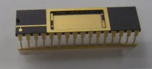
Medical device electronics design encompasses the complete development cycle of electronic systems intended for healthcare environments. Unlike consumer electronics, this design of medical electronic devices requires adherence to strict safety protocols, biocompatibility standards, and regulatory frameworks that govern everything from implantable pacemakers to external diagnostic equipment.
The scope includes circuit architecture, component selection, PCB layout, firmware development, and integration testing—all executed with the understanding that failure is not an option when human lives depend on device performance.
Why Is Medical Device Electronics Design Different From Standard Electronics Design?
| Aspect | Standard Electronics | Medical Device Electronics |
|---|---|---|
| Failure tolerance | Acceptable within warranty terms | Zero tolerance—patient safety critical |
| Regulatory oversight | Minimal compliance required | Strict FDA/CE/ISO 13485 requirements |
| Testing rigor | Basic functional validation | Extensive reliability & safety testing |
| Component grading | Commercial grade acceptable | Medical-grade with full traceability |
| Documentation | Standard technical specs | Comprehensive design history files |
The fundamental difference lies in the consequence of failure. While a smartphone malfunction causes inconvenience, medical device failure can result in serious injury or death. This reality drives every design decision in electronic design medical devices.
What Are the Main Design Requirements for Medical Electronic Devices?
- Safety-first architecture: Redundant systems and fail-safe mechanisms for critical functions
- Biocompatibility compliance: Materials and coatings that prevent adverse tissue reactions
- Electromagnetic compatibility: Immunity to interference and controlled emissions per IEC 60601
- Environmental robustness: Resistance to moisture, sterilization processes, and temperature extremes
- Long-term reliability: 10+ year operational lifespans with minimal maintenance requirements
- Cybersecurity measures: Protection against unauthorized access and data breaches
- Usability engineering: Intuitive interfaces that minimize user error in high-stress situations
How Does the Medical Device Electronics Design Process Work?
The design process follows a structured, iterative approach that prioritizes safety at each stage:
- Requirements analysis: Defining functional specifications aligned with intended use and regulatory class
- Risk assessment: Conducting FMEA (Failure Mode and Effects Analysis) to identify potential hazards
- Schematic design: Creating circuit diagrams with safety margins and redundancy built-in
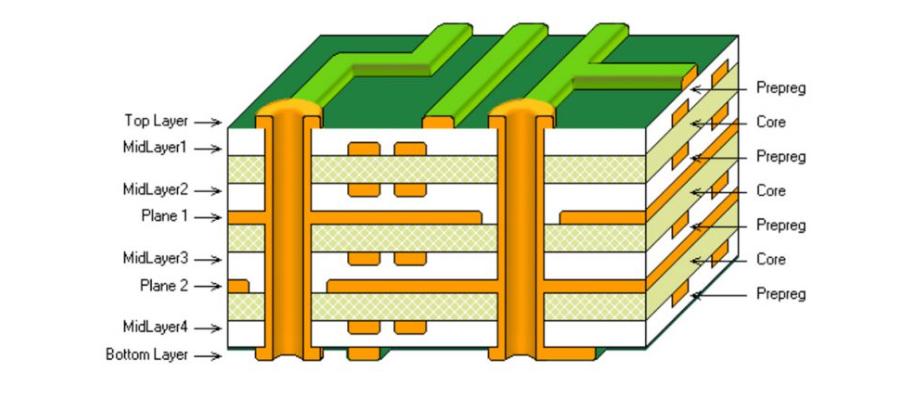
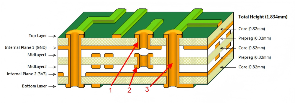
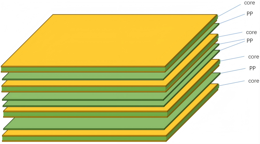
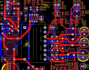
- PCB layout optimization: Routing traces for signal integrity, thermal management, and EMI control
- Prototype development: Building and testing initial units under simulated operating conditions
- Verification & validation: Comprehensive testing against all specified requirements
- Design transfer: Preparing manufacturing documentation and establishing quality controls
Each phase includes documented reviews and approvals, ensuring traceability and accountability throughout the development lifecycle.
Which Standards and Regulations Apply to Medical Electronic Device Design?
Compliance with international standards forms the foundation of safe medical device electronics design:
- ISO 13485: Quality management systems for medical devices
- IEC 60601-1: General safety and essential performance requirements
- IEC 60601-1-2: Electromagnetic compatibility requirements
- FDA 21 CFR Part 820: Quality system regulations for US market
- ISO 14971: Risk management application to medical devices
- IEC 62304: Medical device software lifecycle processes
These standards mandate specific design controls, testing protocols, and documentation practices that ensure consistent safety and reliability across all medical electronic device design projects.
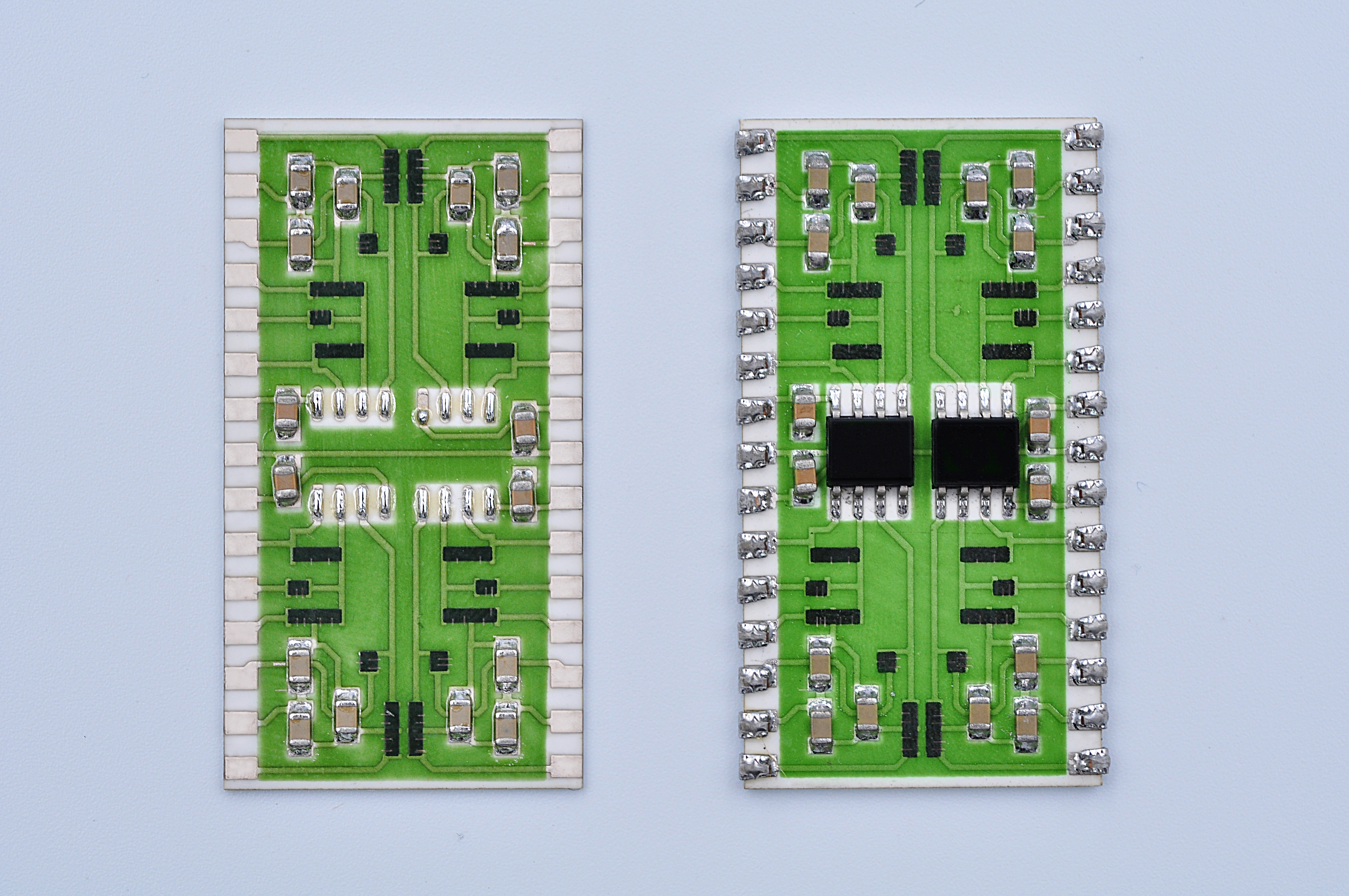
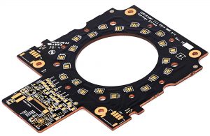
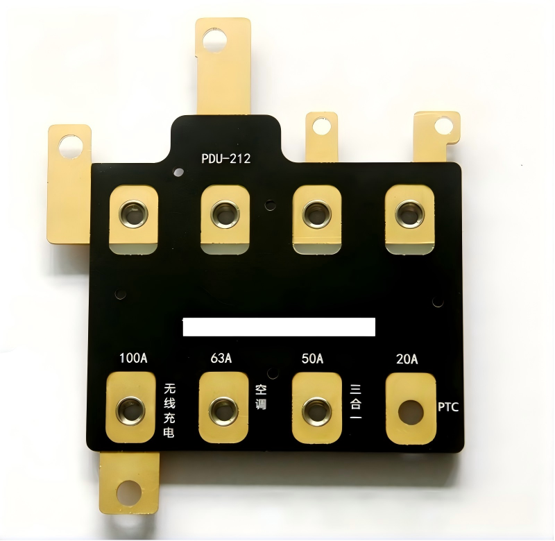
How Do You Design Reliable PCBs for Medical Devices?
Reliable PCB design for medical applications requires attention to several critical factors:
| Design Consideration | Implementation Strategy | Reliability Impact |
|---|---|---|
| Trace width/spacing | Conservative sizing with 50% safety margin | Prevents electrical breakdown |
| Via design | Filled and capped vias for critical signals | Eliminates void formation |
| Copper thickness | 2oz+ copper for power distribution | Reduces thermal stress |
| Solder mask | High-Tg, medical-grade materials | Prevents contamination |
| Surface finish | ENIG or immersion silver | Ensures long-term connectivity |
Additional strategies include implementing guard rings around sensitive analog circuits, using star grounding topologies to minimize noise coupling, and designing for manufacturability to reduce assembly defects.
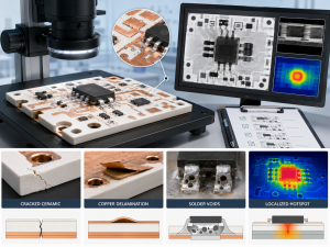
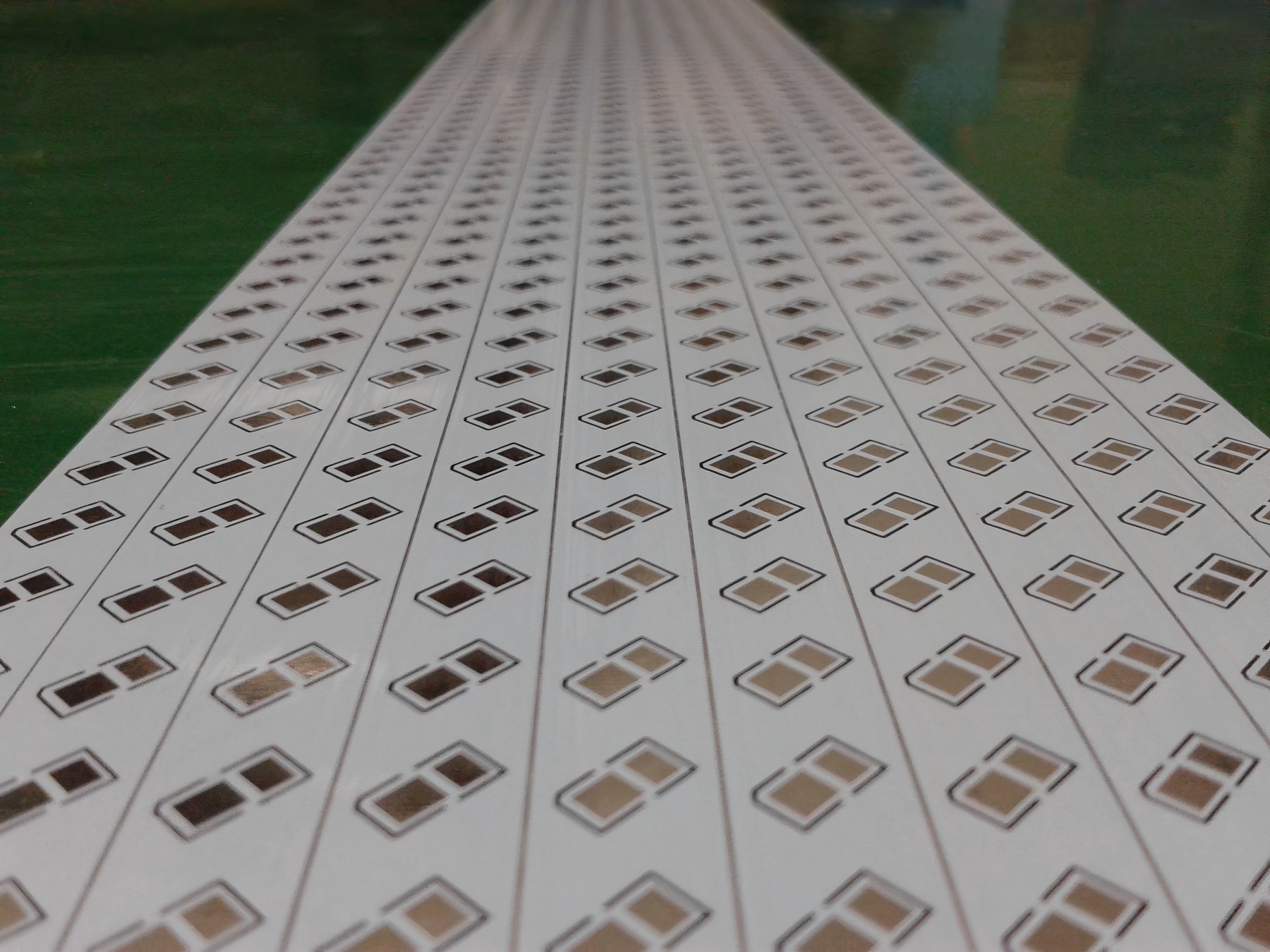
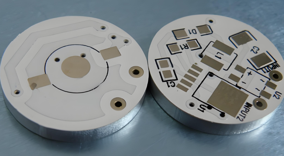
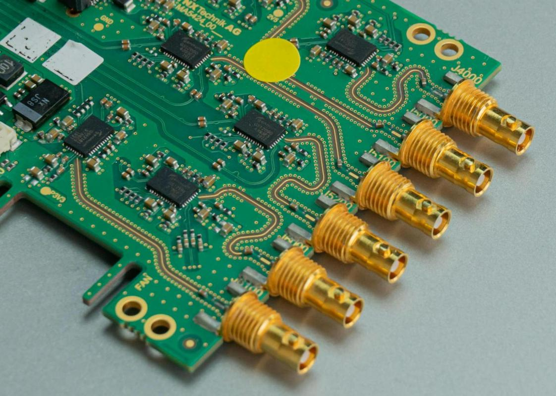
What Are the Common PCBA Challenges in Medical Device Electronics?
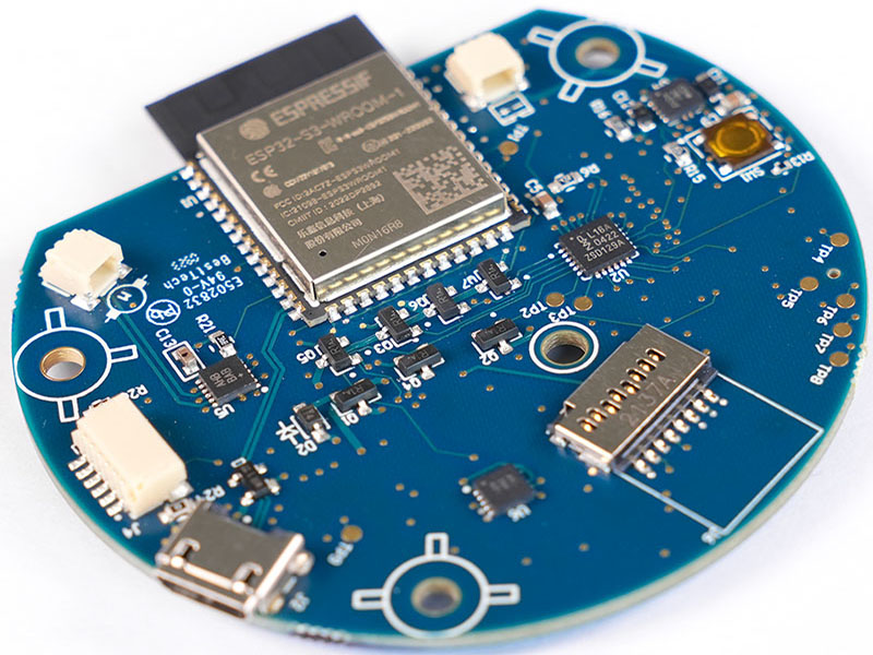
- Fine-pitch component placement: Precision required for BGA and QFN packages in compact designs
- Mixed-signal isolation: Separating analog and digital grounds to prevent noise contamination
- Thermal management: Dissipating heat in sealed enclosures without compromising sterility
- Conformal coating application: Ensuring uniform coverage without masking critical contacts
- Test coverage limitations: Achieving 100% testability in dense, multi-layer assemblies
- Rework constraints: Limited repair options due to contamination concerns and regulatory restrictions
These challenges require specialized equipment, trained personnel, and stringent process controls that exceed typical electronics manufacturing capabilities.
Why Choose EBest Circuit (Best Technology) for Medical Electronics PCB Assembly?
When it comes to the design of medical electronic devices, choosing the right manufacturing partner is critical to ensuring safety and reliability. EBest Circuit (Best Technology) delivers specialized PCB assembly services tailored to the stringent demands of the healthcare industry.
- ISO 13485-Certified Facility: Our quality management system is specifically certified for medical devices, ensuring full compliance with international regulatory standards.
- Advanced SMT Capabilities: We utilize state-of-the-art surface mount technology to handle fine-pitch components, BGAs, and complex layouts required in modern medical device electronics design.
- Rigorous Quality Management: From incoming inspection to final functional testing, we implement multi-stage quality controls to eliminate defects and ensure zero-failure performance.
- Certified Supply Chain Management: We source only medical-grade components with full traceability, mitigating supply chain risks and ensuring material consistency.
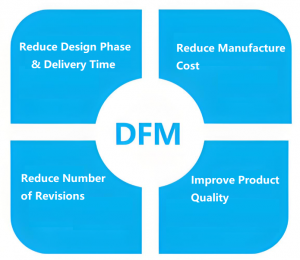
- Design-for-Manufacturability (DFM) Support: Our engineering team collaborates with you early in the electronic design medical devices process to optimize layouts for reliability and cost-effectiveness.
- Full Traceability Documentation: We provide comprehensive documentation and lot tracking to support your FDA/CE submissions and audits.
- End-to-End Project Support: From rapid prototyping to high-volume production, we ensure a seamless transition that maintains the integrity of your medical electronic device design.
Pls feel free to contact us at sales@bestpcbs.com to discuss how we can bring your next medical electronics project to life with uncompromised safety and reliability.
In summary, medical device electronics design ensures safety and reliability through systematic engineering approaches, regulatory compliance, and precision manufacturing processes that prioritize patient welfare above all else. This comprehensive exploration has demonstrated how specialized design methodologies, from initial concept through final assembly, create medical electronic devices that healthcare providers can trust with human lives.
EBest Circuit (Best Technology) stands ready to support your medical electronics development with proven expertise in reliable PCB assembly and regulatory-compliant manufacturing processes. Our commitment to quality and safety makes us the ideal partner for bringing your life-saving innovations to market. Pls feel free to reach out to our team at sales@bestpcbs.com to begin your next medical device electronics design project.
FAQs About Medical Device Electronics Design
1. What are the key regulatory standards for medical electronics design?
Medical electronics must adhere to a hierarchy of international standards to ensure patient safety. The most critical include:
- IEC 60601-1: The primary standard for the safety and essential performance of medical electrical equipment.
- ISO 13485: Specifies requirements for a quality management system (QMS) specifically for medical device manufacturers.
- IEC 62304: Governs the software life cycle processes within medical devices.
- ISO 14971: Defines the application of risk management to medical devices throughout their entire lifecycle.
2. How does EMI/EMC testing affect medical PCB design?
Electromagnetic Interference (EMI) and Compatibility (EMC) are vital because medical devices often operate in “noisy” environments (like hospitals with MRI machines) or must not interfere with other life-critical equipment. Designers must implement:
- Shielding and Filtering: Using ferrite beads, line filters, and physical enclosures to block unwanted signals.
- Strategic Layer Stacking: Utilizing dedicated ground planes in the PCB to minimize loop areas and reduce radiation.
- Component Separation: Keeping sensitive analog front-ends isolated from high-speed digital switching circuits.
3. What are the main challenges in designing wearable medical electronics?
Wearable devices introduce unique constraints that go beyond standard medical equipment:
- Thermal Management: Since the device is in contact with skin, surface temperatures must be strictly controlled to prevent burns (per IEC 60601-1).
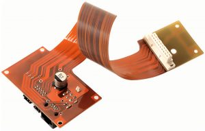
- Miniaturization: Using High-Density Interconnect (HDI) PCBs and rigid-flex circuits to fit complex electronics into ergonomic, small-form-factor housings.
- Power Efficiency: Balancing high-performance sensing with ultra-low power consumption to ensure long battery life for continuous monitoring.
4. What is the difference between design verification and validation in medical electronics?
These are two distinct phases required by the FDA (21 CFR 820.30):
- Design Verification: Answers the question, “Did we design the device right?” It involves testing the electronics against the technical specifications (e.g., checking if the power supply outputs exactly 5V ±1%).
- Design Validation: Answers the question, “Did we design the right device?” This ensures the final product meets the actual needs of the end-user and the patient through clinical trials or simulated use-case testing.