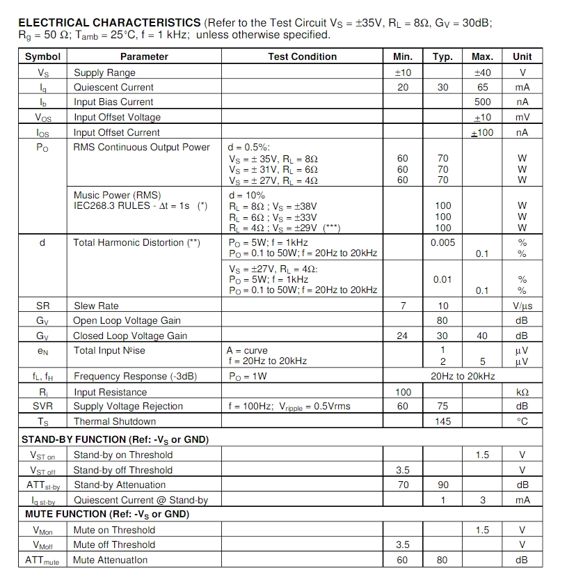
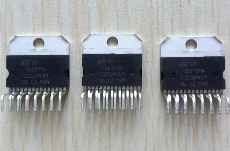
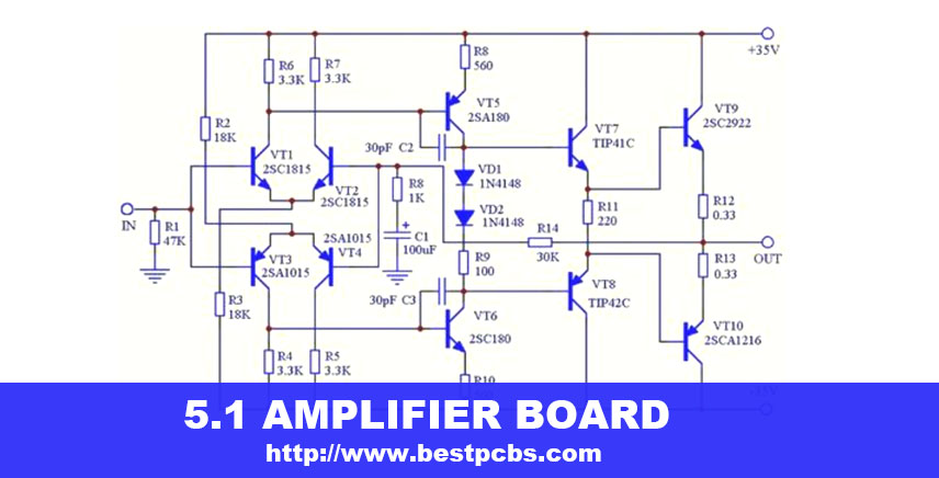
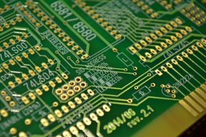
TDA7294 is a class AB monolithic audio amplifier integrated circuit launched by SGS-THOMSON Microelectronics in the 1990s. It swept away the raw, cold and hard sound of previous linear integrated amplifiers and thick film integrated amplifiers, and is widely used in HiFi fields, such as home theaters, active speakers, high-performance TVs and other fields.
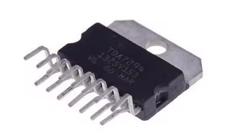
The chip adopts a 15-pin dual-row asymmetric plug-in package, the differential input stage is composed of bipolar transistors, and the driver stage and power output stage use DMOS field-effect transistor semiconductor technology. This hybrid semiconductor manufacturing process allows TDA7294 to take into account the advantages of bipolar signal processing circuits and MOS power tubes, and the playback sound is very friendly (it is praised by audiophiles as a “tube-flavored amplifier”); the built-in silent standby function, short-circuit current and overheating protection functions make its performance more perfect. It can be used in HiFi home audio, active audio, high-performance TVs and other fields.
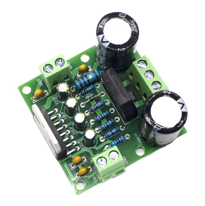
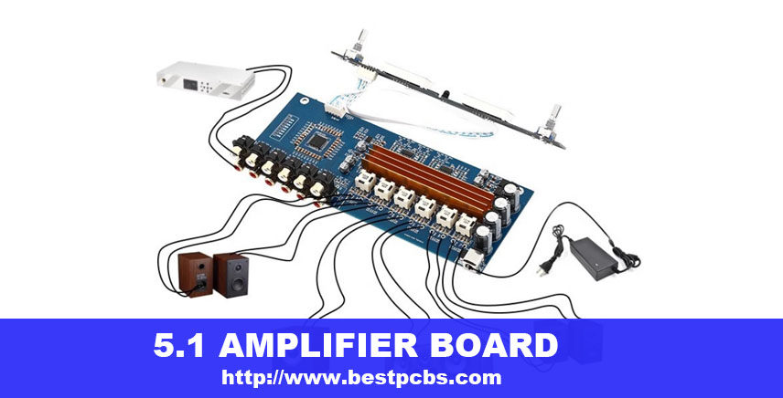
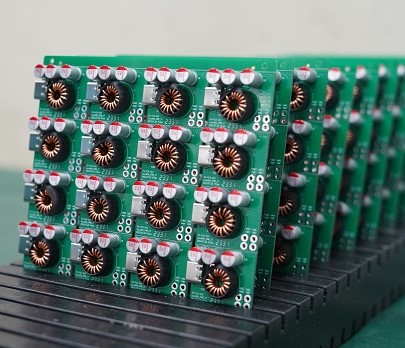
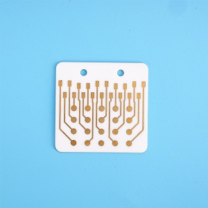
Tda7294 amplifier board
tda7294 amplifier board PCBA
This circuit is an official standard circuit, stable and reliable.
The filter uses a large electrolytic capacitor with a withstand voltage of 50V and a capacity of 2200uf.
Power supply voltage: dual 12-36V ring transformer, dual 32V ring transformer is recommended
Output power: 85W*1 undistorted rated power, peak power 100W
Can easily drive speakers above 100W, speaker impedance: 4-8 ohms
PCB size: 50*50mm
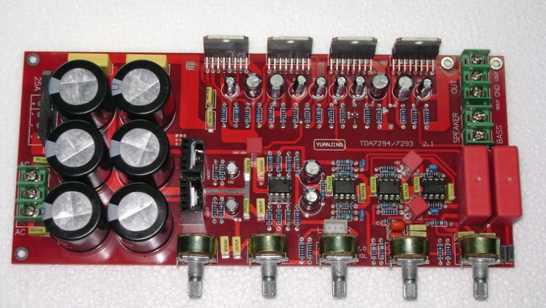
Basic parameters: Power supply: dual 18-28V AC Power: 2X80W+160W subwoofer Circuit board size: 218x98MM Potentiometer function: low frequency frequency adjustment, subwoofer volume. Left and right channel volume, treble, bass.
Adopting the new laser dark word TDA7294 The power filter uses 6 63V3300UF capacitors, and the rectifier uses a 25A imported rectifier flat bridge. PCB uses 1.6mm thick double-sided board, 2.0 ounces copper thickness, and full tin spraying process to ensure good passing performance of large and small currents. Fever component assembly, the subwoofer part consists of two new TDA7294 BTL output, The low-pass filter is designed according to the frequency adjustable design of home theater style (50-150HZ), with strong power! The left and right channels are served by two TDA7294 respectively, and the input coupling capacitor uses the German imported WIMA 2.2UF coupling capacitor, which makes the sound sweeter! The signal-to-noise ratio of the board is also very high, and even if you put your ear close to the speaker, you can’t hear the AC noise! It is the best choice for upgrading 2.1 amplifiers!
TDA7294 datasheet
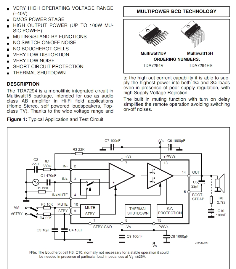
TDA7294 Main Features
Wide supply voltage range: ±10V ~±40V High output power: 70W (up to 100W) Standby and mute functions Noiseless ON/OFF switch Low noise and low distortion Short circuit protection and overheat protection
TDA7294
Pin function Pin 1 is the standby terminal; Pin 2 is the inverting input terminal; Pin 3 is the positive input terminal; Pin 4 is grounded; Pins 5, 11, and 12 are empty pins; Pin 6 is the bootstrap terminal; Pin 7 is +Vs (signal processing part); Pin 8 is -Vs (signal processing part); Pin 9 is the standby pin; Pin 10 is the mute pin; Pin 13 is +Vs (final stage); Pin 14 is the output terminal; Pin 15 is -Vs (final stage)
DIY Production
1) The first step is to get the PCB. Here you can make the PCB yourself by DIY ironing method. Since the PCB is easy to make, the PCB design is kept single layer only, or you can get ready-made quality PCB from best.or custom tda7294 amplifier board. 2) After the PCB is completed, carefully mount all small components like jumpers, resistors, diodes, etc. to the PCB and trim their terminals, then solder them to the PCB first, because there are many components on this board, so it is better to solder them one by one 3) After installing the small components, install the large components like capacitors, fuse holders, rectifiers to the PCB and solder them. (Don’t install the power filter capacitor, 22000uF capacitor for now. Completed in the following steps) 4) After that, it’s time to mount all 7 ICs to the PCB and solder them. 5) Now properly mount the heat sink on the IC using insulating MICA and insulating plastic shoulder washers. Remember to use good quality thermal paste between the heat sink and IC. 6) After mounting the IC on the heat sink. Check the continuity between the heat sink and the IC back plate using a multimeter. There should not be any continuity between them. Please note the heat sink isolation 7) Now mount the cooling fan to the PCB using cable ties or any other suitable method. The board assembly is now complete. Clean the track side of the board using IPA (Isopropyl Alcohol) or cleaning flux and then power the board using a 20-0-20 VAC transformer or a 24-0-24 VAC transformer.
Which one has better sound quality, TDA7294 or LM3886? Voltage AC 28v
LM3886 has better bass because its maximum current can reach 10A, which means it can drive a 2-ohm box without any problems. From the parameters alone, LM3886 is worse than 7294. And it is true in practice, especially for bass. If the transformer is OK, it feels very powerful. 7294 is not as good as 3886 in bass. The current is large when it comes to bass. 7294 itself has overcurrent protection. When the current reaches a certain level, it starts to limit the output current. However, 7294 is better in treble.
In the imperial system, 12 inches is 1 foot, and 36 inches is 1 yard. 1mil=1/1000inch=0.00254cm=0.0254mm. 1inch=2.54cm=25.4mm=1000mil 1 inch=2.54cm=25.4mm.
10 mm = 0.393700787 inches 50 mm =1.96850394 inches
1400mm in inches 1400 mm = 55.1181102 inches
1500 mm to inches 1500 mm = 59.0551181 inches
1800mm to inches 1800 mm =70.8661417 inches
Origin of the inch
The word “inch” comes from the Old English word “ynce”, which comes from the Latin word “uncia” (meaning “one twelfth”). In the 14th century, King Edward II of England promulgated the “standard legal inch”; its regulations were: the length of the three largest grains of wheat selected from the middle of the barley ear and placed end to end in a row is 1 inch.
mm or inches in the PCB industry
(including the substrate and all copper layers, solder mask and silk screen), either millimeters or inches can be used as units. However, 1.6 mm is not the only choice, and the thickness of the PCB can vary depending on the specific application, ranging from 0.3 mm to 4.0 mm1. In PCB design, for design and layout units such as traces, pads, spacing and grids, the imperial unit “thou” (one thousandth of an inch) should be used instead of millimeters. For mechanical manufacturing unit requirements such as apertures and PCB board sizes, millimeters can be used. This shows that when designing PCBs, you need to be familiar with the conversion relationship between the imperial unit “thou” and the metric unit millimeter. In summary, the units used in the PCB industry depend on the specific application scenarios and requirements. When describing the thickness of the PCB board, millimeters or inches can be used as units, while in design and layout, the imperial unit “thou” should be used to adapt to design requirements.
PCB package size
PCB length units usually refer to the shortest distance between components on the PCB. Common length units are inches, centimeters and millimeters. For example, the minimum PCB length unit for the 0805 package size is 1 inch, while the minimum PCB length unit for the 0402 package size is 0.25 inches. In addition, there are some other commonly used PCB package sizes, such as 0101 package size, 0201 package size, 0302 package size, etc.
PCB package size is a standard size for mounting and connecting electronic components on PCBs. The following are the most commonly used device PCB package sizes: 1.0805 package size: This package size is used for electronic components of 8 inches (about 20 cm) in size, including transistors, capacitors, inductors and other small components. 2.0402 package size: This package size is used for electronic components with a size of 4 inches (about 10 cm), including transistors, capacitors, inductors and small components. 3.0603 package size: This package size is used for electronic components with a size of 6 inches (about 15 cm), including transistors, capacitors, inductors and small components. 4.1206 package size: This package size is used for electronic components with a size of 12 inches (about 30 cm), including transistors, capacitors, inductors and small components.
The unit of PCB length is usually millimeter (mm) or inch (inch), while the unit of copper foil thickness is OZ (ounce), which is about 35um or 1.35mil. When designing the PCB of the op amp circuit, factors such as layout, wiring, power decoupling, and heat dissipation design need to be considered to ensure signal integrity and stability.
A 5.1 amplifier boardis a sound amplifier that can expand the current and voltage of an audio signal to make the sound louder. In addition, a 5.1 amplifier board also has a multi-channel processing function, which can output audio signals through multiple channels to enhance the sound field effect, making listening to music, watching movies, etc. more three-dimensional and realistic. Compared with traditional 0 and 1 amplifiers, in addition to being able to connect two front speakers and two rear speakers, a 5.1 amplifier board can also connect a center speaker and a subwoofer, making the bass of music or movies more prominent and the sound deeper. 5.1 amplifiers are widely used in home theater systems. By combining with projectors, TVs and other equipment, a theater environment with excellent audio-visual effects can be created. In addition, for music lovers, a 5.1 amplifier board is also an indispensable device that can not only maximize the effect of music, but also allow people to experience the charm of music in an immersive way.
5.1 Basic parameters of the amplifier board
Working mode: Class D Quiescent current: 50mA Working efficiency: 90% Rated output power: 2200W+400W Frequency response: 20Hz to 20KHz Working voltage: DC24V-42V( Recommended voltage: DC42V Maximum output current: 10A PCB size: 114109MM Potentiometer center distance: 21.5MM 21.5MM 21.5MM from left to right Original TPA3223 is used
TPA3223 2.1 Digital Bluetooth 5.1 3034 Amplifier Board
1.The front input capacitor and interstage coupling capacitor use ELNA BP capacitor 10UF, the electrolytic capacitor signal main circuit uses Taiwan famous brand, and the main filter capacitor uses imported electrolytic capacitor 1000UF , ensuring strong and continuous power support. 2.The resistors are made of high-precision chip resistors, and the main circuit uses a five-ring metal film resistor with an accuracy of ±1%, which ensures a good signal-to-noise ratio for the whole machine. 3.The PCB uses a 1.6mm thick double-sided board, 2.0 ounces of copper thickness, and a full tin-spraying process to ensure good passing performance of large and small currents. 4.The fully enclosed dust-proof potentiometer is used, which has more stable performance and is more durable than ordinary potentiometers. 5.The red-gray ring high-current inductor and the fully shielded audio-specific output inductor are used to ensure a crisp and powerful sound. The Bluetooth uses Qualcomm QCC3034 5.1 version Bluetooth module
5.1 amplifier board of working principle
The core function of the amplifier board is to increase the amplification factor of the signal while protecting the circuit from damage. The amplifier board is usually used for isolation and current amplification between the programmable logic controller (PLC) and the input device or output device to improve the load capacity of the PLC and protect the PLC from faults such as overvoltage, overload, and load short circuit.
The working principle of the amplifier board is based on the amplifier circuit, using electronic components with amplification characteristics, such as transistors. When the tiny current at the input end changes, a large current change will occur at the output end, and the change at the output end is several to hundreds of times greater than the change at the input end. The characteristic of this amplifier circuit is that only one potential point is amplified, and the other potential point is grounded by default. In addition, the integrated circuit (IC) is also an important part of the amplifier board. It integrates many transistors, resistors, capacitors and other components on a small piece of semiconductor silicon single crystal, and uses isolation technology to insulate them from each other in electrical properties, thereby realizing signal amplification and processing.
For example, an analog signal amplifier board can connect multiple sensors, collect differential signals and amplify them to the required multiples through an amplifier circuit. The board can work normally in the temperature range of -15℃ to 70℃, and the humidity can reach 90%, which is suitable for various harsh environments. This amplifier board is widely used in industrial automation, smart home, medical equipment and other fields to ensure stable signal transmission and processing
The role of the amplifier board
The main functions of the amplifier board:
This is because some process control equipment such as proportional valves can only receive analog voltage or current signals. Therefore, in order to ensure that these devices can correctly receive and respond to the signals sent by the PLC, an intermediate amplification link, namely the amplifier board, is required. It can properly amplify the signal output by the PLC D/A module to make the proportional valve work normally.
The amplifier board is also called the IO relay board. Its main functions include isolation, current amplification, and providing additional I/O channels. It can improve the load capacity and reliability of the PLC system and prevent the PLC host from being damaged due to overvoltage, overload or load short circuit.
The amplifier board is widely used in the field of industrial automation. It can not only improve the load capacity and reliability of the PLC system, but also protect the output or input points of the PLC.
The amplifier board can save cabinet space, increase installation speed, facilitate maintenance and replacement, and has protection circuits and built-in insurance, which makes it difficult to damage the amplifier board itself and the load.
The amplifier board can also play the role of amplifying interference, because its input and output are photoelectrically isolated, and the PLC will not be burned out due to high-voltage impact load. These features make the amplifier board play a vital role in industrial automation systems.
Application of 5.1 amplifier board
5.1 channel amplifiers are mainly used in home theater systems to provide surround sound audio output and an immersive listening experience for the audience. 5.1 channel amplifiers are an indispensable component of home theater systems. They can provide five full-band channels and one low-frequency effect channel. Through carefully designed audio processing, the audience can feel the sound from different directions, thereby enhancing the immersion of movies or concerts.
In addition to home theater applications, 5.1 channel amplifiers are also suitable for professional audio systems, such as conference rooms, performance venues, etc., where high-quality audio output is required. In these occasions, 5.1 channel amplifiers can ensure stable signal transmission and high-quality restoration to meet professional-level audio needs.
In short, the 5.1 channel amplifier board provides multi-channel audio output, bringing a more realistic and three-dimensional sound experience to viewers or listeners, playing an important role in both home entertainment and professional applications.
FAQs About 5.1 amplifier board
Does the 5.1 amplifier front panel consist of 6 front panels?
A true 5.1 should have 6 input interfaces (marked as: 5.1IN) and 6 speakers including a subwoofer.
5.1 is an independent 6-channel amplification and 6-channel speaker restoration, and of course an independent 5.1-channel sound source is required.
The 5.1 speaker requires the amplifier to have an independent 6-channel amplifier. Virtual ring. Winding into multiple channels
How many power amplifiers are there in a 5.1 channel amplifier? Two situations, the first is 5.1 full-channel power amplification, that is, 6 channels, but in this case the power of the bass channel is small, which can drive 6~8-inch bass, but it can’t drive large ones. The second is 5-channel power amplification, except for the bass channel, the other channels are power amplified, the bass channel only provides a level signal, and the signal enters the active subwoofer amplifier board to drive the subwoofer, which is more common.
Can the 5.1 channel amplifier board use dual DC?
Ordinary transistor power amplifiers use DC. What do you mean by “using dual DC power”? Does it mean using a backup power supply? … Using a backup power supply is completely possible.
In addition, there are power amplifiers that are powered by [positive and negative symmetrical power supplies]. Such power amplifiers must use DC positive and negative symmetrical power supplies.
Can I make a 5.1 with two 2.1 amplifier boards?
One of them is used for 2.1 (the analog subwoofer circuit is removed as bass amplification), and the other is used for surround channels (remove the subwoofer circuit and change to center). After merging, it is 5.1. The 6 amplification channels must be connected to the 5.1 decoding output.
Can a 5.1 pre-stage board be used with a 2.0 amplifier? It can definitely be used. The pre-stage board only plays the role of audio adjustment and does not perform power amplification. The input audio signal can be connected to the amplifier after being adjusted and output by the pre-stage board. For the 5.1 channel, just select 2 of the output signals.
When communicate with clients, they always ask why the PCB board are so expensive? Is there any basis for that? Actually, the price of PCBs are made specifically according to its manufacturing process, layers, complexities and so on. Today, EBest Circuit (Best Technology) is deeply sharing the composition of PCB cost. Welcome to keep reading.
Why is PCB Board So Expensive?
The cost of a PCB can sometimes seem high due to several reasons. Firstly, the complexity of the design plays a significant role. High-density interconnect (HDI) PCBs, multi-layer PCBs, and those requiring advanced materials or special finishes can drive up the cost. Additionally, stringent quality control measures and the need for precise manufacturing processes add to the expense.
Another factor is the cost of raw materials. Copper, laminates, and specialty substrates can vary in price, affecting the overall cost of the PCB. Furthermore, labor costs in the region where the PCB is manufactured, along with overhead costs such as utilities and facility maintenance, contribute to the final price.
What Factors Affect the PCB Board Cost?
PCB board can cost from $10 to $500 to produce. Buyers are always amazing that why PCB cost so high? But they don’t know there are numerous factors a manufacturer considers in determining PCB costs. If you are in the market to design a PCB, this guide provides factors to consider that could increase or decrease the cost of circuit boards.
Manufacture technology
The specific technology used in the PCB can significantly impact the cost. Advanced technologies such as HDI (High-Density Interconnect), embedded busbar or flexible PCBs often require more complex manufacturing processes, which can increase the cost.
Material Type
The type of materials used for the PCB, such as standard FR4, high-frequency laminates, or other specialty substrates, can influence the cost. Higher quality or specialized materials typically cost more.
IPC Grade
The IPC standards and grades indicate the quality and reliability requirements of the PCB. In electronics manufacturing, printed circuit boards are divided into three levels: level 1, level 2 and level 3. These grades reflect the quality level of each board type, from the lowest (Level 1 standard) to the highest (Level 3 standard). This classification system was developed and defined by IPC and is specified in the IPC-6011 series.
Circuit Design
The complexity of the circuit design, including the number of layers, trace width, and spacing, affects the cost. More intricate designs require more precision and advanced techniques, leading to increased expenses.
PCB Size & Yield
The physical dimensions of the PCB and the yield rate during production play a role in the overall cost. Larger boards or designs with lower yield rates (more defects) will typically cost more to produce.
Material Thickness
The thickness of the materials used in the PCB construction, such as the substrate and copper layers, can impact the cost. Thicker materials may be more expensive and require more resources to process.
Copper Thickness
The thickness of the copper used in the PCB, measured in ounces per square foot, can affect the cost. Thicker copper layers provide better electrical performance but are more expensive.
Stack-up
The method of layering and stacking the materials in the PCB, known as the stack-up configuration, can influence the cost. Complex stack-ups with multiple layers and specific arrangements can be more costly to manufacture. Read our another post of How Can I Reduce and Optimize the Cost of My PCB in A Best Way?
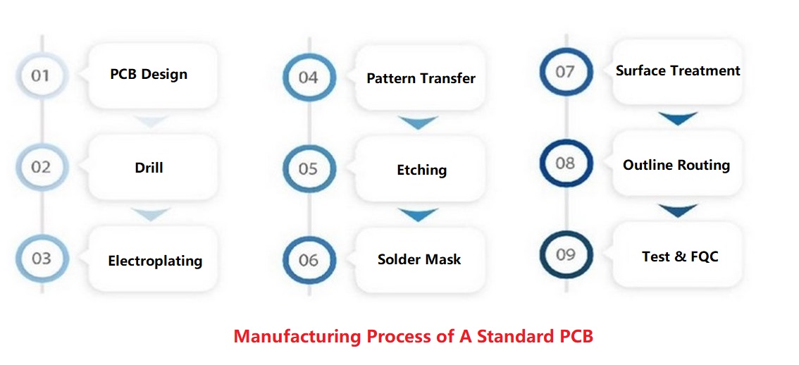
Manufacturing Process of A Standard PCB
PCB Design and Layout
The manufacturing process begins with the design phase, where engineers use CAD (Computer-Aided Design) software to create the PCB layout. This includes defining the circuit paths, components, and layers, ensuring the design meets the electrical and mechanical requirements.
Once the design is finalized, a photomask is created, which is a transparent film with the PCB design printed on it. The PCB substrate, typically made of FR4, is then coated with a light-sensitive material called photoresist.
Drilling
Precise holes are drilled into the board for through-hole components and vias using computer-controlled drilling machines. The board is cleaned and deburred to remove any rough edges or debris from the drilling process.
Plating and Copper Deposition
A thin layer of copper is deposited on the surface of the board and inside the drilled holes through an electroless plating process, providing a conductive base. Additional copper is electroplated onto the board, building up the thickness of the copper traces and plated through-holes.
Pattern Transfer
The photomask is placed over the photoresist-coated substrate and exposed to ultraviolet (UV) light. The UV light hardens the photoresist where the design allows light to pass through, and the board is then developed to wash away the unhardened photoresist, leaving behind the desired circuit pattern.
Etching
The PCB undergoes an etching process using a chemical solution to remove unwanted copper, leaving only the copper traces that form the circuits. The remaining hardened photoresist is then stripped away to reveal the clean copper pattern.
Applying Solder Mask
A layer of solder mask is applied to the board to protect the copper traces from oxidation and prevent solder bridges during assembly. The solder mask is cured using UV light, hardening it and making it durable.
Surface Finish/Surface Treatment
A surface finish is applied to the exposed copper areas to protect them and facilitate soldering. Common finishes include HASL (Hot Air Solder Leveling), ENIG (Electroless Nickel Immersion Gold), and OSP (Organic Solderability Preservatives).
Outline Routing
One the surface treatment finish, it will be routed according to the manufacturing file by CNC machine. And then individual PCBs are cut from the larger panel using routing or V-scoring, depending on the board design and requirements.
Electrical Testing & FQC
The PCB undergoes electrical testing to check for short circuits, open circuits, and other defects. This is typically done using a flying probe tester or a bed-of-nails tester. Then the board is visually inspected for any cosmetic defects or anomalies, and further tests and inspections are performed to ensure the PCB meets all specified requirements and standards. Below you can see the full manufacturing process video of a PCB:
EBest Circuit (Best Technology) – A 18+ Years Experience PCB Manufacturer
When you are looking for a reliable PCB manufacturer, considering EBest Circuit (Best Technology). We have transparent price and 5years quality warranty. We 24/7 hours online and welcome all the technical questions and PCB inquiries. Contact us for more!
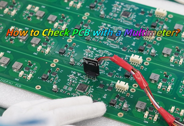
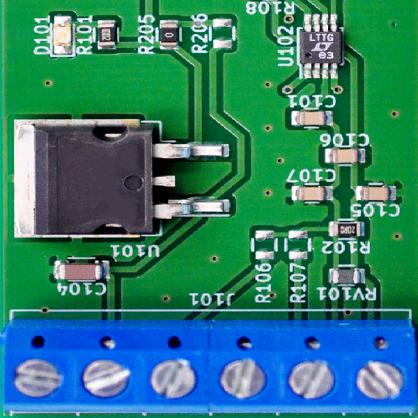
Common PCB failures are mainly concentrated on components such as capacitors, resistors, inductors, diodes, transistors, MOSFETs, integrated chips (IC), and crystals. Some obvious damages can be visually detected, while others require the use of tools. Today, let’s learn how to troubleshoot PCB faults using a multimeter.
How Will You Diagnose a Faulty PCB By Visually?
For some printed circuit boards, we can check by our naked eyes. Here are some common ways to follow:
1. Check the condition of components
When you get a faulty PCB, first observe if there are any obvious component damages, such as burnt or swollen electrolytic capacitors, burnt resistors, and damaged power devices.
2. Inspect the soldering of the PCB
Check if the printed circuit board (PCB) is deformed or warped; if there are any loose or poorly soldered joints; if the copper cladding on the PCB is lifted, burnt, or blackened.
3. Examine the component plug-ins
Ensure the correct orientation of integrated circuits, diodes, and the PCB power transformer.
How to Check PCB with a Multimeter?
Before you start testing your PCB, ensure you have the right tools and environment. Here’s a checklist to get you started:
1. Safety First: Wear anti-static gloves and ensure you are working on an anti-static mat to prevent damage to the PCB.
2. Multimeter Selection: Choose a multimeter with the ability to measure voltage, resistance, and continuity. A digital multimeter is preferred for accuracy.
3. Visual Inspection: Examine the PCB for visible signs of damage such as burnt components, broken traces, or solder bridges.
4. Power Off the Board: Always test the PCB with the power off to avoid any electrical hazards and damage to the multimeter.
How Do You Test Individual Components on a PCB?
Testing individual components like resistors, capacitors, and diodes can pinpoint the exact failure. Here’s a general approach:
Diode
Transistor
MOSFET
Electrolytic Capacitors
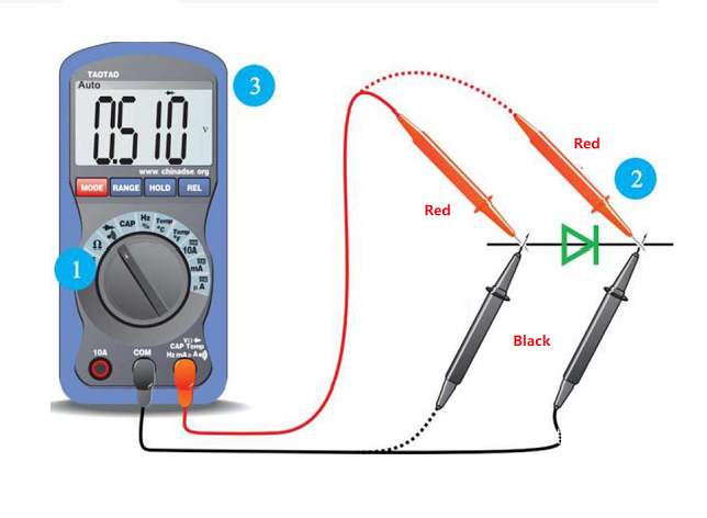
How to Test Diodes?
1. Set the MF47-type multimeter to measure resistance.
2. Place the red and black probes on the two ends of the diode and read the value.
3. Swap the probes and measure again.
4. Judge based on the two measurements: the forward resistance of small power germanium diodes is 300-500Ω, silicon diodes are about 1kΩ or larger. The reverse resistance of germanium diodes is tens of kilo-ohms, and silicon diodes are above 500kΩ (values are much smaller for high-power diodes). A good diode has low forward resistance and high reverse resistance, and the larger the difference, the better.
5. If both forward and reverse resistances are very low, the diode is short-circuited; if both are very high or infinite, the diode is open-circuited and needs to be discarded.
How to Test Transistors?
1. Set the digital multimeter to the diode mode.
2. Measure the PN junction with the probes. If it conducts forward, the displayed value is the forward voltage drop of the PN junction.
3. Determine the collector and emitter: measure the forward voltage drop of the two PN junctions, the larger drop is the emitter (e), and the smaller drop is the collector (c). If the red probe is connected to the common terminal, the transistor is NPN type, and the common terminal is the base (b); if the black probe is connected to the common terminal, the transistor is PNP type, and the common terminal is the base (b).
4. For in-circuit testing, measure the forward and reverse resistance of the PN junction to determine if the transistor is damaged. If the branch resistance is larger than the forward resistance of the PN junction, there should be a clear difference between the forward and reverse resistances, otherwise, the PN junction is damaged.
The Way to Test MOSFETs?
1. Connect the black probe to the drain (D) and the red probe to the source (S), the resistance should be 500-600.
2. Without moving the black probe, touch the gate (G) with the red probe, then measure the source (S) again; it should conduct.
3. Connect the red probe to the drain (D), touch the gate (G) with the black probe, then measure the source (S); the resistance should be the same as the first measurement, indicating the MOSFET is working normally.
How to Test Electrolytic Capacitors?
1. Select the appropriate range on the MF47-type multimeter based on the capacitor’s capacity. Use R×1K range for capacitors below 47μF, and R×100 range for those above 47μF.
2. Connect the red probe to the negative lead and the black probe to the positive lead of the capacitor.
3. On initial contact, the multimeter needle will deflect right and then gradually return to the left until it stops at a certain position (close to infinity). This value is the capacitor’s forward leakage resistance; the larger the value, the better the capacitor’s performance.
4. Swap the probes and repeat the process. The measured value will be the reverse leakage resistance, slightly smaller than the forward leakage resistance.
5. If no charging phenomenon occurs (the needle doesn’t move), the capacitor is either open or short-circuited internally. If the resistance is very small or zero, the capacitor is leaky or has broken down and cannot be used.
This is the end of this article, if you want to know more about it, welcome to contact us.
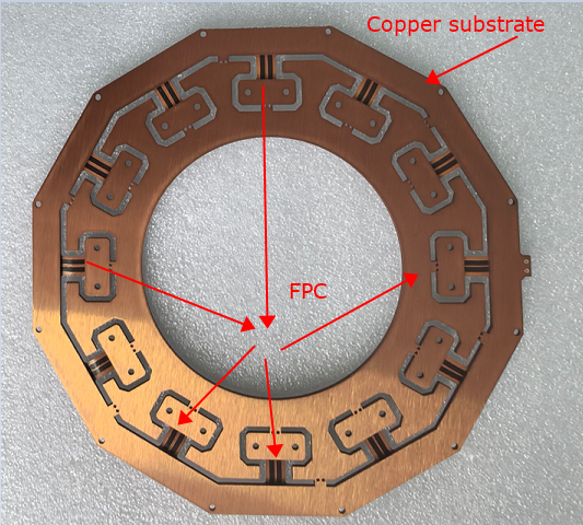
As electronic devices become increasingly miniaturized and high-performance, traditional circuit boards are no longer sufficient for certain high-demand applications. To address these challenges, the Thermal-Electric Separation Copper Substrate with Flexible PCB has emerged. This innovative composite circuit board combines the efficient heat dissipation characteristics of thermal-electric separation copper substrates with the flexibility of flexible PCBs (FPC). It is widely use for high-performance electronic products, which requires efficient heat dissipation and complex circuit.
What is Thermal-Electric Separation Copper Substrate with Flexible PCB?
The Thermal-Electric Separation Copper Substrate with Flexible PCB is a composite material that combines a rigid thermal-electric separation copper substrate with a flexible circuit board. It integrates the advantages of both, providing superior performance in high-power and high-density applications.
1. Thermal-Electric Separation Copper Substrate
The thermal-electric separation copper substrate is designed for high-power electronic devices, providing an efficient heat dissipation solution. It separates the paths of heat and electrical signals to avoid thermal interference with electrical performance. Its structure typically includes:
Single-sided design: Electronic components are placed on one side of the copper substrate, while the other side is used for heat dissipation.
High thermal conductivity materials: Such as copper or aluminum, which can quickly conduct heat, like copper is 400W/m.k, aluminum is 237W/m.k.
Thermal vias: Vertical heat conduction paths that rapidly transfer heat to the dissipation layer.
2. Flexible PCB (FPC)
Flexible PCBs (Flexible Printed Circuits, FPC) use flexible materials like polyimide (PI) or polyester (PET) that can bend and fold to adapt to complex three-dimensional structures and dynamic application scenarios. Their advantages include:
Lightweight: Reducing the overall weight of the device.
High-density wiring: Achieving complex circuit designs in limited space.
Flexibility: Meeting diverse design needs.
Structure and Characteristics
The structure of the Thermal-Electric Separation Copper Substrate with Flexible PCB includes rigid and flexible parts, connected together using conductive adhesives or other bonding materials to form a unified whole.
1. Rigid Part
The rigid part uses the thermal-electric separation copper substrate, responsible for efficient heat dissipation and mechanical support. This part usually carries high-power components to ensure rapid heat transfer and dissipation.
2. Flexible Part
The flexible part uses the flexible PCB, which can bend and fold to fit the complex internal structure of devices. This part is typically used to connect the rigid part with other modules that require flexible connections.
3. Bonding Method
The flexible and rigid parts are bonded together using conductive adhesives, welding, or mechanical connections. The design of the bonding area ensures stable electrical connections and reliability during bending and dynamic use.
Thermal-Electric Separation Copper Substrate with Flexible PCB Advantages
1. Efficient Heat Dissipation
The thermal-electric separation copper substrate provides excellent heat dissipation, effectively conducting away the heat generated by high-power components to maintain a reasonable operating temperature range. This is especially important for applications like high-power LEDs and power semiconductor devices.
2. Flexibility
The use of the flexible PCB offers great design freedom, allowing adaptation to the complex three-dimensional structures and dynamic application needs within devices. This enables designers to achieve more complex circuit designs in limited spaces, increasing device integration and functionality.
3. Reliability
The thermal-electric separation design and high thermal conductivity materials enhance the reliability of the circuit board, reducing the impact of heat on electrical performance. The flexible part reduces the number of connection points, lowering the risk of failure.
4. Space Saving
Combining the advantages of rigid and flexible circuit boards allows for efficient heat dissipation and complex circuit in limited space. This is crucial for modern miniaturized and high-density electronic product designs.
Where Thermal-Electric Separation Copper Substrate with Flexible PCB used?
1. High-Power LED Lighting
High-power LEDs generate a significant amount of heat during operation. The thermal-electric separation copper substrate provides an efficient heat dissipation solution, ensuring the stable operation and long lifespan of LEDs. The flexible part is used to connect different LED modules, accommodating diverse design requirements.
2. Automotive Electronics
In automotive electronics, such as in-vehicle cameras and sensor modules, efficient heat dissipation and compact design are required. The thermal-electric separation copper substrate with flexible PCB can meet these demands, enhancing device reliability and performance.
3. Consumer Electronics
Devices like smartphones and tablets require lightweight and miniaturized designs. The thermal-electric separation copper substrate with flexible PCB offers efficient heat dissipation and flexible circuit, optimizing device performance and user experience.
4. Medical Devices
In applications that require flexibility and reliability, such as portable diagnostic equipment and implantable medical devices, the thermal-electric separation copper substrate with flexible PCB can help to enhancing device performance and reliability.
How does Thermal-Electric Separation Copper Substrate with Flexible PCB manufactured?
The manufacturing process for the thermal-electric separation copper substrate with flexible PCB is complex, typically including the following steps:
Material Preparation: Selecting appropriate rigid and flexible materials and performing pre-treatment.
Circuit Printing: Printing circuit patterns on both rigid and flexible materials.
Lamination and Bonding: Combining the flexible circuit board with the thermal-electric separation copper substrate, usually using conductive adhesives or other bonding materials.
Drilling and Plating: Drilling holes and electroplating to form conductive paths on the combined board.
Surface Treatment: Performing surface treatments such as pad coating on the circuit board.
Testing and Inspection: Conducting electrical and mechanical performance tests to ensure the quality and reliability of the board.
The thermal-electric separation copper substrate with flexible PCB, as an innovative composite circuit board, combines the advantages of efficient heat dissipation and flexible wiring. It is widely used in high-performance and complex design electronic products. With continuous technological advancements and growing market demand, this composite circuit board will play an important role in more fields, driving the ongoing innovation of electronic manufacturing technology. Want know more about it, just feel your free to contact us.
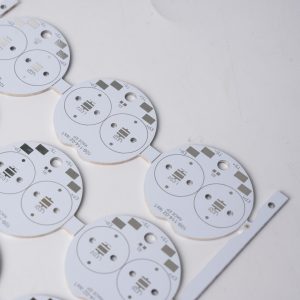
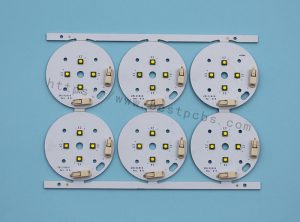
led ring light pcb leads the development of lighting industry with its innovative design, high efficiency and flexibility, bringing more intelligent and comfortable lighting experience to our life.
It is not only an integrated platform of electronic components, but also a perfect combination of modern technology and aesthetics, and is the focus of future lighting trends.
led ring light pcb, like a magic wand on the electronic stage, uses precise SMT technology to lightly attach LED components to it. Whether it is a warm small lamp for home decoration, efficient lighting in commercial space, or smart display inside the car, it is indispensable.
Its core structure includes efficient LED lamp beads, power cords that provide electricity, and intelligent controllers that adjust light effects, which together build an excellent lighting solution.
What Is led ring light pcb
Why use mcpcb for led ring light pcb
With the continuous development of LED technology, the heat generated by LEDs has gradually increased. The traditional FR4 printed circuit board (PCB) has been unable to meet the heat dissipation requirements due to its low thermal conductivity (only 0.36W/m.K). In order to solve this problem, the metal core printed circuit board (MCPCB) was proposed. It attaches the original printed circuit board to a metal with better thermal conductivity (such as aluminum and copper) to enhance the heat dissipation effect. The thermal conductivity efficiency of MCPCB is higher than that of traditional FR4 PCB, reaching 1W/m.K to 2.2W/m.K, which effectively improves the heat dissipation performance of LED PCB.
In addition, the use of MCPCB can also reduce the number of LEDs required to generate lighting, making it an ideal choice for street lights, automotive LED applications, and backlight unit applications. The use of metal substrates has practical advantages in heat dissipation, thermal conductivity, reliability, and electrical insulation, especially in harsh environments, and can also achieve reliable operation of LEDs. For example, using a metal substrate can reduce the LED junction temperature by 20-30°C, improve light output and enhance the overall performance of the product, ensure consistent UV light generation, and expand the possibilities of UV applications in various industries.
Unveiling the Components of LED PCBs
LED Chips: The heart of the LED PCB, these semiconductor chips emit light when current passes through them.
Substrate Material: The base layer of the PCB provides mechanical support and thermal conductivity.
Copper Traces: These conductive pathways connect the LEDs and other components, allowing current to flow through the circuit.
Solder Mask: A protective layer that covers the copper traces, safeguarding them from external factors and preventing short circuits.
Silkscreen: This layer contains markings and labels, providing important information about the PCB’s components and assembly.
Advantages of led ring light pcb?
Thermal performance advantages of metal substrate PCB
High thermal conductivity: The thermal conductivity of metal substrate PCB is much better than that of traditional plastic substrates such as FR4. It can effectively conduct the heat generated by components, reduce the operating temperature of components, and improve the reliability and life of circuit boards.
Good thermal stability: Metal substrate PCB can maintain good dimensional stability and electrical performance in high temperature environment, and is suitable for high temperature working environment.
Mechanical performance advantages of metal substrate PCB
High strength: Metal substrate PCB has high mechanical strength and rigidity, is not easy to deform and break, and can withstand large external forces and vibrations.
Good processability: Metal substrate PCB can be processed by conventional mechanical processing methods such as drilling and cutting, which is convenient for the production of circuit boards with complex shapes and sizes.
Electrical performance advantages of metal substrate PCB Excellent electrical insulation performance: Metal substrate PCB has a special insulation layer design to ensure good electrical insulation performance and avoid electrical short circuits between components.
Low impedance: The conductive layer of metal substrate PCB is made of metal material, which has low impedance, which is conducive to signal transmission and processing.
How does led ring light pcb dissipate heat?
The power device is mounted on the circuit layer. The heat generated by the device during operation is quickly transferred to the metal base layer through the insulating layer, and then the metal base layer transfers the heat to achieve heat dissipation of the device.
Compared with the traditional FR-4, the aluminum substrate can reduce the thermal resistance to the minimum, making the aluminum substrate have excellent thermal conductivity; compared with the thick film ceramic circuit, its mechanical properties are extremely good.
In the circuit design scheme, the heat diffusion is handled very effectively, thereby reducing the module operating temperature, extending the service life, and improving the power density and reliability; reducing the assembly of the heat sink and other hardware (including thermal interface materials), reducing the product volume, and reducing the hardware and assembly costs; combining the power circuit and the control circuit
How to make a LED light circuit board?
Step 1: Design Your LED PCB: Using PCB design software, create a schematic for your LED circuit and design the PCB layout, considering component placement and signal flow.
Step 2: Choose the Materials: Select a suitable substrate material and copper-clad board based on your project requirements.
Step 3: Transfer the Design: Print your PCB layout onto a special transfer paper and transfer it onto the copper-clad board using a heat press.
Step 4: Etch the Board: Immerse the board in an etching solution to remove the excess copper and reveal the copper traces.
Step 5: Drill Holes: Drill holes on the board to accommodate the LED chips and other components.
Step 6: Solder the Components: Carefully solder the LED chips and other components onto the board, ensuring secure connections.
Step 7: Test Your LED PCB: Connect your LED PCB to a power source and test the LEDs to ensure they light up correctly.
How to make a LED light circuit board?
Capabilities of led ring light pcb?
Item
Capabilities
Layer Count
1 – 10 Layers
Max Board Dimension
24*64″(610*1625mm)
Min Board Thickness
0.6mm
Max Board Thickness
4.0mm
Conductor Thickness
0.5oz – 10oz
Min Line Width/Line Space
4/4mil (0.10/0.10mm)
Min Hole Diameter
10mil (0.25mm)
Min Punch Hole Dia
0.12″ (3.0mm)
Min Hole Spacing
16mil (0.4mm)
Min PAD Ring(Single)
3mil (0.075mm)
PTH Wall Thickness
Normal: 0.59mil (15um); HDI: 0.48mil (12um)
Min Solder PAD Dia
14mil (0.35mm)
Min Soldermask Bridge
8mil (0.20mm)
Min BAG PAD Margin
5mil (0.125mm)
PTH/NPTH Dia Tolerance
PTH: ±3 mil (0.075mm); NPTH: ±2mil (0.05mm)
Hole Position Deviation
±3mil (0.075mm)
Outline Tolerance
CNC: ±6 mil (0.15mm); Die Punch: ±6 mil (0.1mm)
Max Aspect Ratio
10:01
Surface Treatment
ENIG, Flash Gold, Hard Gold Finger, Gold Plating(50mil), Gold finger,
Application in medical equipment The rapid progress of medicine is closely related to the rapid development of the electronics industry. Many medical devices are made of basic PCBs alone, such as pH meters, heart rate sensors, temperature measurements, electrocardiographs, electroencephalographs, MRIs, X-ray machines, CT scanners, blood pressure machines, blood sugar level measuring equipment, etc.
Application in industrial equipment PCBs are widely used in manufacturing, especially in industries with high-power mechanical equipment; these devices run on high power and require high current circuit drive. Such as arc welding, large servo motor drives, lead-acid battery chargers, clothing cotton machines, etc.
Application in lighting LED lights and high-intensity LEDs are mounted on PCBs based on aluminum substrates; aluminum has the property of absorbing heat and dissipating it in the air.
Application in the automotive and aerospace industries Flexible PCBs are lightweight but can withstand high vibrations. Because of their light weight, they can reduce the total weight of spacecraft; flexible PCBs can be adjusted even in narrow spaces. These flexible PCBs are used as connectors, interfaces, and can be assembled even in compact spaces
FAQs About led ring light pcb
What is the thermal conductivities and withstanding voltages of BT/FR4 layer and Dielectric layer? The SinkPAD conducts heat primarily through the copper base (400W/m.K), the withstanding voltages of Dielectric layer is around 4KV.
What is the placement accuracy for the SMT components? +/-0.05mm is our SMT accuracy tolerance. You are welcome to come to our SMT factory in Shenzhen China and Vietnam.
Can the aluminum be made as the base of sinkpad MCPCB?
Actually, the sinkpad can only use copper as the base. As you can see the below manufacturing steps, the SinkPad will etch the copper base into convex platform with Copper Etching Solution, then hollow out the Double Layer FR4 PCB, and do lamination with the convex platform. However, regarding of current technical conditions, since aluminum or aluminum alloy cannot directly react with acid, the reaction process is too complex and difficult to control, which will increase the difficulty of etching the LED pad platform. Considering the scrap rate, the process of etching LED pad platform with aluminum is more complex and the overall cost is higher.
Can I plated copper in mcpcb via holes? Generally speaking, copper plating through holes requires hole rings, otherwise the copper in the hole wall will easily fall off.
In addition, if it is a copper substrate, through the hole first to resin plug before copper plating.
Otherwise there’s no chemical reaction between copper and copper. And if the copper layer is connected to each copper layer, it is easy to short circuit.
Are you UL certified led pcb manufacturer?
Yes, we are UL certified manufacturer, our UL is E475635. We have already passed UL certificated. Meanwhile, we are passed ISO9001, ISO13485 and IATF16949 certifications.
Our LED pcbs are manufactured under highly monitored by these quality system controls.
How does the conveity of sinkpad manufactured?
Actually the sinkpad can only use copper as the base.
As you can see the below manufacturing steps, the SinkPad will etch the copper base into convex platform with Copper Etching Solution, then hollow out the Double Layer FR4 PCB, and do lamination with the convex platform.However, regarding of current technical conditions, since aluminum or aluminum alloy cannot directly react with acid, the reaction process is too complex and difficult to control, which will increase the difficulty of etching.
Nowadays, PCBs became more and more important and you can see it in every electronic device. The PCB plays a critical role in our daily life. With circuit board, the device can power on and help to transmit signals, manage heat and perform electricity. A good PCB can help to improve the overall of your device. However, not all the PCBs are work good and within your expectable, you must know how to test it and ensure it enables a good performance. As an experienced PCB manufacturers in Asia, today we want to share with you how we test a PCB, and we try to use simple words to make you sense.
What is a printed circuit board?
Before knowing the methods of testing circuit board, let’s understand the definition of PCB. A PCB is a flat board made from insulating materials like fiber glasses with conductive pathways etched onto its surface. The pathways we called circuit or traces. These pathways connect different electronic components, so that they can communicate and function together. PCBs come in various materials, shapes and sizes, which always is customized to meet specific applications and performance requirements.
PCBs can be divided into different types according to substrate material used. They are – normal FR4 PCB, polyimide flexible PCB, metal core PCB, ceramic PCB, rogers PCB. Different has its own properties and advantages. The choice of materials and the design of the PCB significantly impact the performance and reliability of the final product. Understanding the materials used in PCBs is crucial for anyone involved in electronics, from hobbyists to professional engineers/designers.
Common PCB Circuit Board Issues
Though PCB has a strong construction, they are easy to be broken or failure since they always encounter a range of issues. These problems can stem from manufacturing defects, wear and tear, or improper handling. Identifying and diagnosing these issues promptly is crucial for maintaining the reliability and performance of electronic devices. Common issues we faced are including:
Open Circuits: These occur when a break in the circuits prevents current flow normally. Open circuits can result from physical damage or manufacturing errors.
Short Circuits: Due to improper soldering, unreasonable circuit design and other reasons, resulting in a short circuit between two or more points in the circuit that should not be connected. This can cause excessive current flow, potentially damaging components.
Grounding: The unreasonable design of ground area leads to interference signals on the grounding, which affects the normal operation of the circuit.
Signal: The signal circuit design is not reasonable, resulting in interference signals on the signal.
Component Failures: Individual components on a PCB can fail due to aging, overheating, or electrical stress breakdown. And incorrect orientation will lead to the failure of PCB.
Soldering Issues: Poor soldering can lead to weak connections, causing intermittent faults or complete circuit failure. This including the dents in the solder joints, this also can make the PCB failure.
Corrosion: PCB exposure to moisture and contaminants for a long time can cause corrosion, degrading the conductive pathways and component leads.
How to check a PCB?
In generally, there are four common ways to check whether if your PCB are good or failure.
1. Visual inspection
The easiest way is visual inspection. Through naked eye observation, check whether the solder joint on the PCB circuit board is firm, whether there is short circuit, open circuit and other phenomena. And look for burnt components, discolored areas, or broken traces, such as somewhere became black or be burned obviously. These are clear indicators of damage.
2. Use a multimeter
Multimeter is a common tool used for measuring PCB. Multimeter is versatility and it has multiplied modes. Select the appropriate mode on the multimeter, such as continuity, voltage, or resistance mode, depending on what you are testing. Before testing, make sure probes are in good condition and properly connected to the multimeter, with the red probe typically being positive and the black probe negative or ground. Click here to read What is the PCB flying probe test?
3. E-tester
E-tester is a good way to test short or open circuit when it is a mass production. If you just want to test one piece PCB, multimeter is much better.
4. Use oscilloscope
An oscilloscope is a powerful diagnostic tool used to observe the waveform of electrical signals in a circuit. Connect the oscilloscope probes to the test points on the PCB, it can capture the waveform. By observing the waveform, determine whether the circuit is working normally.
5. Use a thermal imager
A thermal imager also is a effective way to check the condition of PCB. It can capture the temperature distribution on the PCB. It helps identify areas with excessive heat, which can indicate potential issues.
How to Test a Circuit Board with a Multimeter Effectively?
Testing a circuit board with a multimeter is essential for diagnosing and fixing electronic issues. A multimeter can measure voltage, current, and resistance, helping you identify problems with the PCB. The main way to test a PCB with a multimeter is to measure voltage, resistance, and ground.
Measuring voltage
By measuring the voltage on the circuit board, can quickly test whether the circuit is working properly. Use the voltage gear of the multimeter, select the appropriate range, then measure the input and output of the power supply on the circuit board respectively, to check whether the voltage is within the normal range. If the voltage is abnormal, may indicate that the circuit is open or short.
Measuring resistance value
By measuring the resistance value on the circuit board, can detect whether the circuit is smooth. Use the resistance level of the multimeter, select the appropriate range, then measure the key nodes on the circuit board, check whether the resistance value is within the normal range. If the resistance value is abnormal, may indicate that the circuit is open or short.
Check the grounding
Grounding is critical to the proper operation of the circuit board. Use the multimeter’s ground test function, to check that key points on the board are properly grounded, this helps to spot potential electrical connection problems.
In addition, for industrial-grade PCB measurement, the use of higher-precision multimeters and special pens can improve the accuracy and efficiency of the measurement. For example, the Fluke 17B Max multimeter is equipped with an extra-pointed stylus, enables more accurate measurement of patch components and pins, and improves measurement fineness and accuracy.
Generally speaking, using a multimeter to test the PCB board needs to master the correct measurement methods and skills. At the same time according to the complexity of the circuit board to choose the appropriate measurement tools, to ensure the accuracy and efficiency of the test.
How to Tell if a Circuit Board is Bad?
Identifying a bad circuit board requires a combination of visual inspection and multimeter testing. Here are some signs and methods to determine if a PCB is faulty:
Visual Signs
Look for burnt components, discolored areas, or broken traces, such as somewhere became black or be burned obviously. These are clear indicators of damage.
Component Testing
Use the multimeter to test individual components. A component that doesn’t show the expected resistance or voltage is likely faulty.
Continuity Testin
Check for open circuits. Lack of continuity in a path indicates a broken trace or solder joint.
Short Circuit Detection
Identify any unintended connections between different paths. This can be done by checking for continuity where there should be none.
Functionality Testing
Test the circuit board in its intended application. If the device does not function correctly, there may be an issue with the PCB.
Why Choose EBest Circuit (Best Technology)?
By reading this post, you may know how to test a PCB by multimeter already and other methods to identify them. EBest Circuit (Best Technology) has engaging in the PCB manufacturing for more than 18 years, we have served over 2000+ customers all around the world. We have strong R&D team and equipped with advanced equipment to improve the yield and product quality.
At EBest Circuit (Best Technology), we provide various PCB manufacturing, including metal core PCBs, ceramic PCBs, rigid-flex PCBs and some other special PCBs like HDI PCB, busbar PCB, heavy copper PCB. If you have similiar projects, you are welcome to contact us.
Thick film and thin film technologies for ceramic circuit boards each have their specific uses. The application of thick film technology is mainly concentrated in areas that require high reliability and high performance, such as the automotive field, consumer electronics, communications engineering, medical equipment, aerospace, etc.
The application of thin film technology focuses on products that require specific optical, electrical, chemical and thermal properties, such as reflective coatings, optical recording media, insulating films, anti-oxidation, sensors, optoelectronic device heat sinks, etc. The following will introduce the uses and differences of thick film and thin film one by one.
What is a thick film ceramic circuit board used for?
Thick film ceramic circuit board is a kind of circuit board made by thick film technology, which is widely used, mainly for electrical connection, component mounting and surface modification.
Electrical connection
Thick film circuit board can effectively connect all parts of the circuit to ensure the smooth transmission of current.
Component mounting
It can bear and fix electronic components, and ensure the correct position and stable operation of components in the circuit.
Surface modification
Through thick film technology, the surface of the circuit board can be modified to improve its electrical performance and durability.
In addition, the thick film ceramic circuit board has some specific advantages, such as its manufacturing method allows it to be manufactured independently without using a substrate, and its thickness is usually between 10 and 25 μ m. This technology can be manufactured independently without using a substrate, which provides greater design flexibility. However, there may be some limitations in the accuracy of thick-film ceramic circuit boards. For example, in the process of using screen printing technology, the line width and accuracy may be insufficient due to the problems of screen printing, which may gradually lose the accuracy advantage for heat sinks with smaller and smaller size requirements in the future.
What is a thin film ceramic circuit board used for?
Thin film ceramic circuit boards are mainly used in module components of microwave circuits, including thin film load, thin film equalizer, thin film power divider, thin film attenuator, thin film coupler and thin film bridge.
1. Thin film load is often used to match the terminals of module components of microwave circuits to absorb redundant incident power. It is designed with alumina ceramic substrate, which has the advantage of high precision machining.
2. Thin-film equalizer is used to adjust the broadband power flatness of microwave circuits. By changing the square resistance of the integrated tantalum nitride film and designing different resistance values, the output waveform of the device is adjusted to achieve the balance of power signals.
3. Thin film power divider is used in multi-channel communication network system, which distributes power according to a certain proportion, and one input can be multi-output, thus avoiding the problem of unstable patch resistance welding of microstrip power divider.
4. Thin film attenuator is used for large signal attenuation or multi-gear adjustment attenuation value in microwave RF module, which realizes high attenuation value flatness of ultra-wideband and stable performance.
5. Thin-film couplers are used for power detection or signal separation, and can be designed as couplers with any weak coupling degree. tantalum nitride design is used to integrate isolated loads, which is suitable for broadband applications.
6. As a part of microwave module, thin film bridge is used for specific circuit connection and signal processing.
According to these applications, we can better understand the wide application and advantages of thin-film ceramic circuit boards in the fields of high frequency, high power and high integration.
What are the advantages of thick film over thin film ceramic PCB?
Thick film ceramic circuit boards have higher mechanical strength and thermal conductivity than thin film ceramic circuit boards, and are more suitable for power electronics, automotive electronics and other occasions that require higher thermal management and mechanical strength.
The main difference between thick-film ceramic circuit board and thin-film ceramic circuit board lies in their film thickness and manufacturing process. The thickness of thick film circuit board is generally greater than 10μm, while that of thin film circuit board is mostly less than 1μ m.. Thick film circuit board usually adopts screen printing process, while thin film circuit board adopts vacuum evaporation, magnetron sputtering and other process methods.
This difference in technology leads to their differences in performance and application fields. Specifically, the advantages of thick film ceramic circuit boards are mainly reflected in the following aspects:
Reliable performance
Thick film circuits are flexible in design, low in investment and cost, and are mostly used in high voltage, high current and high power occasions.
High mechanical strength
Due to the use of thick film materials, thick film ceramic circuit boards have high mechanical strength and can withstand greater physical pressure and impact.
Good thermal conductivity
Thick-film ceramic circuit boards have good thermal conductivity, which is conducive to rapid heat dissipation, and is particularly important for electronic equipment that needs good thermal management.
Therefore, thick film ceramic circuit boards are more suitable for applications that require high mechanical strength and good thermal conductivity, such as power electronics, automotive electronics and other fields.
What is the difference between thick film and ceramic resistors?
There are some differences between film resistance and ceramic resistance in materials, manufacturing technology, size and shape, electrical properties and application scenarios.
1. Materials and manufacturing process: Thick film resistors are usually made by screen printing process and spraying or sputtering on the circuit substrate. The commonly used substrate materials are ceramics, glass and so on. The ceramic resistor is a resistance device made of ceramic material, which is fired in a ceramic kiln.
2. Size and shape: Thick film resistors are usually flat, can be made into various sizes and shapes, and are suitable for assembly on circuit boards. Ceramic resistors are usually cylindrical and have a fixed size and shape.
3. Electrical performance: Thick film resistor has high resistance accuracy and stability, and small temperature coefficient. Ceramic resistors have larger power carrying capacity and higher withstand voltage.
4. Application scenario: Thick film resistor is suitable for high-precision circuits because of its large resistance range and good temperature stability. Ceramic resistors are suitable for general circuits and small electronic devices because of their small size and general electrical properties.
From this, we can know that thick film resistors and ceramic resistors are different in materials, manufacturing processes, sizes and shapes, electrical properties and application scenarios, which make them suitable for different electronic equipment and circuit design requirements.
Thick film technology and thin film technology have certain substitutability in some fields, but thick film technology has irreplaceable role in the manufacturing and related processes of many products due to its advantages in cost, reliability, high temperature performance, etc., especially in multi-layer co-sintering processes such as LTCC and HTCC, where thin film technology cannot be applied. As a professional ceramic substrate manufacturer, EBest Circuit (Best Technology) is committed to providing customers with high-quality thick film and thin film ceramic substrates to meet the needs of different applications.
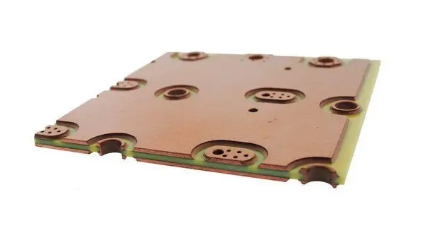
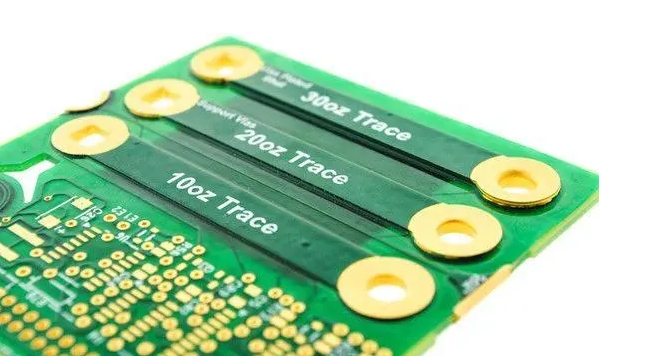
Heavy Copper Board does not have a set of definition per IPC. According to PCB industry, however, peopel generally use this name to identify a printed circuit board with copper conductors 3 oz/ft2 – 10 oz/ft2 in inner and/or outer layers. And Extreme heavy copper PCB refers to 20 oz/ft2 to 200 oz/ft2 printed circuit board.
Heavy copper normally used for a various products but not limited to: high power distribution, heat dissipation, planar transformers, power convertors, and so on.
Generally, the thick copper plate is about 3oz, and the larger current is 3oz~6oz. To achieve 15 ounces, the requirements for process and manufacturers are more stringent. Best provides 3-15oz 1-99 layers of PCB. It is a professional PCB manufacturer with 18 years of experience, providing one-stop PCB and PCBA services from design, manufacturing to after-sales.
Common copper foil thicknesses have the following options:
1 oz (35 μm): This is the most common and standard copper foil thickness, widely used in general electronic product manufacturing. It has good electrical and thermal conductivity.
2 oz (70 μm): This thickness of copper foil is usually used in circuits that require higher current carrying capacity, such as power amplifiers, high-power LEDs, etc.
0.5 oz (18 μm): This thinner copper foil thickness is suitable for some light and small electronic products, such as electronic watches, mobile phones, etc.
Other thicknesses: According to special needs, you can also choose copper foil of other thicknesses, such as 3 oz, 4 oz, etc.
What is copper foil
Copper foil is a cathodic electrolytic material, a thin, continuous metal foil deposited on the substrate layer of the circuit board, which serves as the conductor of the PCB. It is easy to adhere to the insulating layer, accept the printed protective layer, and form a circuit pattern after corrosion. The copper mirror test is a flux corrosion test, using a vacuum precipitation film on a glass plate. Copper foil is made of copper and a certain proportion of other metals. Copper foil generally has two types: 90 foil and 88 foil, that is, the copper content is 90% and 88%, and the size is 16*16cm.
How thick is the PCB copper foil
The commonly used international PCB copper foil thicknesses are: 35um, 50um, and 70um. Generally, the thickness of copper foil (copper cladding) of single-sided and double-sided PCB boards is about 35um (1.4mil), and the other specifications are 50um and 70um. The surface thickness of multilayer boards is generally 35um=1oz (1.4mil), and the inner layer is 17.5um (0.7mil). 70% of circuit boards use a copper foil thickness of 35um, which mainly depends on the purpose of the PCB and the voltage and current of the signal; in addition, for PCBs that need to pass large currents, some will use 70um copper thickness, 105um copper thickness, and rarely 140um, etc. The copper foil thickness is usually expressed in oz (ounces). 1oz refers to the thickness of 1oz of copper evenly covering an area of 1 square foot, which is about 1.4mil. It uses the weight per unit area to express the average thickness of the copper foil. Expressed in formula, that is, 1oz=28.35g/ FT2 (FT2 is square feet, 1 square foot = 0.09290304 square meters).
Different uses have different copper foil thicknesses,
Ordinary 0.5oz, 1oz
2oz, mostly used in consumer and communication products. Thick copper products above
3oz are mostly used for large currents, such as high-voltage products and power boards!
Copper foil thickness (track width) affects the current size. Although there is a formula that can directly calculate the current load capacity of copper foil, it is not so simple when actually designing the circuit. Therefore, safety should be fully considered when designing.
How thick is 2 oz of copper for PCB?
In the PCB industry, 1OZ means the thickness of 1OZ of copper evenly laid on an area of 1 square foot (FT2). It uses the weight per unit area to express the average thickness of the copper foil. Expressed in formula, 1OZ=28.35g/FT2 (FT2 is square feet, 1 square foot=0.09290304 square meters). First, we know that the density constant of copper and the conversion formula of related units are as follows: 1 cm = 10 mm; 1 mm = 1000 um 1 FT2≈929.0304cm2 According to the mass calculation formula m=ρ×V(volume)=ρ×S(area)×t(thickness), we know that the weight of copper foil divided by the density and area of copper is the thickness of copper foil! So, t=28.35÷929.0304÷8.9cm≈0.0034287cm=34.287um≈34.287÷25.4mil≈1.35mil Copper thickness 1.OZ(0.035mm) Copper thickness 1.5OZ(0.05mm) Copper thickness 2.OZ (0.07mm)
What are the materials of PCB board
FR-1——phenolic cotton paper, this base material is commonly known as bakelite (more economical than FR-2) FR-2——phenolic cotton paper FR-3——cotton paper, epoxy resin FR-4——glass cloth, epoxy resin FR-5——glass cloth, epoxy resin FR-6——matte glass, polyester G-10——glass cloth, epoxy resin CEM-1——cotton paper, epoxy resin (flame retardant) CEM-2——cotton paper, epoxy resin (non-flame retardant) CEM-3——glass cloth, epoxy resin CEM-4——glass cloth, epoxy resin CEM-5——glass cloth, polyester AIN——aluminum nitride SIC——silicon carbide
This website uses cookies to enhance your experience, remember your preferences, and help us understand how visitors use our site. You can accept all cookies, reject non-essential cookies, or manage your settings.
This website uses cookies to improve your experience while you navigate through the website. Out of these cookies, the cookies that are categorized as necessary are stored on your browser as they are essential for the working of basic functionalities of the website. We also use third-party cookies that help us analyze and understand how you use this website. These cookies will be stored in your browser only with your consent. You also have the option to opt-out of these cookies. But opting out of some of these cookies may have an effect on your browsing experience.
Necessary cookies are absolutely essential for the website to function properly. These cookies ensure basic functionalities and security features of the website, anonymously.
Cookie
Duration
Description
cookielawinfo-checkbox-analytics
11 months
This cookie is set by GDPR Cookie Consent plugin. The cookie is used to store the user consent for the cookies in the category "Analytics".
cookielawinfo-checkbox-functional
11 months
The cookie is set by GDPR cookie consent to record the user consent for the cookies in the category "Functional".
cookielawinfo-checkbox-necessary
11 months
This cookie is set by GDPR Cookie Consent plugin. The cookies is used to store the user consent for the cookies in the category "Necessary".
cookielawinfo-checkbox-others
11 months
This cookie is set by GDPR Cookie Consent plugin. The cookie is used to store the user consent for the cookies in the category "Other.
cookielawinfo-checkbox-performance
11 months
This cookie is set by GDPR Cookie Consent plugin. The cookie is used to store the user consent for the cookies in the category "Performance".
viewed_cookie_policy
11 months
The cookie is set by the GDPR Cookie Consent plugin and is used to store whether or not user has consented to the use of cookies. It does not store any personal data.
Functional cookies help to perform certain functionalities like sharing the content of the website on social media platforms, collect feedbacks, and other third-party features.
Performance cookies are used to understand and analyze the key performance indexes of the website which helps in delivering a better user experience for the visitors.
Analytical cookies are used to understand how visitors interact with the website. These cookies help provide information on metrics the number of visitors, bounce rate, traffic source, etc.
Advertisement cookies are used to provide visitors with relevant ads and marketing campaigns. These cookies track visitors across websites and collect information to provide customized ads.