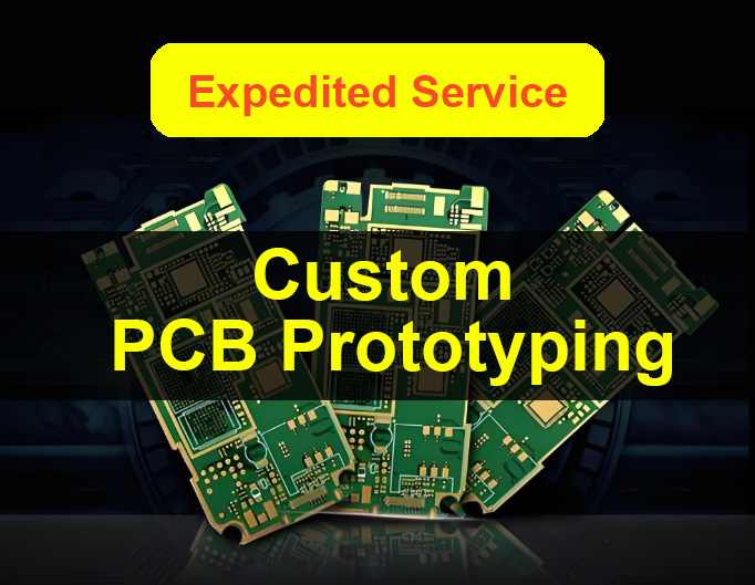
Best PCB manufacturers in China represent a group of leading electronics manufacturing service (EMS) providers renowned for combining advanced technological capabilities with cost-effectiveness. This comprehensive guide will explore the key players, selection criteria, and technical strengths that define the top-tier PCB supply chain in China, with a specific focus on full-turnkey services from design to box build.
Are you struggling to navigate the vast landscape of PCB production in China, worried about quality consistency, communication barriers, or finding a partner that can handle complex projects like HDI PCBs from design to box build?
- Uncertain Quality: Fear of receiving substandard boards that fail in testing or have a short lifespan.
- Communication Challenges: Time zone differences and language barriers leading to misunderstandings and project delays.
- Limited Technical Scope: Finding a manufacturer that only does fabrication, forcing you to manage assembly separately.
- Inconsistent Pricing: Hidden costs and fluctuating quotes that blow the project budget.
- Long Lead Times: Slow production and shipping timelines that impact your product’s time-to-market.
The good news is that these common challenges have clear solutions when you partner with best PCB manufacturers in China.
- Stringent Quality Control: Implementation of rigorous quality management systems (like ISO 9001, IATF 16949) and multiple inspection points throughout production.
- Dedicated Customer Support: Assigning experienced project managers who provide clear, proactive communication in English.
- Full Turnkey Services: Offering an integrated solution that includes PCB fabrication, component sourcing, PCB assembly, and final box-build assembly.
- Transparent Quoting: Providing detailed, upfront quotes with no hidden fees, often with cost-saving design for manufacturability (DFM) advice.
- Optimized Production Flow: Utilizing advanced equipment and streamlined processes to guarantee fast PCB manufacturing without sacrificing quality.
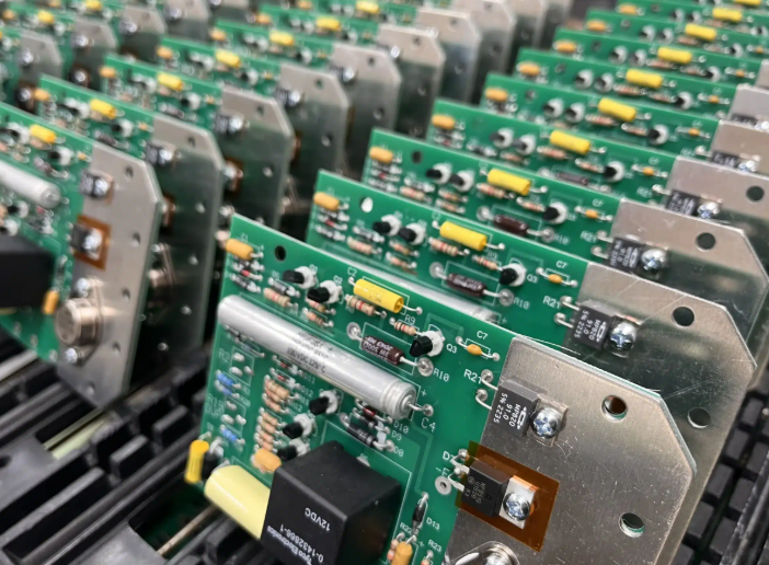
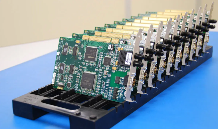
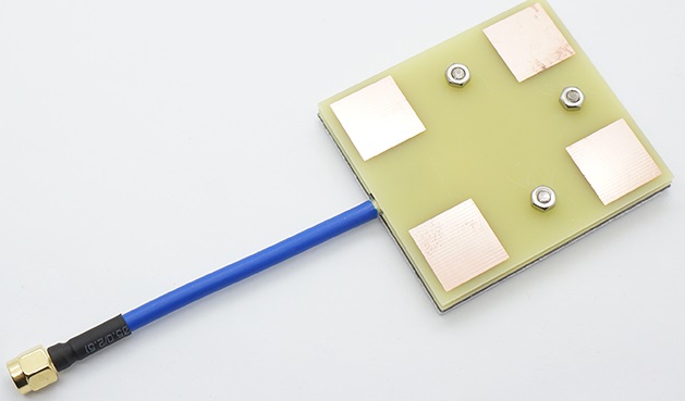
Among the PCB manufacturers in China, BEST Technology stands out as a premier partner. We are a professional PCB and EMS factory with over 19 years of experience, specializing in providing end-to-end solutions from design and prototyping to mass production and box-build assembly. Our commitment to quality, advanced technical capabilities in areas like HDI PCB, high speed board, RF printed circuit board, copper MCPCB, star MCPCB, ceramic base PCB, and exceptional customer service make us a trusted choice for global clients. For inquiries, pls feel free to contact us at sales@bestpcbs.com.
What Factors Define the Best PCB Manufacturers in China?
Selecting the right partner goes beyond just comparing prices. The best PCB manufacturers in China are distinguished by a combination of capabilities, certifications, and services that ensure reliability and value.
- Comprehensive Service Range: The top manufacturers offer a complete “Design to Box Build” service.
This includes PCB layout support, PCB fabrication, component procurement, PCB manufacturing and assembly, testing, and final product integration.
This simplifies the supply chain and ensures accountability at every stage.
- Technical Proficiency and Specialization: Look for manufacturers with expertise in the specific technologies you need.
This includes capabilities for standard boards, as well as advanced processes for HDI PCB, high-frequency boards, heavy copper, and flexible circuits.
Their technical depth directly impacts your product’s performance.
- Robust Quality Assurance Systems: Certifications like ISO 9001, ISO 13485, IATF 16949, AS9100D are baseline indicators.
The best manufacturers have in-house testing labs (for ICT, Flying Probe, X-Ray, etc.) and a proven track record of high yield rates.
- Transparent Communication and Project Management: Effective communication is critical.
The leading providers assign a dedicated project manager to act as a single point of contact, providing regular updates and swiftly addressing any concerns.
- Proven Experience and Reputation: A long history of successful projects, especially with international clients, is a strong positive signal.
Client testimonials and case studies offer valuable insights into their reliability and performance.
In summary, the best manufacturers are those that provide a seamless, high-quality, and transparent partnership, mitigating the risks typically associated with overseas production.
Is BEST Technology a PCB Manufacturer in China?
Yes, absolutely. BEST Technology is a established and well-regarded PCB manufacturer in China.
- We operate our own modern manufacturing facilities equipped for both standard and advanced PCB fabrication.
- Our services extend far beyond simple board production; we are a full-scale EMS provider.
- This means we manage the entire process, from sourcing raw materials and components to PCB manufacturing and assembly, and finally, assembling the finished product into its enclosure (box build).
- Our integrated approach ensures greater control over quality, cost, and scheduling, making us a true one-stop-shop for our clients.
Top 10 Best PCB Manufacturers in China
While rankings can vary, the following list represents some of the most prominent and capable PCB manufacturers in China, known for their scale, quality, and service offerings. This China PCB manufacturer list includes:
- BEST Technology: Distinguished by our strong focus on engineering support and full turnkey PCB manufacturing and assembly services, especially for complex projects requiring HDI PCB, PCBA and reliable box-build assembly.
- PCBWay: A major player in the prototype and small-batch market, offering a wide range of capabilities and an active online community.
- Kingboard Holdings: One of the largest PCB manufacturer in the world, supplying a massive volume of boards to various industries.
- Shennan Circuits Co., Ltd. (SCC): A leading manufacturer focusing on high-end, high-layer count boards for communications and servers.
- AT&S: A global high-end PCB supplier with significant production bases in China, specializing in HDI and substrate-like PCBs.
- WUS Printed Circuit Co., Ltd.: A major manufacturer with strong capabilities in automotive and communication PCBs.
- Kinwong Electronic: A large-scale producer with a strong presence in automotive, consumer electronics, and data storage.
- JLC PCB (Shenzhen JLC Electronics Co., Ltd.): Best known for its incredibly user-friendly online platform and low-cost, quick-turn prototypes.
- Tripod Technology Corporation: A top-tier global manufacturer with extensive facilities in China, producing a wide range of PCB types.
- Compeq Manufacturing Co., Ltd.: A major supplier of HDI, flexible, and rigid-flex PCBs for smartphones and consumer devices.
This top 10 PCB manufacturers in china list showcases the diversity of the market, from giants focused on volume to specialized partners like BEST Technology that excel in comprehensive service.
How to Choose Between Top PCB Manufacturers in China and the Best PCB Manufacturers in USA?
The choice between a Chinese and a US-based manufacturer involves a trade-off between several key factors.
- Cost: This is the most significant advantage for Chinese manufacturers.
Lower labor and overhead costs typically result in substantially lower prices, especially for medium to high-volume production. - Lead Time and Logistics: Best PCB manufacturers in USA offer shorter shipping times and can be advantageous for rapid iterations or projects with very tight timelines.
However, many Chinese manufacturers have optimized their processes for Fast PCB manufacturing and offer expedited shipping options. - Communication and IP Protection: US-based manufacturers have no language barrier and operate under US intellectual property laws, which some companies prefer.
Reputable Chinese manufacturers like BEST Technology have English-speaking teams and strict NDAs to protect client IP. - Technical Capability: Both regions have highly capable manufacturers.
China’s ecosystem is vast, with many specialists in advanced technologies like HDI PCB.
The choice often comes down to the specific technical requirements of the project.
Overall, for projects where cost-efficiency is paramount and volumes are medium to high, the best PCB manufacturers in China are typically the superior choice, especially when you partner with a reliable provider that mitigates concerns about communication and quality.
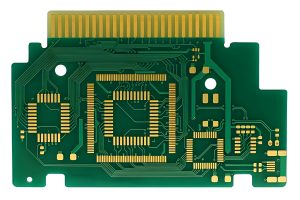
What are the Technical Capabilities of the Manufacturer of HDI PCB in China?
When you work with the manufacturer of HDI PCB in China, such as BEST Technology, you are essentially partnering with a factory built around high-density, high-precision interconnect technology—not just standard multilayer boards. Our capabilities cover the full chain from via structure design to complex stack-ups, materials, and final finishing.
Below is a consolidated view of our main technical strengths, based on real HDI manufacturing capabilities at BEST Technology.
1. Full Range of HDI Via Structures
We design and manufacture all the core via types used in HDI PCB:
- Blind vias – connecting outer layers to one or more inner layers without passing through the whole board.
- Buried vias – connecting only internal layers, invisible from outside.
- Through-hole vias – standard plated through holes for robust interconnection and mechanical support.
For HDI, we distinguish clearly between:
Laser microvias (HDI vias)
- Laser-drilled diameter down to 0.07mm (70µm) for prototypes.
- Standard production microvia diameter around 0.10mm.
- Dielectric-to-hole aspect ratio controlled at about 1:1 to maintain plating stability.
- Use of RCC or laser-drillable prepregs for consistent microvia quality.
Mechanical blind/buried vias
- Hole diameters typically ≥0.20mm.
- A cost-effective choice when extreme density is not required.
2. Advanced Laser Drilling and Microvia Technology
We use advanced UV and CO₂ laser systems optimized for different copper thicknesses and dielectric stacks.
Key capabilities include:
Microvia diameter capability
- As small as 0.07mm for prototype builds
- Stable 0.10mm in mass production
Aspect ratio control
- Laser drill depth-to-diameter managed around 1:1, avoiding voids and improving plating uniformity
Material-specific drilling recipes
- Detailed drilling parameters defined according to copper weight and PP thickness
- With PP ≤70µm, we can directly drill very small microvias with excellent wall quality and adhesion
3. High-Layer-Count and Sequential Lamination Capability
To support complex HDI designs, we routinely perform multi-stage lamination with tight dimensional control.
Typical HDI structures we support
- 1+N+1
- 2+N+2 (stacked or staggered microvias)
- 3+N+3 and any-layer HDI
Layer count capability
- Up to 50 layers in standard production
- Up to 100 layers in advanced prototype builds (after technical review)
These capabilities enable routing for dense BGAs, FPGAs, ASICs, and high-speed differential pairs in compact layouts.
4. Fine Line / Space and Registration Accuracy
High-density interconnect designs require fine traces and accurate registration.
Line / space capability
- Inner layers: 2.5 / 2.5 mil
- Outer layers: 3 / 3 mil (finer options depending on copper weight)
Registration accuracy
- Maintained within ≤0.13mm layer-to-layer
This stability is essential for stacked microvias, via-in-pad designs, and fine-pitch BGA breakout (≤0.3mm pitch).
5. Comprehensive Material Expertise
We work with a wide variety of materials to support performance, thermal stability, and reliability:
Standard & High-Tg FR-4
- From standard Tg to ~180°C High-Tg
- High-CTI insulation options
High-speed / low-loss laminates
- Rogers
- Isola
- Taconic
- Arlon
(Suitable for RF, 5G, high-speed digital, impedance-controlled systems)
Thin-core HDI capability
- Minimum inner core thickness 0.05mm
- Enables compact, multi-stack HDI structures
This material flexibility allows us to optimize stack-ups for signal integrity, thermal performance, and cost.
6. Surface Finishes Optimized for HDI and Fine Pitch
We offer a full portfolio of finishes for fine-pitch and wire-bonding applications:
- ENIG
- ENEPIG
- Immersion Silver
- OSP
- Hard/soft gold plating
These finishes allow us to support:
- BGA pads as small as 8 mil
- Strong solderability and reliable wire-bonding performance
7. Board and Copper Thickness Range
We support a wide range of board constructions, from ultra-thin modules to power-dense designs.
Board thickness range
- As thin as 0.15mm
- Up to 10mm for heavy or high-power boards
Copper thickness range
- From ½ oz for fine-line HDI inner layers
- Up to 20 oz (inner layers) and 28 oz (outer layers) in special prototype builds
This allows us to support logic-dense HDI circuits and high-current power systems within the same manufacturing framework.
8. Robust Process Control and High Reliability
Our HDI capability is reinforced by strict process controls:
- Microvia plating:
- Copper thickness inside microvias controlled at ≥15µm for thermal-cycle reliability
- In-process inspection:
- Multiple AOI steps
- X-ray for internal registration and BGA solder inspection
- Impedance verification for high-speed designs
- 100% Electrical Testing:
- Flying Probe or fixture testing ensures no opens or shorts in the full HDI network
In brief, as the manufacturer of HDI PCB in China, we combine:
- Precision laser microvia drilling
- Multi-stage HDI stack-ups
- Fine line/space and registration control
- High-layer-count fabrication
- Material and surface finish expertise
- Wide board and copper thickness options
- And rigorous quality and reliability control
These strengths allow us to deliver HDI PCBs that are smaller, denser, and more powerful than conventional multilayer boards—giving your next-generation electronic products a strong technical foundation.
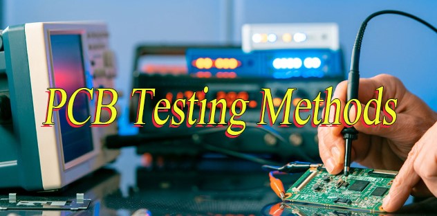
How Does the Best Manufacturer of PCB in China Ensure Quality?
The best manufacturer of PCB in China ensures quality through a multi-layered, system-wide approach that permeates every aspect of production. At BEST Technology, our philosophy is “Quality Built-In, Not Inspected In.”
- DFM Analysis: Before production begins, our engineers perform a thorough Design for Manufacturability analysis to identify and correct potential issues in the design file.
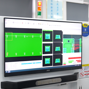
- In-Process Testing: Throughout PCB fabrication and assembly, boards undergo multiple inspections, including Automated Optical Inspection (AOI) to check for defects and X-Ray inspection to verify internal layer integrity and BGA soldering.
- Final Electrical Testing: 100% electrical testing (Flying Probe or Bed-of-Nails) is conducted to ensure the board’s circuitry matches the original design and is free of shorts or opens.
- Quality Management System: We adhere to strict international standards (ISO 9001, IATF 16949), which provide a framework for consistent processes, continuous improvement, and traceability.
- Material Control: We partner with reputable suppliers for raw materials (laminates, copper clad) and components, ensuring that every input meets our high standards.
Why Choose EBest Circuit (Best Technology) for Your Best PCB Manufacturer in China?
Choosing BEST Technology means selecting a partner dedicated to your project’s success from concept to completion. Here’s why we are a strong candidate for your best PCB manufacturer in China:
- End-to-End Solution: We provide a true “Design to Box Build” service, eliminating the hassle of managing multiple vendors.
- Engineering Expertise: Our team offers valuable DFM advice and specializes in complex technologies, including HDI PCB.
- Commitment to Quality: Our rigorous QC processes guarantee that you receive reliable, high-performance boards.
- Transparent Partnership: We believe in clear communication and honest pricing, building long-term relationships with our clients.
- Agile and Responsive: Whether you need a quick-turn prototype or Fast PCB manufacturing for mass production, we adapt to your timeline.
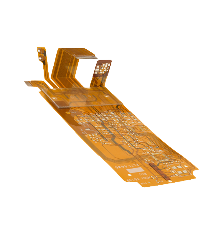
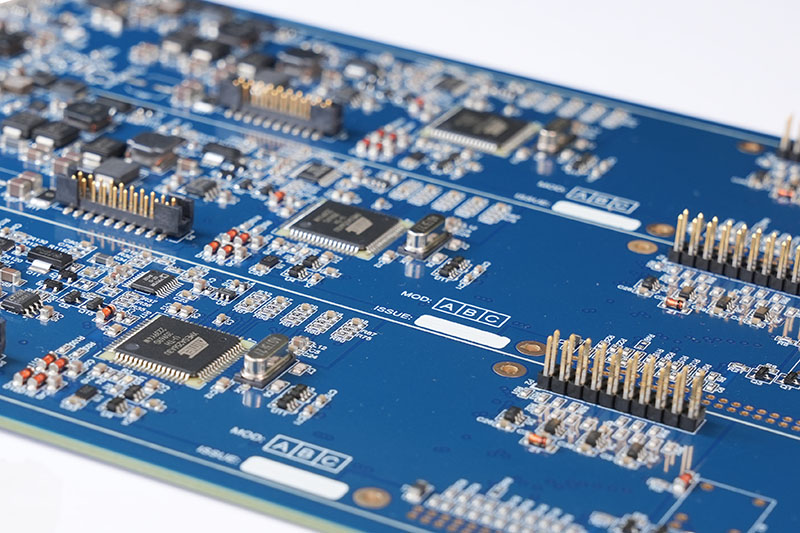
Case of HDI PCB Manufacturing and Assembly by EBest Circuit (Best Technology)
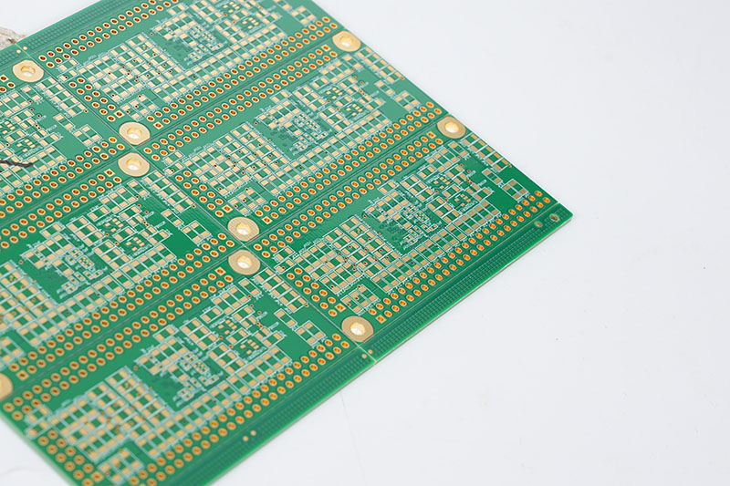
This case study examines the manufacturing of a sophisticated 8-layer, 3-stage HDI PCB by EBest Circuit (Best Technology). This board exemplifies the advanced capabilities required for modern, high-performance electronic devices where miniaturization, reliability, and signal integrity are paramount. The following sections detail its diverse application scenarios and key technical parameters.
The technical specifications of this PCB make it suitable for a wide range of demanding applications across several industries:
- Advanced Medical Imaging Systems: This board is ideal for portable ultrasound machines, handheld diagnostic devices, and high-resolution patient monitoring equipment. The 3 step HDI technology allows for the dense integration of high-speed processing chips necessary for real-time image rendering and data analysis, while the high-TG180 material ensures stability during repeated sterilization cycles and reliable operation in critical healthcare environments.
- Next-Generation Automotive ADAS and LiDAR Modules: In the automotive sector, this PCB can serve as the main processing unit for Advanced Driver-Assistance Systems (ADAS), LiDAR sensors, and autonomous vehicle control modules. Its robust construction (1oz copper, 1.6mm thickness) provides durability against vibration and thermal stress, and the high-density interconnects are essential for handling the massive data flow from multiple cameras and sensors, enabling faster and safer decision-making.
- High-Frequency Telecommunications and Networking Equipment: This board is perfectly suited for core routers, network switches, and 5G baseband units. The combination of 3 step HDI and controlled impedance design supports high-speed data transmission with minimal signal loss. The ENIG surface finish offers excellent planarity for reliable soldering of fine-pitch BGAs found on modern FPGAs and ASICs, ensuring uninterrupted performance in telecommunications infrastructure.
PCB Technical Parameters
- Layer Count and Type: 8 Layers
- Base Material: FR4, High TG180
- Copper Weight (Inner/Outer): 1oz / 1oz
- Solder Mask Color: Green
- Silkscreen Color: White
- Final Board Thickness: 1.6mm
- HDI Technology: 3-Stage HDI
- Via Filling: Resin Filled
- Surface Finish: ENIG (1u” Gold)
To wrap up, Best PCB manufacturers in China are defined by their ability to deliver high-quality, cost-effective, and comprehensive manufacturing solutions for a global market. This guide has outlined the critical factors, key players, and technical competencies that set the leading providers apart.
For businesses seeking a reliable partner that combines technical expertise in areas like HDI PCB with a full turnkey “Design to Box Build” service model, BEST Technology offers an compelling solution. Our focus on quality assurance, transparent communication, and engineering support ensures your project is in capable hands. A warm welcome to contact our team at sales@bestpcbs.com for a prompt and professional consultation.