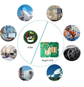
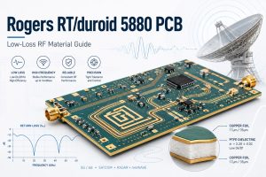
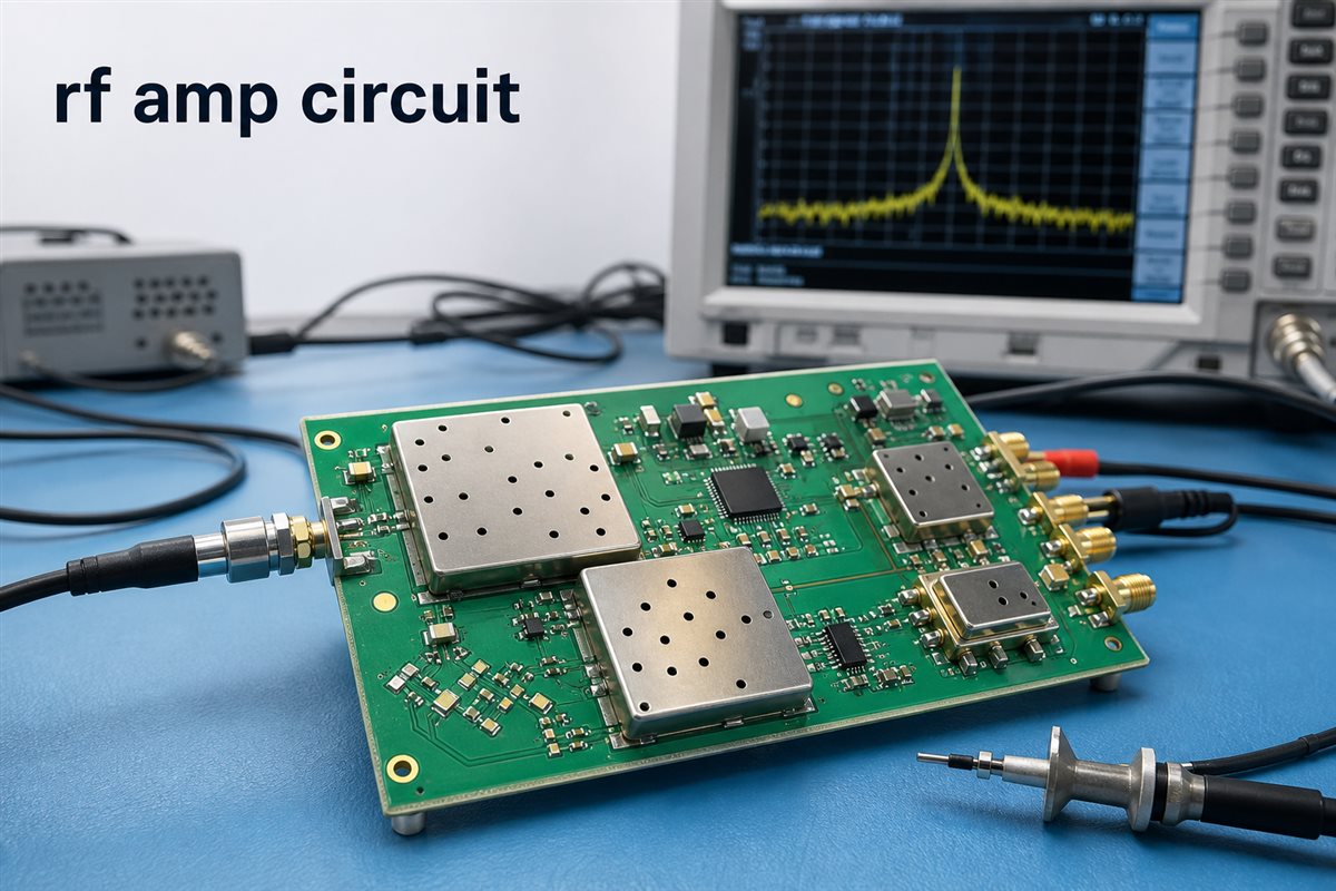
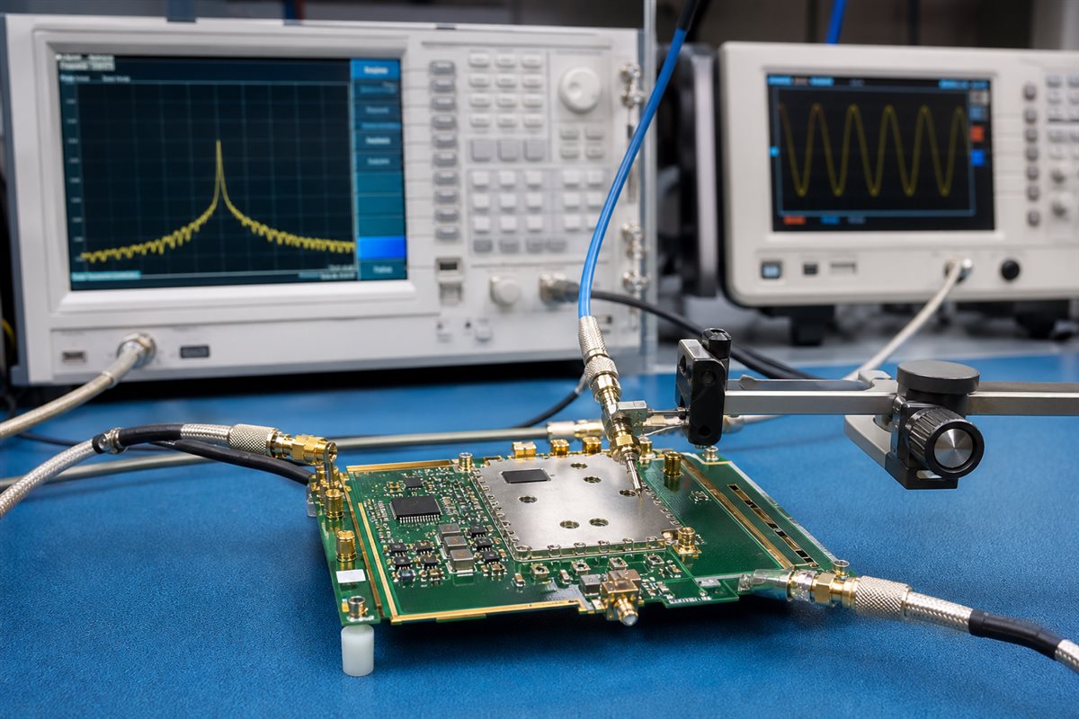
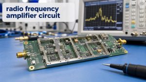
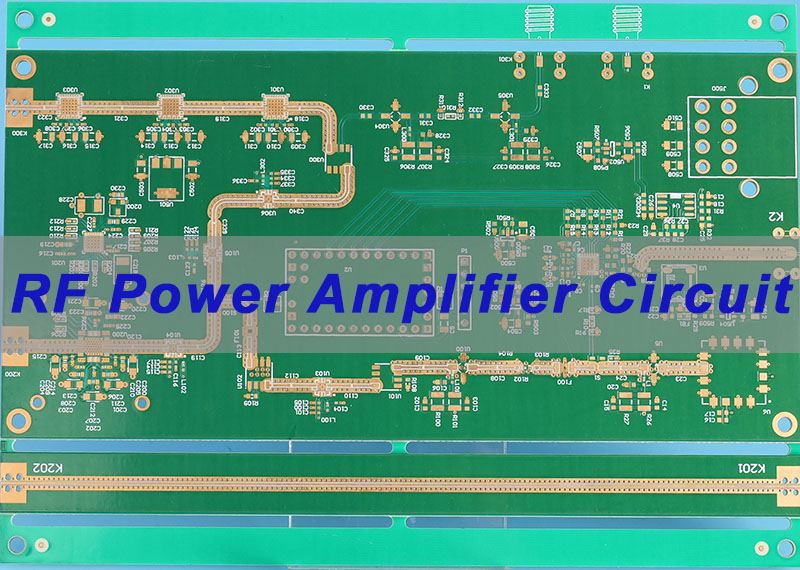
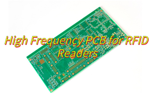
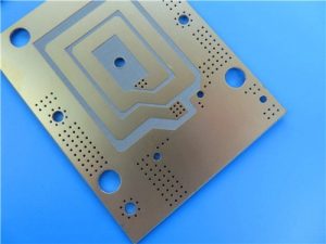
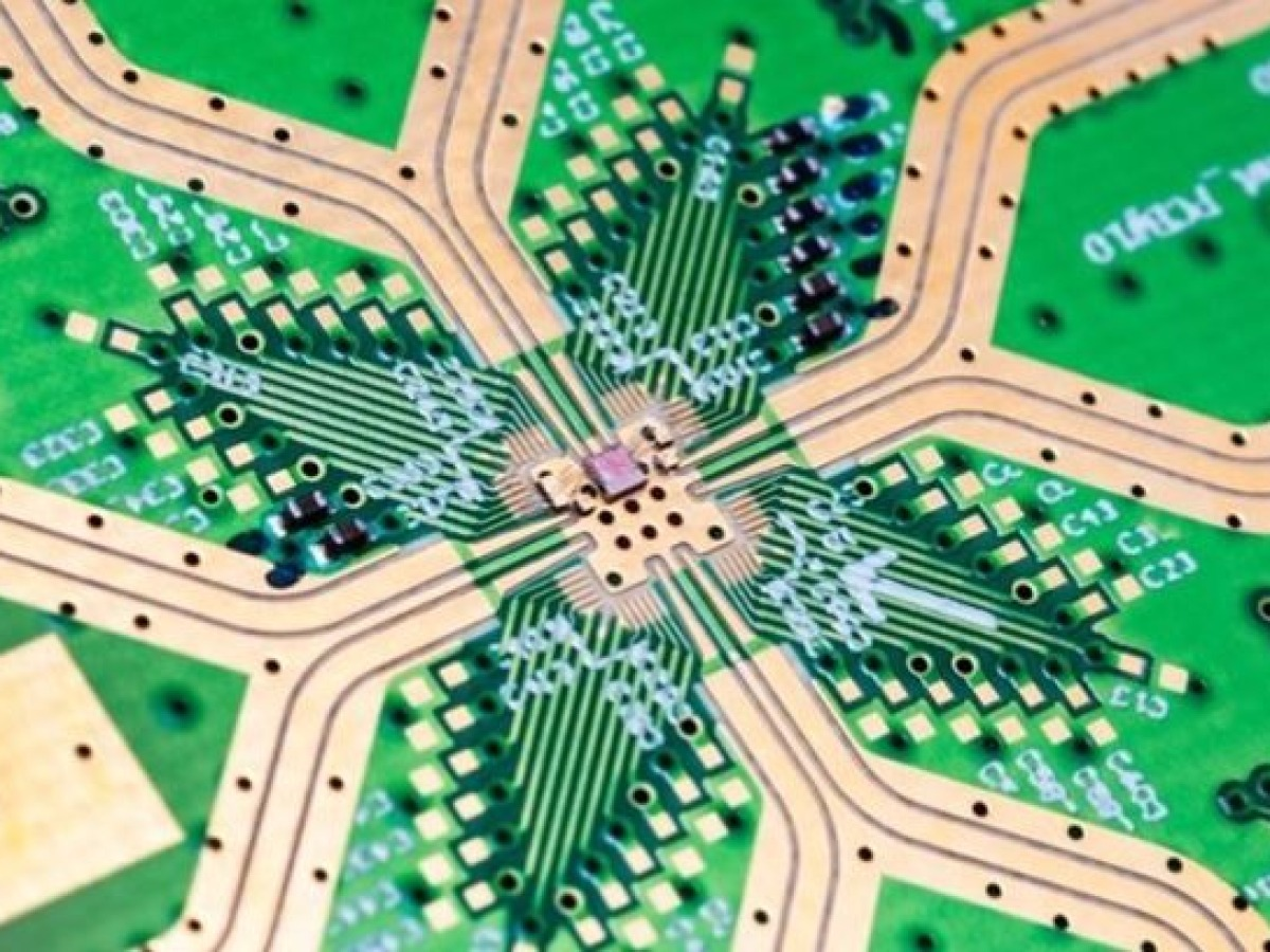
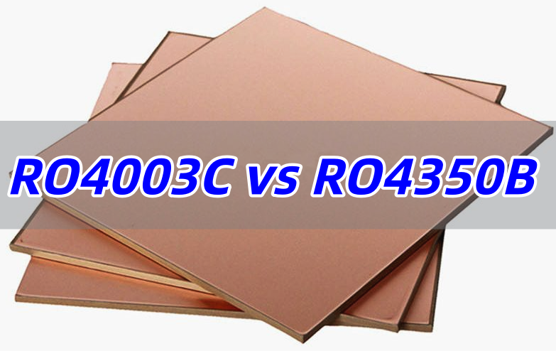
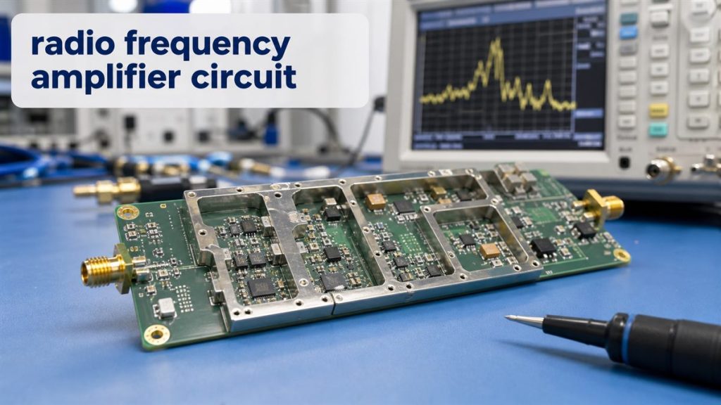
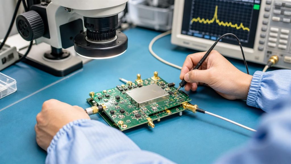
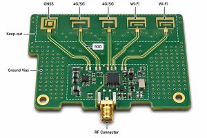
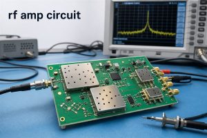
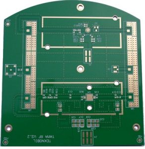
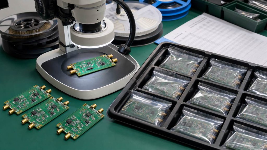
A Rogers PCB is usually considered when standard FR4 can no longer meet the electrical requirements of an RF, microwave, antenna, radar, or other frequency-sensitive circuit. Compared with general-purpose FR4, Rogers laminates such as RO4003C, RO4350B and RT/duroid 5880 offer lower dielectric loss and more tightly controlled dielectric properties for high-frequency designs.
EBest Circuit is a PCB and PCBA manufacturer with over 20 years of experience, with manufacturing facilities in China and Vietnam. We support Rogers PCB fabrication, Rogers/FR4 hybrid boards, controlled-impedance PCBs, and PCB assembly for high-frequency projects. Our RF PCBs are used in microwave systems, radar, IoT communication, wireless equipment, Wi-Fi devices, and antenna applications. If you have a similar RF PCB project, contact us with your Gerber files and specifications for engineering review and quotation.
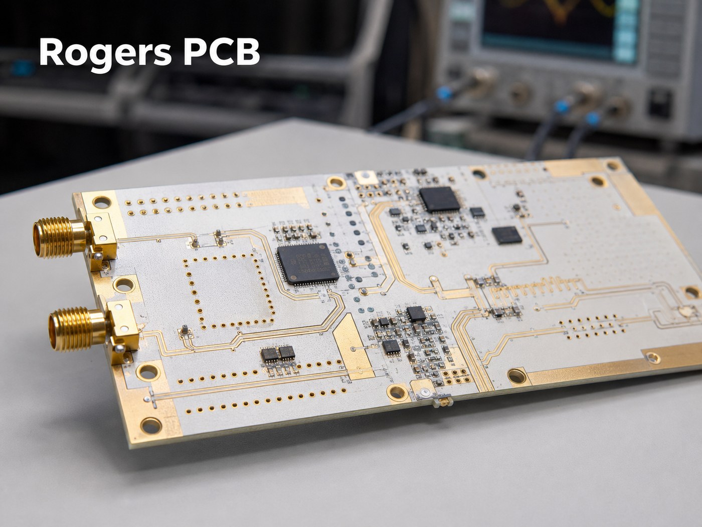
What Is a Rogers PCB?
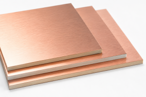
A Rogers PCB is a printed circuit board that uses one or more high-frequency laminates supplied by Rogers Corporation.
Common constructions include:
- Two-layer RF boards
- Four-layer controlled-impedance PCBs
- Multilayer Rogers PCBs
- Rogers/FR4 hybrid PCBs
- PTFE microwave boards
The key point is that Rogers is a material brand rather than one fixed PCB substrate.
RO4003C and RO4350B belong to the hydrocarbon/ceramic RO4000 family. RO3003 is a ceramic-filled PTFE laminate, while RT/duroid 5880 is based on PTFE reinforced with glass microfibers.
Why Are Rogers Materials Used for High-Frequency PCBs?
At higher frequencies, the laminate becomes part of the transmission structure. Its electrical properties directly influence impedance, signal loss, wavelength, and phase.
The main parameters engineers consider are:
| Parameter | Effect on PCB Performance |
|---|---|
| Dielectric constant, Dk | Impedance, trace width, wavelength, phase |
| Dissipation factor, Df | Dielectric loss and insertion loss |
| Dk stability | Impedance and phase consistency |
| Copper profile | Conductor loss at high frequencies |
| Dimensional stability | RF geometry and multilayer registration |
| Thermal behavior | Electrical stability over temperature |
Rogers materials are selected mainly because these properties are more tightly characterized for RF and microwave use than those of typical general-purpose FR4.
What Rogers PCB Materials Are Commonly Used?
Several Rogers laminate families are available, but four materials are especially common in RF and microwave designs.
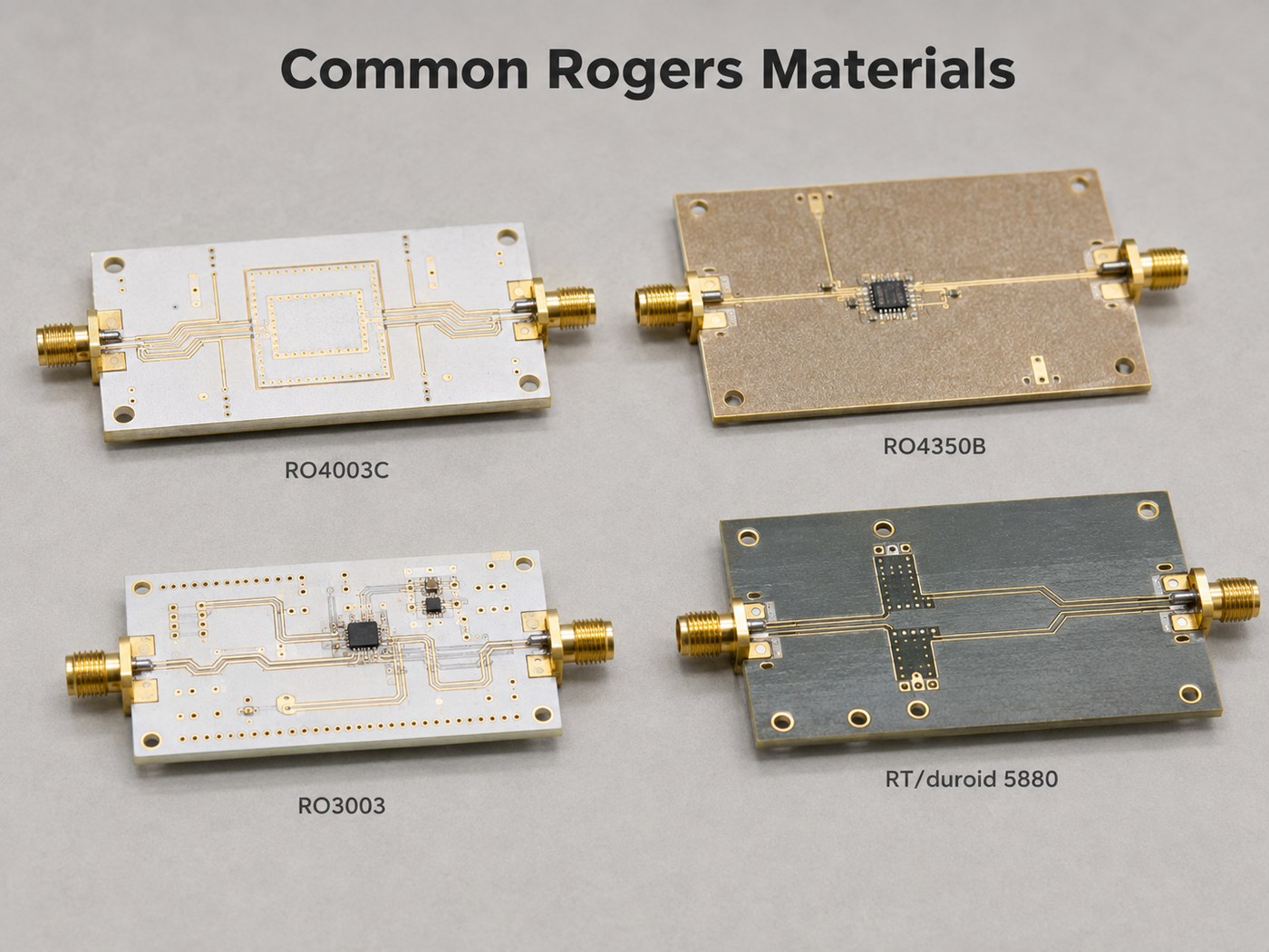
| Rogers Material | Material System | Process Dk | Df at 10 GHz | Typical Applications |
|---|---|---|---|---|
| RO4003C | Hydrocarbon/ceramic | 3.38 ±0.05 | 0.0027 | RF circuits, antennas, microwave boards |
| RO4350B | Hydrocarbon/ceramic | 3.48 ±0.05 | 0.0037 | RF multilayers, telecom, industrial RF |
| RO3003 | Ceramic-filled PTFE | 3.00 ±0.04 | 0.0010 | Radar, mmWave, phase-sensitive circuits |
| RT/duroid 5880 | PTFE/glass microfiber | 2.20 ±0.02 | 0.0009 | Very low-loss microwave and broadband RF |
RO4003C is commonly chosen when a circuit needs lower loss and more predictable dielectric behavior than standard FR4 while keeping fabrication relatively straightforward.
RO4350B serves a similar RF range and is UL 94 V-0 rated, which can be useful when flame-rating requirements apply.
RO3003 is suited to microwave and mmWave applications where stable dielectric behavior is important, including radar and antenna circuits.
RT/duroid 5880 is often used where very low transmission loss is a primary design requirement.
Rogers PCB vs FR4: What Is the Difference?
The main difference is not simply that Rogers is “better.” The real question is whether the electrical performance of the selected FR4 laminate is sufficient for the design.
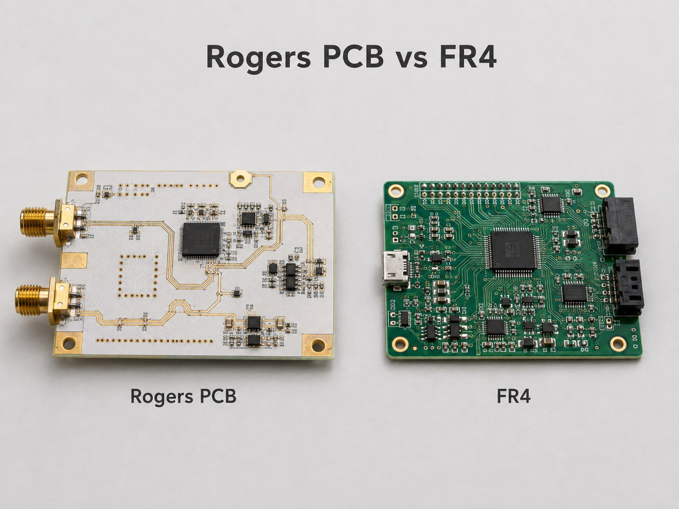
| Factor | Rogers High-Frequency Material | Conventional FR4 |
|---|---|---|
| Dielectric properties | More tightly controlled for RF | Depends on laminate grade |
| Dielectric loss | Low to very low | Generally higher |
| RF impedance stability | Better suited to sensitive RF structures | Usually adequate for less demanding circuits |
| Material options | Multiple RF/microwave families | Broad general-purpose range |
| Fabrication | Varies by Rogers material family | Highly standardized |
| Cost | Higher | Lower |
| Typical use | RF, microwave, radar, antennas | Digital, control, power, general electronics |
FR4 is still appropriate for many lower-frequency and less loss-sensitive circuits. Rogers materials become more valuable when insertion loss, impedance tolerance, or phase stability is difficult to maintain with the selected FR4 system.
A Rogers/FR4 hybrid PCB can also be used when only the RF portion of the board requires a high-frequency laminate.
How Do You Choose the Right Rogers PCB Material?
Start with the electrical specification rather than selecting a laminate only by product name.
| Selection Factor | What to Define |
|---|---|
| Operating frequency | Frequency range of the circuit |
| Insertion loss | Maximum acceptable RF or channel loss |
| Impedance | Target impedance and tolerance |
| Phase requirement | Allowable phase or electrical-length variation |
| Temperature range | Minimum and maximum operating temperature |
| Layer count | Total layers and RF layer position |
| Dielectric thickness | Distance between signal and reference plane |
| Copper weight | Copper thickness on critical layers |
| Flame rating | Required safety classification |
| Budget | Prototype and production cost target |
A 2.4 GHz wireless board and a 77 GHz radar PCB, for example, can require very different laminate properties even though both are considered RF designs.
Material choice should therefore match the actual frequency, loss, and impedance requirements of the circuit.
What Rogers PCB Thicknesses Are Available?
Rogers PCB thickness usually refers to either dielectric thickness or finished board thickness. These are not the same.
The dielectric thickness is the distance between the RF trace and its reference plane, so it directly affects controlled impedance. Finished PCB thickness is determined by the complete stackup, including cores, bonding materials, copper, and plating.
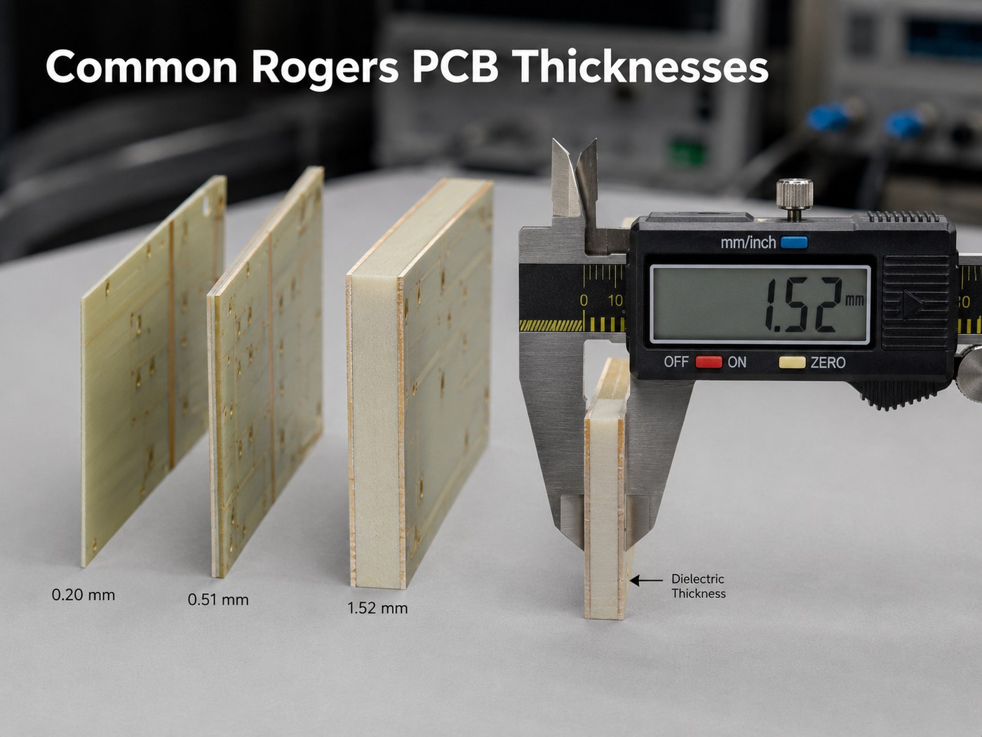
Common Rogers PCB Thicknesses
The values below are common dielectric thicknesses rather than finished board thicknesses.
| Rogers Material | Common Dielectric Thicknesses |
|---|---|
| RO4003C | 0.20, 0.30, 0.41, 0.51, 0.81, 1.52 mm |
| RO4350B | 0.17, 0.25, 0.51, 0.76, 1.52 mm |
| RO3003 | 0.13, 0.25, 0.51, 0.76, 1.52 mm |
| RT/duroid 5880 | 0.13, 0.25, 0.51, 0.79, 1.57 mm |
For an impedance-controlled RFQ, specify the Rogers material grade, dielectric thickness, finished PCB thickness, copper weight, and target impedance rather than only requesting a “1.6 mm Rogers PCB.”
How Is a Multilayer or 4-Layer Rogers PCB Stackup Designed?
A four-layer Rogers PCB can use Rogers material throughout the stackup or combine Rogers and FR4 in a hybrid structure.
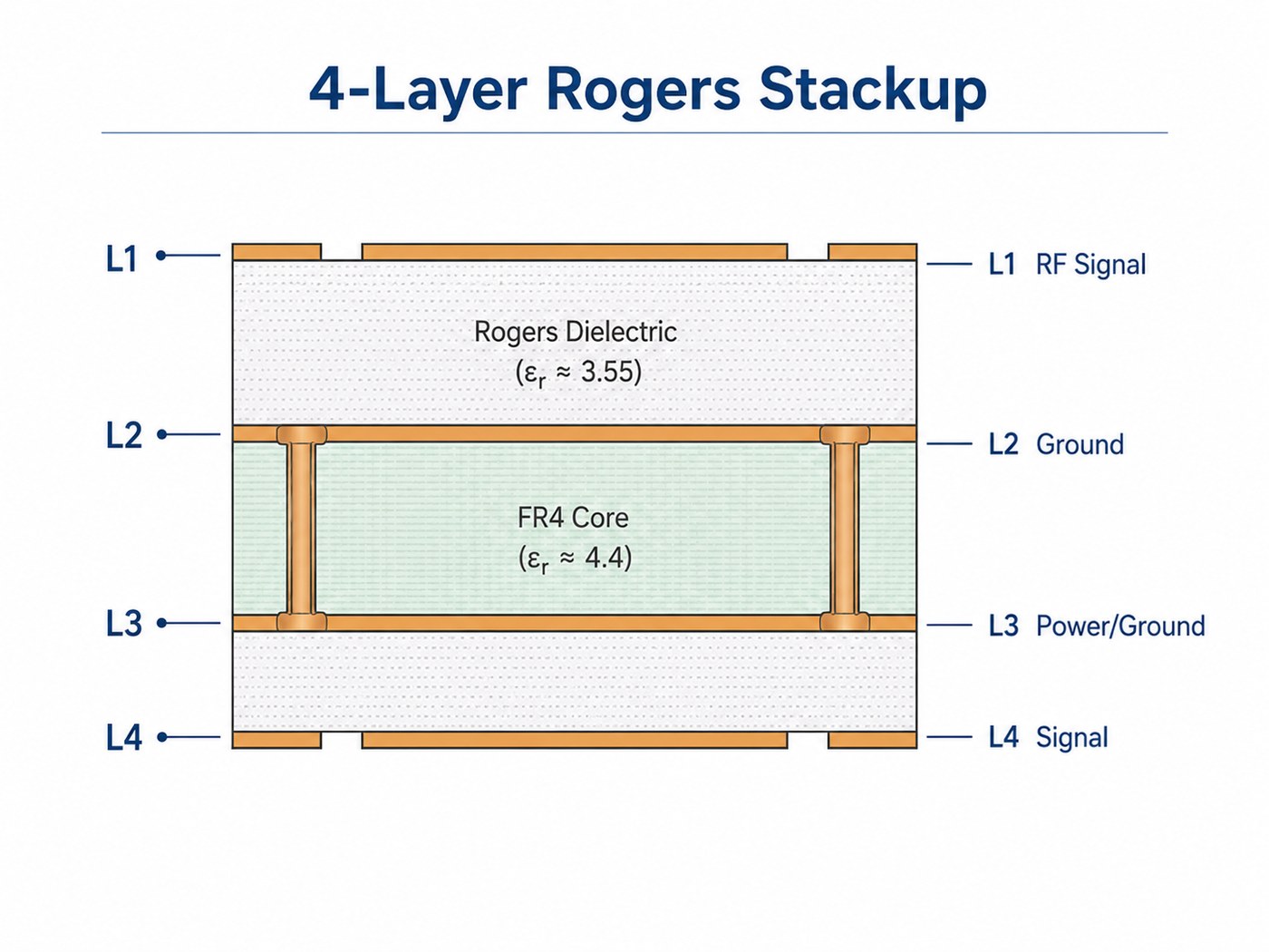
A simple all-Rogers example may be:
| Layer | Function |
|---|---|
| L1 | RF signal and components |
| Rogers dielectric | RF dielectric |
| L2 | Ground |
| Rogers bonding/core structure | Interlayer dielectric |
| L3 | Power or reference |
| Rogers dielectric | Dielectric |
| L4 | Signal |
A hybrid construction may use Rogers only around the critical RF layer:
| Layer | Function |
|---|---|
| L1 | RF signal |
| Rogers laminate | Controlled RF dielectric |
| L2 | RF ground |
| FR4 structure | General-purpose dielectric |
| L3 | Power or ground |
| FR4 | General-purpose dielectric |
| L4 | Digital or control signal |
Hybrid stackups can reduce material cost, but the PCB manufacturer still needs to review bonding materials, CTE behavior, total thickness, and lamination compatibility.
For controlled-impedance designs, the stackup should be confirmed before the final RF trace width is locked.
What Should You Consider When Designing a Rogers PCB?
Rogers PCB design should be based on the actual laminate and production stackup.
Key design checks include:
- Controlled impedance
- Dielectric thickness
- Dk used for modeling
- Copper thickness
- Copper foil roughness
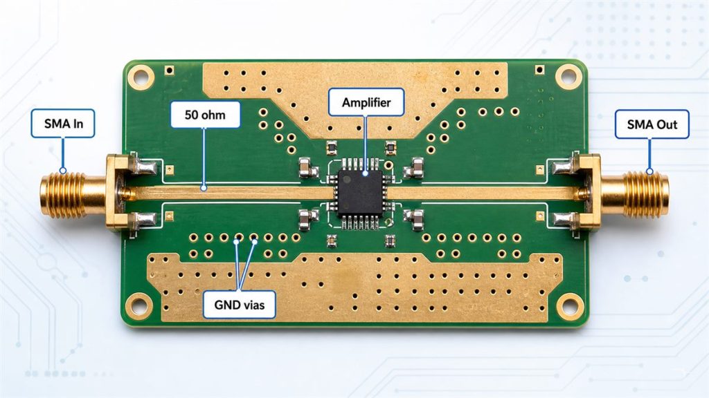
- Ground-plane continuity
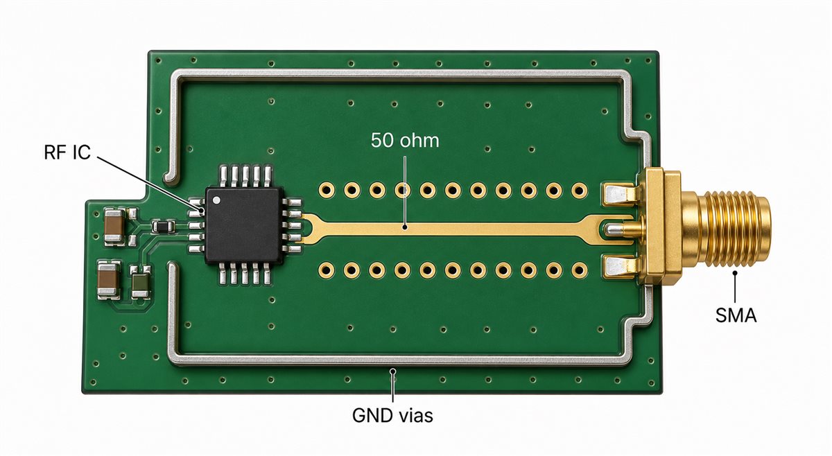
- Via fencing
- Return-current paths
- Connector launches
- Layer transitions
- Via stubs
- RF trace-to-edge clearance
- Etching tolerance
- Surface finish
- Solder mask over critical RF traces
One common design issue is the use of the wrong Dk value.
Process Dk vs Design Dk
| Material | Process Dk | Typical Design Dk |
|---|---|---|
| RO4003C | 3.38 | 3.55 |
| RO4350B | 3.48 | 3.66 |
Process Dk and Design Dk are used for different purposes, so the appropriate value should be selected according to the transmission-line model and design method.
For controlled-impedance fabrication, provide the manufacturer with the target impedance, laminate grade, dielectric thickness, copper requirement, and RF layer information.
How Is a Rogers PCB Manufactured?
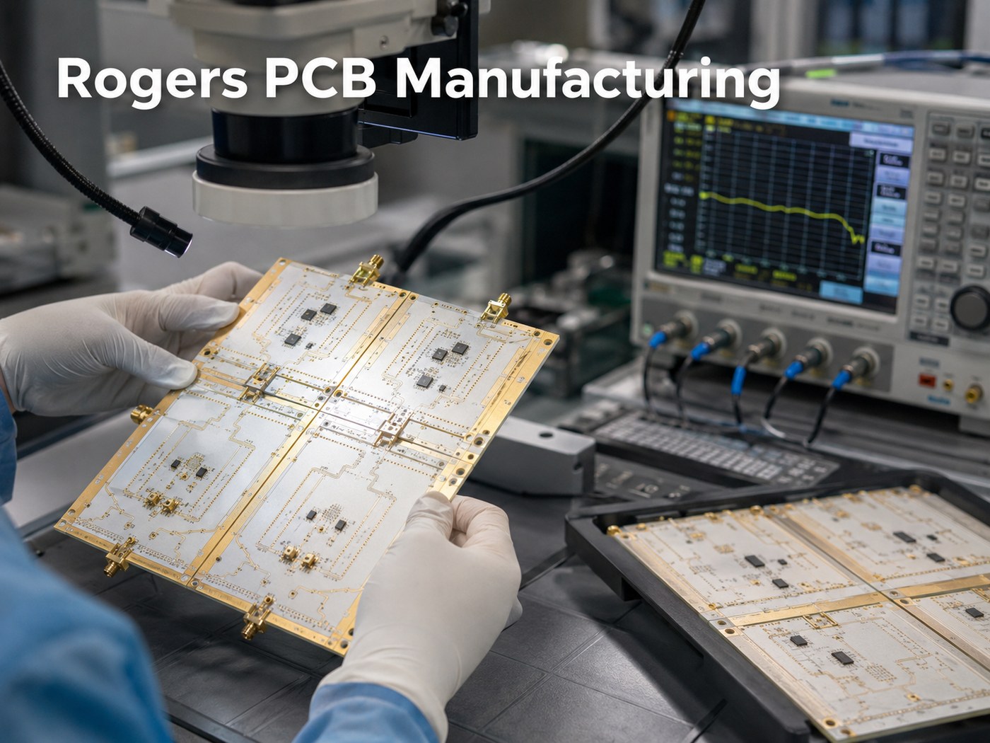
The basic fabrication flow is similar to conventional multilayer PCB production:
- Material preparation
- Inner-layer imaging and etching
- Surface preparation
- Layup and lamination
- Drilling
- Hole-wall preparation
- Copper plating
- Outer-layer imaging and etching
- Solder mask
- Surface finish
- Routing
- Electrical testing
- Impedance verification
- Final inspection
The process details vary according to the Rogers material family.
| Process Area | RO4000 Series | PTFE-Based Rogers Materials |
|---|---|---|
| Material system | Hydrocarbon/ceramic | PTFE-based |
| Processing | Closer to epoxy/glass fabrication | More specialized |
| Hole preparation | Relatively conventional | PTFE-specific preparation may be required |
| Drilling | Similar to rigid laminate processing | Requires tighter process control |
| Multilayer bonding | Conventional high-frequency route | Depends strongly on PTFE system |
RO4003C and RO4350B are generally easier to integrate into conventional multilayer production than PTFE-based materials such as RT/duroid 5880.
What Affects Rogers PCB Price?
Rogers PCB pricing depends on both material cost and fabrication complexity.
| Cost Factor | Effect on Price |
|---|---|
| Rogers laminate grade | Different material families have different costs |
| Dielectric thickness | Affects sourcing and material availability |
| Copper weight | Heavier copper increases material and processing cost |
| Board size | Larger boards use more laminate |
| Panel utilization | Poor nesting wastes expensive material |
| Layer count | More layers require more material and processing |
| Hybrid construction | Can reduce Rogers usage but adds lamination complexity |
| PTFE processing | Requires more specialized fabrication |
| Controlled impedance | Requires stackup and process verification |
| Tolerance | Tighter tolerances increase process control |
| Surface finish | Finish choice affects fabrication cost |
| Quantity | Low-volume builds carry higher setup cost per board |
For accurate quoting, specify the exact Rogers laminate whenever the material cannot be substituted.
How Do You Choose a Rogers PCB Manufacturer?
A capable Rogers PCB manufacturer should understand both the material and the RF design requirements behind it.
Before ordering, check whether the supplier can:
- Confirm the exact Rogers laminate grade
- Source the required dielectric thickness
- Support the specified copper construction
- Process both RO4000 and PTFE materials
- Build Rogers/FR4 hybrid stackups
- Review controlled-impedance structures
- Provide impedance coupons when required
- Control RF trace etching
- Maintain material traceability
- Support prototypes and production quantities
Your RFQ should normally include:
- Gerber files
- Drill files
- PCB drawing
- Stackup
- Rogers material grade
- Dielectric thickness
- Copper weight
- Finished PCB thickness
- Surface finish
- Impedance requirements
- Quantity
- Special inspection requirements
Why Choose EBest Circuit as Your Rogers PCB Manufacturer?
Rogers PCB production requires more than purchasing the correct laminate. Stackup design, impedance geometry, drilling, lamination, etching, and testing all need to be coordinated before production.
EBest Circuit supports:
- Rogers PCB fabrication
- Rogers/FR4 hybrid PCBs
- Controlled-impedance boards
- Multilayer high-frequency PCBs
- DFM and stackup review
- PCB prototyping
- Volume production
- PCB assembly
For Rogers PCB projects, engineering review can cover the laminate grade, dielectric thickness, copper requirement, stackup, and impedance targets before fabrication.
EBest Circuit also operates under quality systems supporting multiple industries, including:
| Certification / Compliance | Application |
|---|---|
| ISO 9001 | General quality management |
| ISO 13485 | Medical electronics |
| IATF 16949 | Automotive electronics |
| AS9100D | Aerospace electronics |
| UL | PCB safety recognition |
| RoHS / REACH | Environmental compliance |
Customers can send Gerber files and specifications for DFM and stackup review before production, which is especially useful for hybrid Rogers/FR4 boards and controlled-impedance RF designs.
Where Are Rogers PCBs Used?
Rogers materials are commonly used where dielectric loss, impedance, or phase directly affects circuit performance.
| Application | Why Rogers Material Is Used |
|---|---|
| RF and microwave circuits | Low transmission loss and controlled impedance |
| Patch antennas | Stable Dk and dielectric thickness |
| Phased-array antennas | Phase consistency and lower feed-network loss |
| Automotive radar | Stable performance at mmWave frequencies |
| 5G infrastructure | Low-loss RF transmission |
| Satellite communication | Microwave loss and phase stability |
| Aerospace RF systems | Stable high-frequency performance |
| RF power amplifiers | Controlled transmission structures |
| Filters and couplers | Accurate impedance and electrical length |
| High-speed communication | Reduced transmission loss in demanding channels |
Material selection should still be based on the actual operating frequency, insertion-loss budget, impedance target, and stackup rather than the application name alone.
FAQs About Rogers PCB
Is Rogers PCB Better Than FR4?
Rogers is not automatically better for every circuit. It is usually selected when lower dielectric loss, tighter Dk control, or more predictable RF behavior is required. FR4 remains more economical for general digital, control, power, and less demanding high-frequency designs.
Is Rogers PCB the Same as a PTFE PCB?
No. Some Rogers materials are PTFE-based, while others are not. RO3003 and RT/duroid 5880 are PTFE-based materials. RO4003C and RO4350B belong to Rogers’ hydrocarbon/ceramic RO4000 family.
What Is the Dielectric Constant of Rogers PCB?
There is no single Rogers PCB dielectric constant. It depends on the laminate. Typical Process Dk values include 3.38 for RO4003C, 3.48 for RO4350B, 3.00 for RO3003, and 2.20 for RT/duroid 5880.
Can Rogers Material Be Used in a Multilayer PCB?
Yes. Rogers laminates can be used in multilayer boards, including hybrid stackups that combine Rogers material with FR4. The bonding system and complete stackup should be reviewed before fabrication.
Why Is Rogers PCB More Expensive Than FR4?
Rogers laminates are specialized high-frequency materials and generally cost more than standard FR4. PTFE processing, controlled impedance, multilayer construction, tight tolerances, low production quantities, and poor panel utilization can further increase the final PCB price.
Need a Rogers PCB for Your High-Frequency Project?
If you need a Rogers PCB for an RF, microwave, antenna, radar, or other high-frequency project, send your Gerber files and basic PCB specifications directly to sales@bestpcbs.com.
For controlled-impedance designs, please also include the stackup, material grade, dielectric thickness, copper weight, target impedance, and operating frequency. Our engineering team will perform a DFM review and send you a quotation within 12 hours.