An SMA terminal PCB is used when an RF signal needs to move between a printed circuit board and an external coaxial cable, antenna, test instrument, or RF module. For engineers and buyers, the question is usually not only “Which SMA connector should I buy?” but “Can this connector be mounted, soldered, grounded, inspected, and assembled reliably on my PCB?”
That is where PCB and PCBA manufacturing review becomes important. The SMA terminal area may involve PCB thickness, connector drawing, footprint accuracy, 50 ohm signal routing, ground pads, edge plating, soldering method, mechanical stress, and final inspection. EBest Circuit (Best Technology) supports RF-related PCB fabrication, component sourcing, SMT assembly, through-hole soldering, inspection, and small-batch PCBA projects where connector reliability matters. If your project includes SMA connectors, RF terminals, antenna interfaces, or connector-sensitive PCBA requirements, please send your Gerber files, BOM, stackup, connector drawing, and assembly notes to sales@bestpcbs.com for engineering review before production.
What Is an SMA Terminal PCB?
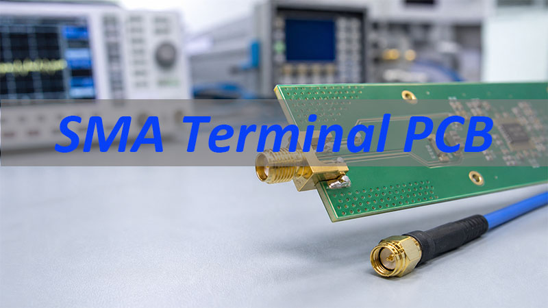
An SMA terminal PCB is a printed circuit board designed with an SMA connector or SMA terminal interface. SMA connectors are widely used for RF signals because they provide a compact coaxial connection between the PCB and external RF equipment.
| Term | Common Meaning |
|---|---|
| SMA terminal PCB | Board with an SMA terminal or connector interface |
| PCB SMA connector | SMA connector mounted on a PCB |
| SMA connector PCB | PCB designed for SMA connector installation |
| RF SMA connector | SMA connector used for RF signal transfer |
| SMA connector receptacle | Female SMA connector interface |
| SMA panel mount connector | SMA connector mounted through a panel or enclosure |
In real projects, the SMA terminal is not only a mechanical connector. It affects the RF transition, grounding path, soldering process, connector strength, cable access, and final inspection.
SMA Terminal PCB vs PCB SMA Connector
An SMA terminal PCB and a PCB SMA connector are closely related, but they do not mean exactly the same thing. The connector is the component. The PCB is the manufactured board that must support the connector correctly.
| Item | SMA Terminal PCB | PCB SMA Connector |
|---|---|---|
| Main focus | Board and connector integration | Connector component |
| Checked by | PCB/PCBA manufacturer | Connector supplier and customer |
| Key details | Footprint, board thickness, RF path, soldering | Gender, frequency, impedance, mounting style |
| Risk | Wrong layout or weak assembly | Wrong connector type or unavailable part |
If the project uses an SMA connector PCB, the connector drawing, PCB footprint, stackup, board thickness, and assembly notes should be checked together. A correct connector part number alone does not guarantee reliable PCBA assembly.
RF SMA Connector Types for PCB Mounting
Different RF SMA connector types require different PCB and assembly checks. The right choice depends on the customer design, enclosure structure, RF path, cable direction, and mechanical requirement.
| SMA Type | Typical Use |
|---|---|
| Edge launch SMA connector | RF signal enters from board edge |
| Surface mount SMA connector | Compact SMT-friendly boards |
| Through-hole SMA connector | Stronger mechanical mounting |
| Right-angle SMA connector | Cable exits parallel to the PCB |
| SMA flange connector | Panel or enclosure mounting |
| SMA female panel mount connector | External cable access through housing |
For PCB manufacturing, the connector type affects pad shape, drill holes, solder mask opening, edge clearance, plating, panelization, and inspection. For PCBA, it affects soldering method, fixture support, cleaning, and packing.
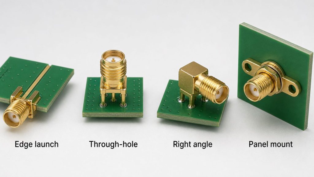
Edge Launch SMA Connector for RF PCB Applications
An edge launch SMA connector is mounted at the edge of the PCB. It is common in RF test boards, antenna boards, wireless modules, high-frequency boards, and measurement interfaces.
Important manufacturing checks include:
- Finished PCB thickness must match the connector drawing.
- The board edge should support the connector body correctly.
- The signal trace should transition cleanly into the connector pin.
- Ground pads and vias should follow the approved RF layout.
- Solder mask opening should not interfere with contact or soldering.
- Panelization should protect the board edge and connector area.
For an edge launch SMA terminal PCB, the board thickness is especially important. Many edge launch connectors are designed for specific PCB thickness ranges. If the finished PCB is too thick or too thin, the connector may not sit correctly, and the RF transition may become unreliable.
For high-frequency projects, the SMA terminal area is often reviewed together with RF PCB manufacturer requirements such as material, copper thickness, impedance, surface finish, and ground continuity.
SMA Flange Connector and Panel Mount Options
An SMA flange connector or SMA panel mount connector is useful when the connector must be fixed to an enclosure, bracket, panel, or mechanical structure. This can reduce stress on the PCB when the cable is connected or disconnected repeatedly.
These projects should check:
- mounting hole diameter and tolerance
- connector body clearance
- panel thickness and connector thread length
- board-to-panel alignment
- soldering or cable connection method
- mechanical stress on the solder joint
- packing protection for protruding connectors
If the SMA connector is fixed to the panel but also connected to the PCB, the mechanical stack should be confirmed before assembly. A small mismatch between PCB, enclosure, and connector can create stress during final product assembly.
SMA Connector Receptacle and Terminal Structure
An SMA connector receptacle is usually the female SMA interface. For PCB and PCBA review, the important point is how the connector terminals contact the board.
Center pin: The center pin carries the RF signal. Its pad, trace width, transition shape, and soldering condition affect signal performance.
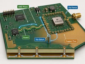
Ground terminals: The outer conductor and ground terminals provide the return path and shielding reference. Ground pad design, via placement, copper connection, and soldering quality should follow the approved RF layout.
Mounting structure: Some SMA connectors rely on SMT pads, some use through-hole legs, and some require screws or flange mounting. The PCB drawing and assembly notes should make this clear before production.
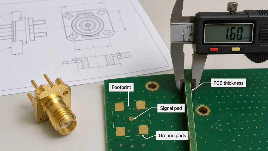
SMA Connector Drawing, Footprint, and PCB Thickness Checks
The SMA connector drawing is one of the most important documents for an SMA terminal PCB project. A small footprint mismatch can cause soldering defects, poor connector seating, weak mechanical support, or unusable RF performance.
Before PCB fabrication and assembly, EBest Circuit checks whether the customer files clearly define:
- exact connector part number
- manufacturer drawing
- PCB land pattern
- drill size and hole plating
- board thickness requirement
- edge clearance
- solder mask opening
- surface finish
- connector orientation
- SMT or through-hole process notes
The SMA connector PCB footprint should be checked against the datasheet, not copied from a similar connector without confirmation. Similar-looking SMA connectors may have different pin dimensions, mounting holes, body height, or recommended board thickness.
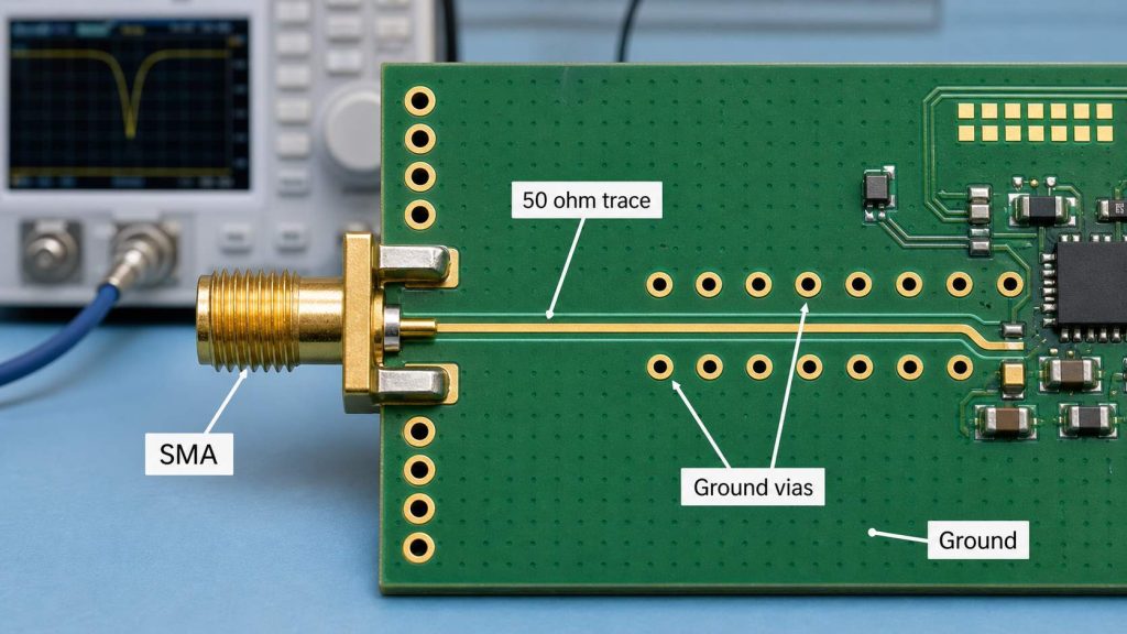
50 Ohm SMA PCB Layout and Grounding Review
Many SMA terminal PCB projects involve 50 ohm RF signal routing. The customer usually defines the circuit and RF design requirements. The PCB manufacturer should not change the RF structure without approval, but it should check whether the files are manufacturable.
Manufacturing review often focuses on:
- stackup and dielectric thickness
- copper thickness
- trace width and spacing
- reference ground layer
- ground via placement near the SMA area
- solder mask opening around RF pads
- surface finish selection
- impedance coupon and test report requirements
For RF boards, the SMA terminal should be reviewed together with the whole signal path. If the board also includes an antenna section, RF module, or coaxial interface, the RF transition should stay consistent with the approved customer design. This is also why RF antenna PCB projects often need early stackup and impedance review.
SMA Connector Soldering and PCBA Assembly Risks
SMA connectors can create assembly risk because they are both electrical parts and mechanical interfaces. A connector may pass visual inspection at first but fail later if soldering, alignment, or mechanical support is weak.
| Assembly Point | Why It Matters |
|---|---|
| Connector orientation | Prevents wrong cable direction |
| Soldering method | SMT and through-hole require different control |
| Stencil opening | Affects solder volume for SMT connectors |
| Manual solder notes | Reduces inconsistent workmanship |
| Visual inspection | Checks connector position and solder fillet |
| Cleaning requirement | Controls flux residue near RF area |
| Packing method | Protects protruding connectors |
For prototype and small volume PCB assembly, the connector area deserves special attention because debugging often depends on stable cable connection, clean signal transfer, and repeatable test setup.
SMA Terminal PCB Manufacturing Case Study
A USA customer needed a prototype RF interface board for a wireless test module. The board used SMA terminal connections for RF signal input and output, so the customer cared about connector seating, board thickness, soldering strength, 50 ohm signal transition, and test reliability.
Project requirements
- Customer region: USA
- Application: wireless RF test module
- Quantity: 20 pcs prototype and pilot build
- PCB type: 4-layer FR4 PCB
- Material: FR4 Tg130
- Copper: 1oz outer copper, 0.5oz inner copper
- Finished thickness: 1.60mm +/-10%
- Surface finish: ENIG 1u”
- Solder mask and silkscreen: green solder mask, white silkscreen
- Assembly: component sourcing by EBest Circuit, SMT and connector assembly
- Delivery: single-unit packing after assembly
- Production control: production files confirmed before fabrication
Customer concerns
- The SMA connector had to sit correctly on the board edge.
- The RF path needed stable 50 ohm transition from connector to PCB trace.
- The connector area could not be damaged during depaneling or packing.
- The prototype quantity was small, but the test setup depended on repeatable connector quality.
EBest Circuit solution
- Reviewed the connector drawing, footprint, and finished PCB thickness before fabrication.
- Checked stackup, copper thickness, and RF trace area for manufacturability.
- Confirmed solder mask opening and connector orientation before SMT.
- Arranged component sourcing and assembly under one workflow.
- Used ENIG for stable solderability and surface protection.
- Checked connector soldering and board cleanliness before single-unit packing.
Result: The customer received a small-batch RF prototype that matched the SMA terminal mounting requirement, PCB thickness target, surface finish, and assembly notes. The value of the project was not only producing 20 boards. It was reducing the risk that an RF test module would fail because of a connector footprint, board-edge, soldering, or packing issue.
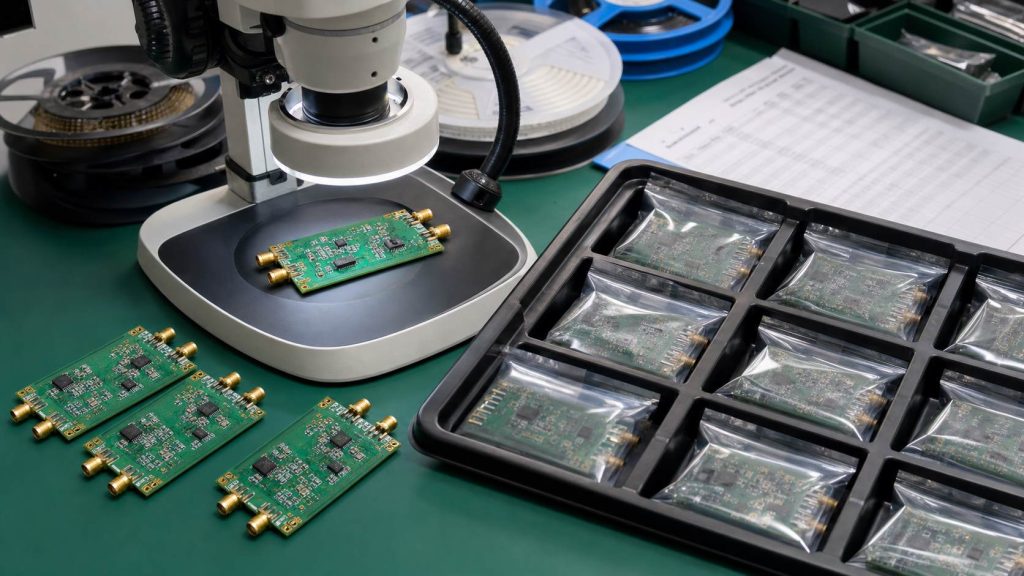
Why Choose EBest Circuit for SMA Terminal PCB and PCBA Projects?
EBest Circuit is suitable for SMA terminal PCB and PCBA projects when connector reliability, RF signal routing, and manufacturing review must be controlled together.
Useful support includes:
- RF-related PCB fabrication
- FR4, high-frequency, metal core, ceramic, flex, and rigid-flex PCB support
- stackup and impedance review when required
- connector drawing and footprint review
- BOM sourcing and approved component preparation
- SMT, through-hole, and mixed assembly
- inspection, testing coordination, and packing support
- prototype, pilot run, and small-batch production
EBest Circuit has worked in PCB and PCBA manufacturing since 2006. The company supports customers in more than 40 countries and regions, with major export markets including the USA, Germany, and Israel. Quality support includes ISO9001, ISO13485, IATF16949, AS9100D, RoHS, REACH, and UL-related documentation.
For connector-sensitive projects, stable communication also matters. Many engineers, quality managers, production leaders, and sales members at EBest Circuit have worked in the company for more than 10 years. That experience helps keep connector drawings, stackup notes, BOM changes, assembly requirements, and packing details visible from file review to delivery.
FAQs About SMA Terminal PCB
1. What is an SMA terminal PCB?
An SMA terminal PCB is a printed circuit board designed with an SMA connector or terminal interface for RF signal connection to coaxial cable, antenna, RF module, or test equipment.
2. Is an SMA terminal PCB the same as an SMA connector PCB?
They are closely related. An SMA connector PCB usually refers to a PCB designed for SMA connector installation. An SMA terminal PCB emphasizes the connector interface area and how it is manufactured and assembled.
3. What PCB thickness is used for SMA edge launch connectors?
It depends on the connector drawing. Many edge launch SMA connectors are designed for specific board thicknesses, so the datasheet and finished PCB thickness tolerance should be confirmed before production.
4. Does an SMA terminal PCB need 50 ohm impedance control?
Many RF SMA connector projects require 50 ohm routing, but the exact requirement should come from the customer’s RF design. The PCB manufacturer can help review stackup, trace geometry, copper thickness, and impedance report requirements.
5. Can EBest Circuit help choose the SMA connector?
EBest Circuit can help review connector availability, footprint, assembly method, and manufacturability. The final connector model and RF performance decision should be confirmed by the customer’s engineering team.
All in all, an SMA terminal PCB project is not only about placing a connector on a board. It is about making sure the connector drawing, footprint, PCB thickness, RF path, grounding, soldering, inspection, and packing method work together before production starts. If your project includes SMA connectors, RF terminals, antenna interfaces, or connector-sensitive PCBA requirements, please send your Gerber files, BOM, stackup, connector drawing, and assembly notes to sales@bestpcbs.com. EBest Circuit’s engineering team can review the manufacturing path before your boards move into production.