PCB manufacturing PCB manufacturing
Home > Blog

TDA7294 Amplifier Board: A Comprehensive Introduction

August 13th, 2024

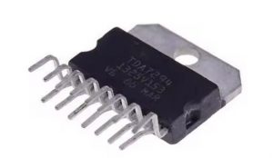
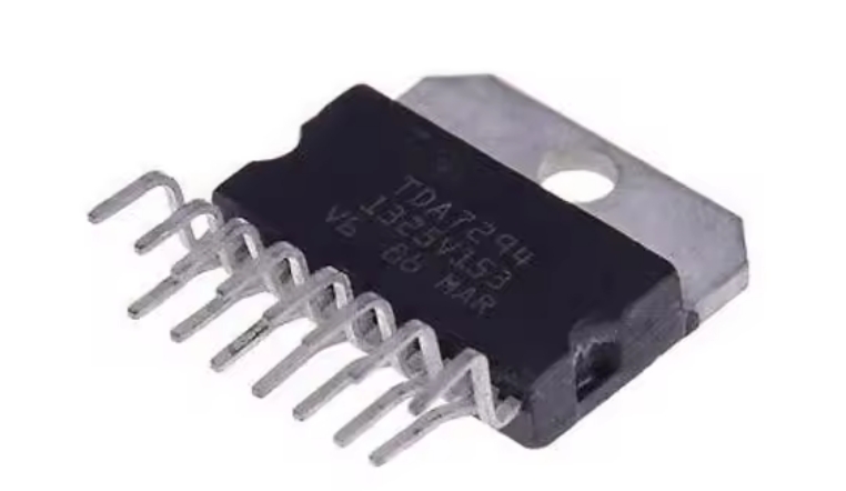
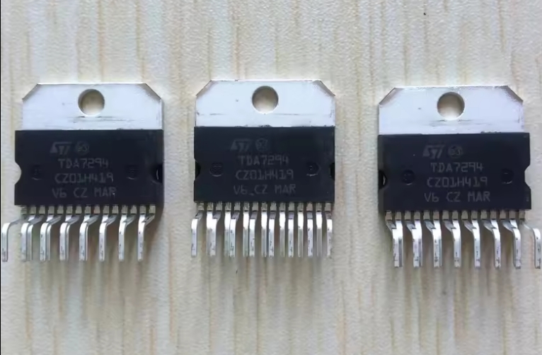
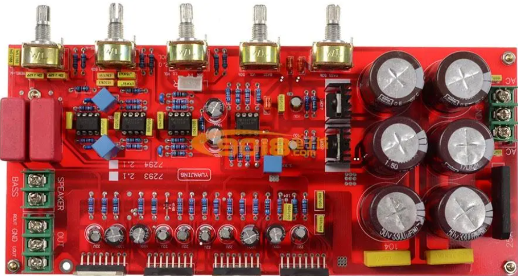
The TDA7294 amplifier board is a functional and widely used audio amplifier. It is based on the TDA7294 integrated circuit (IC), a high-power, low-distortion audio amplifier IC developed by STMicroelectronics. This IC is designed to deliver high-quality audio output with minimal distortion, making it a popular choice for DIY audio enthusiasts and professionals alike.

What is TDA7294 IC Amplifier Board?

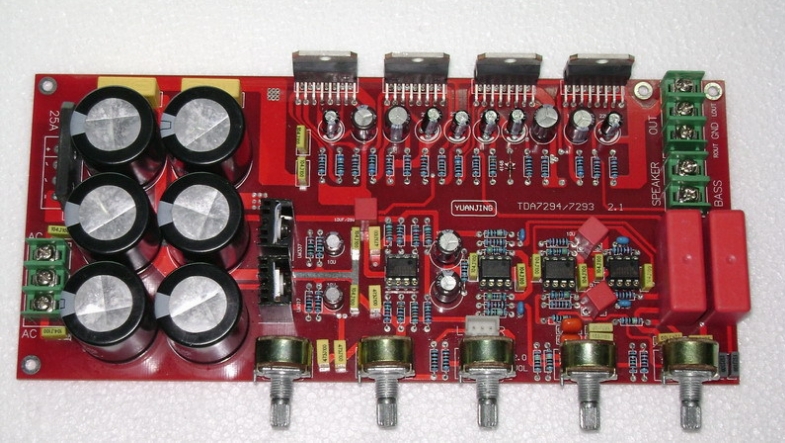
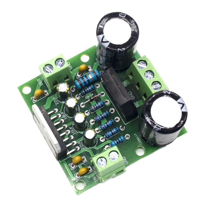
The TDA7294 IC is capable of delivering up to 100 watts of power in a single-ended or bridged configuration, making it suitable for a wide range of audio applications, from home audio systems to professional audio equipment. The amplifier board typically includes the TDA7294 IC along with supporting components such as capacitors, resistors, and heatsinks, all mounted on a printed circuit board (PCB). This board is designed to simplify the process of building a powerful and reliable audio amplifier by providing a pre-configured layout that ensures optimal performance.
TDA7294 Amplifier Board: A Comprehensive Introduction

Features of TDA7294 Amplifier Board

The TDA7294 amplifier board provides several key features that make it a popular choice for high-quality audio amplification.

  • High Output Power
  • Low Distortion
  • Built-in Protection Circuits
  • Thermal Management
  • Low Noise and High Signal-to-Noise Ratio (SNR)
  • Ease of Integration
  • Flexible Configuration
  • Improved Reliability
  • Compact Size

TDA7294 Amplifier Circuit Diagram

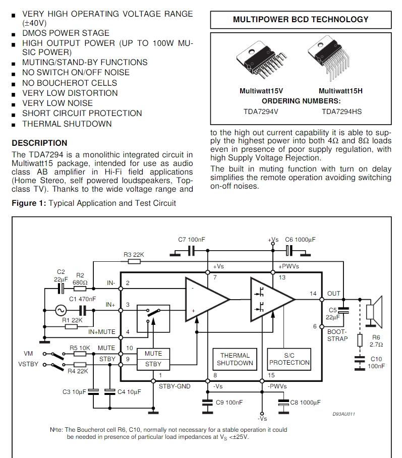
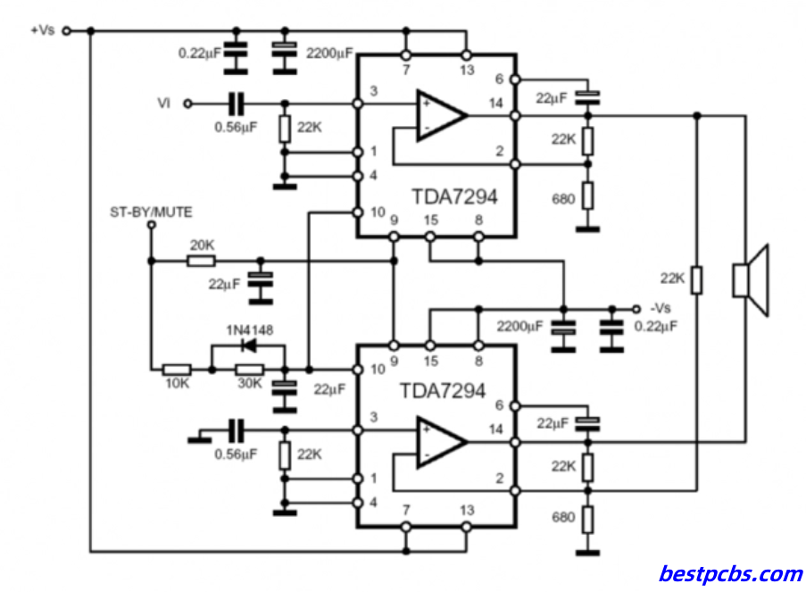
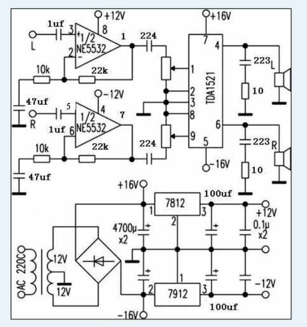
The circuit diagram of the TDA7294 amplifier is a crucial element for anyone looking to build or understand this amplifier. The diagram typically includes the TDA7294 IC at the core, surrounded by components that shape the audio signal and manage power delivery. Key components include capacitors for signal coupling and power supply smoothing, resistors for setting gain and biasing, and inductors or filters for noise reduction.
TDA7294 Amplifier Board: A Comprehensive Introduction

The TDA7294 IC itself has several pins that serve specific functions in the circuit. For instance, the input pin receives the audio signal, while the output pin sends the amplified signal to the speakers. Power supply pins connect to the positive and negative voltage rails, and other pins might be used for muting, standby, or feedback purposes.

When assembling the circuit, careful attention must be paid to the placement of components and routing of traces on the PCB to minimize noise and maximize performance. The layout of the circuit diagram ensures that the amplifier delivers clean, high-fidelity sound with minimal distortion, which is a key selling point for the TDA7294.

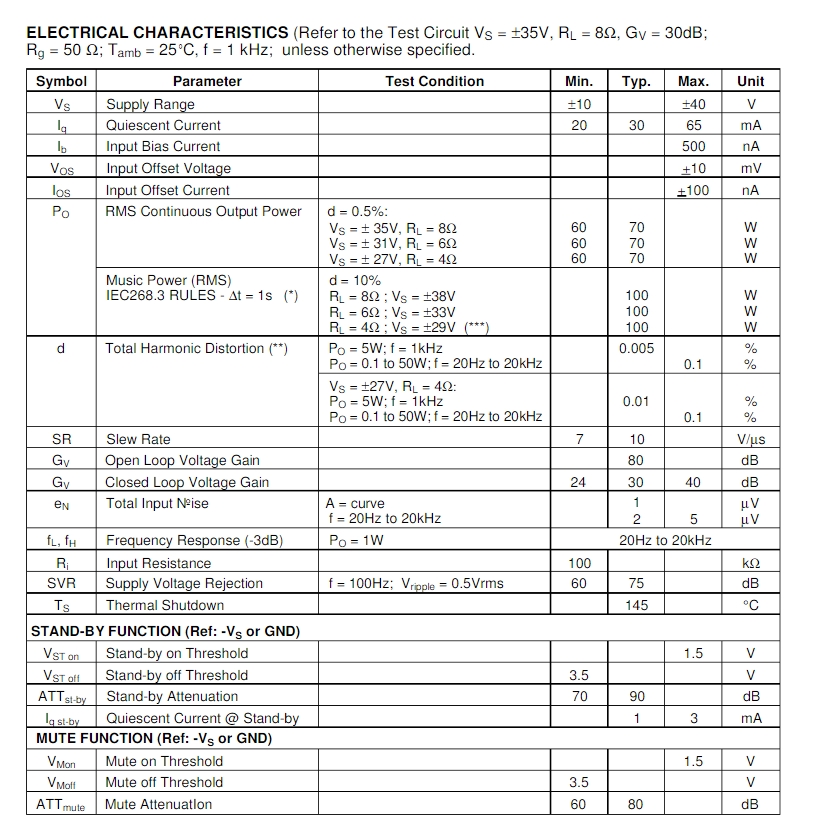
TDA7294 Specification

SymbolParameterTest conditionMin. valueTypical valueMax. valueUnit
VsPower Supply Ā±10 Ā±40V
lqCurrent Consumption 203060mA
VosInput Offset Voltage   500mV
losInput Offset Current   Ā±100nA
PoContinuous Power OutputVS = ± 35V, RL = 8Ī©; VS = ± 31V, RL = 6Ī©; VS = ± 27V, RL = 4Ī©;  6070 W
dTHDPO = 5W; f = 1kHz PO = 0.1 to 50W; f = 20Hz to 20kHz 0.0050.01%
VS = ±27V, RL = 4W: PO = 5W; f = 1kHz PO = 0.1 to 50W; f = 20Hz to 20kHz   0.010.01%
SRSwitching rate 710 V/us
GvOpen Loop Voltage Gain  80 dB
GvClosed Loop Voltage Gain 243040dB
fL, fHFrequency Response (-3dB)Po=1W20Hz to 20kHz
RiInput Resistance 100  KĪ©

TDA7294 Pinout

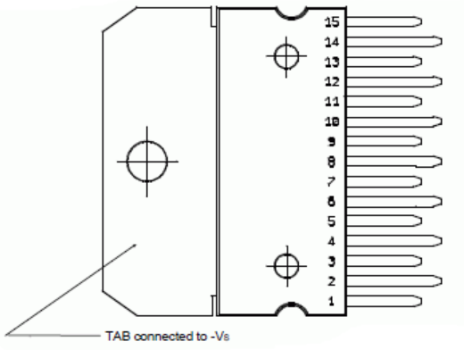
The TDA7294 IC comes with a specific pinout configuration that plays a crucial role in its operation. The chip has 15 pins, each with a designated function:
TDA7294 Amplifier Board: A Comprehensive Introduction

Pin 1 (IN+): Non-inverting input

Pin 2 (SVR): Supply voltage rejection

Pin 3 (IN-): Inverting input

Pin 4 (MUTE): Mute function

Pin 5 (ST-BY): Standby function

Pin 6 (VCC+): Positive supply voltage

Pin 7 (OUT): Output

Pin 8 (GND): Ground

Pin 9 (BOOTSTRAP): Bootstrap capacitor

Pin 10 (NC): Not connected

Pin 11 (VCC-): Negative supply voltage

Pin 12 (DIAG): Diagnostics pin

Pin 13 (BOOTSTRAP): Bootstrap capacitor

Pin 14 (GND): Ground

Pin 15 (OUT): Output

TDA7294 Datasheet

The TDA7294 datasheet is a critical resource for anyone working with this IC. It provides detailed information about the IC’s electrical characteristics, pin configurations, thermal properties, and recommended operating conditions. The datasheet also includes typical application circuits, which can serve as a starting point for designing your own amplifier.

In addition to technical specifications, the datasheet often includes practical advice on PCB layout, component selection, and thermal management. Following these guidelines can help you achieve the best possible performance from your TDA7294 amplifier board.

How Many Watts is a TDA7294 Output?

The TDA7294 IC is capable of delivering up to 100 watts of output power when configured in a single-ended or bridged amplifier circuit. The actual output power depends on several factors, including the supply voltage, load impedance, and heat dissipation. In a typical configuration with a supply voltage of ±35V and an 8-ohm load, the TDA7294 can deliver around 70 watts of continuous power.

For higher power output, the IC can be used in a bridged configuration, where two TDA7294 ICs are combined to drive a single load. In this setup, the output power can reach up to 150 watts, making it suitable for driving larger speakers or subwoofers.

It’s important to note that the power rating of the TDA7294 should be matched to the speakers and other components in your audio system. Overloading the IC by driving it at maximum power for extended periods can lead to overheating and potential damage, so proper thermal management is essential.

What is the Equivalent of TDA7294?

When looking for an equivalent to the TDA7294, there are a few other audio amplifier ICs that offer similar performance characteristics. Some of the commonly considered alternatives include:

  • LM3886

This is another high-power audio amplifier IC that delivers up to 68 watts of output power. It’s known for its low distortion and high fidelity, making it a popular choice for DIY audio projects.

  • TDA7293

This IC is very similar to the TDA7294, with slightly different electrical characteristics. It can be used as a drop-in replacement in many circuits, offering similar power output and performance.

  • TDA2030

While not as powerful as the TDA7294, this IC is a good alternative for lower-power applications. It delivers up to 20 watts of output power and is widely used in small audio amplifier projects.

Each of these alternatives has its strengths and weaknesses, so the best choice depends on the specific requirements of your project. For instance, if you need higher output power, the LM3886 might be a better option, while the TDA2030 is more suitable for compact, low-power designs.

What is the Maximum Voltage for TDA7294 IC?

The maximum supply voltage for the TDA7294 IC is ±50V. However, for optimal performance and reliability, it’s recommended to operate the IC at a lower voltage, typically around ±35V to ±40V. Operating at the maximum voltage can increase the risk of overheating and may require additional cooling measures, such as larger heatsinks or active cooling.

The voltage rating is crucial for ensuring the longevity and performance of the amplifier. Exceeding the maximum voltage can cause the IC to fail, leading to permanent damage. Therefore, it’s important to choose a power supply that matches the recommended voltage range for the TDA7294.

In addition to the supply voltage, the IC’s thermal management is also important. Ensuring adequate cooling through heatsinks or ventilation can prevent overheating and ensure stable operation, especially when driving the amplifier at high power levels.

What is TDA in an Amplifier?

The TDA prefix in TDA7294 refers to the series of audio amplifier ICs developed by STMicroelectronics. These ICs are designed to provide high-quality audio amplification with minimal distortion and noise. The TDA series includes a range of ICs with varying power output capabilities, making them suitable for different audio applications, from small portable speakers to large home audio systems.

In an amplifier, the TDA IC is responsible for amplifying the audio signal from a low-level input to a high-level output that can drive speakers. The IC’s internal circuitry is optimized for audio performance, ensuring that the amplified signal remains clear and distortion-free.

The TDA series is widely regarded for its reliability and performance, making it a popular choice for both commercial and DIY audio projects. Whether you’re building a simple audio amplifier or a more complex audio system, the TDA7294 and its counterparts offer a solid foundation for high-quality sound.

FAQs

1. Can the TDA7294 be used in a car audio system?

Yes, the TDA7294 can be used in car audio systems, but you need to ensure that the power supply provides the correct voltage and current. Car audio systems typically operate at 12V, so a step-up converter might be needed to reach the required supply voltage.

2. How do I connect multiple TDA7294 ICs for higher power output?

You can connect multiple TDA7294 ICs in a bridged configuration to increase the power output. This involves using two ICs to drive a single load, effectively doubling the output power.

3. What is the typical distortion level of the TDA7294?

The TDA7294 has a low distortion level, typically around 0.005% at 1kHz, making it suitable for high-fidelity audio applications.

4. Is the TDA7294 suitable for subwoofers?

Yes, the TDA7294 is suitable for driving subwoofers, especially in a bridged configuration where it can deliver high power output with low distortion.

5. Can I use the TDA7294 with a passive cooling system?

While the TDA7294 can be used with a passive cooling system, it’s important to ensure that the heatsink is large enough to dissipate the heat generated during operation. For higher power levels, active cooling may be necessary to prevent overheating.
You may also like

Rigid flex pcb Design & Prototype Right the First Time

August 12th, 2024

rigid-flex printed circuit board ,Rigid flex pcb manufacturer. More than 5 years design team of 10 people. Quick proofing within 1 week. A 3,000-square-meter factory for small batch to mass production and assembly.

What is a rigid flex pcb?

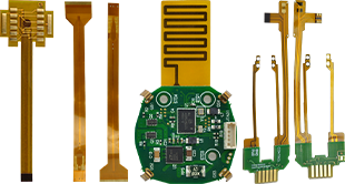
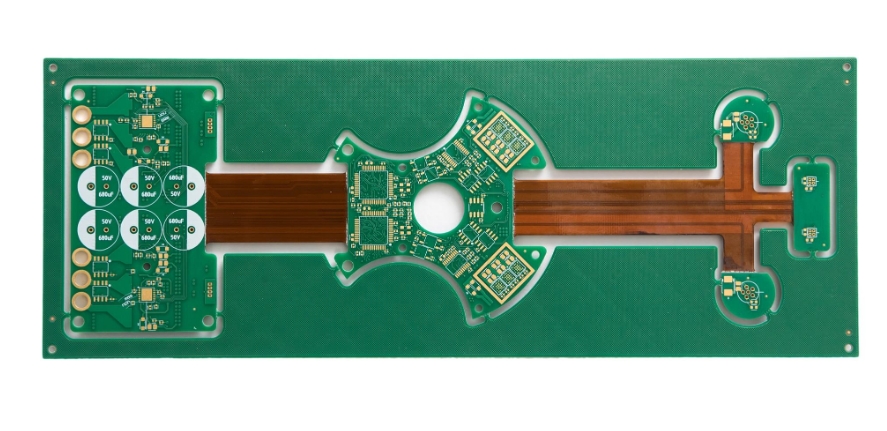
Rigid flex pcb,rigid-flex printed circuit board,Rigid flex circuit are a hybrid construction flex circuit consisting of rigid and flexible substrates which are laminated together into a single structure. Each layer of rigid-flex circuit are electrically interconnected by plated through holes (PTH), which is different from a flexible circuit with FR4/PI stiffener on top or bottom of flex circuit only by the means of presensive or thermal senstive adhesive only, no PTH.

What is a rigid flex pcb?

Rigid-flex PCBs can be divided into single-sided boards, double-sided boards and multi-layer boards according to the number of conductive circuit layers. Multi-layer boards usually contain multiple rigid layers and flexible layers, and the circuits are connected and interconnected through interlayer connections.

Is Rigid flex PCB reliable?

  1. Design and manufacturing efficiency: Designers of rigid-flex boards can use a single component to replace a composite printed circuit board connected by multiple connectors, multiple cables and ribbon cables, which not only has stronger performance and higher stability, but also limits the scope of the design to one component, optimizing the available space by bending and folding the lines like a stacked paper swan.
  2. Space and weight optimization: In PCB prototyping for consumer electronics, the use of rigid-flex boards not only maximizes space use and minimizes weight, but also greatly improves reliability, eliminating many needs for solder joints and fragile and fragile wiring that are prone to connection problems. The design of this circuit board allows the size and weight of equipment and systems to be reduced while maintaining functionality.
  3. High stress environment adaptability: Rigid-flex boards also have high impact resistance and can survive in high stress environments, which makes it widely used in military, aviation and medical equipment.
  4. Excellent electrical performance: Rigid-flex boards provide excellent electrical performance, and good thermal conductivity makes components easy to cool. The lower dielectric constant of the flexible part allows for fast transmission of electrical signals, and the PI substrate has a higher glass transition temperature or melting point, which allows the components to operate well at higher temperatures.
  5. Assembly reliability: Rigid-flex boards reduce the hardware required for traditional rigid boards and flexible boards to be connected, such as traditional jumper sockets, etc., and can provide higher assembly reliability.

What is the difference between rigid flex and semi flex?

  1. Definition and structure
    Rigid-flexible board: It is a combination of soft board and hard board, that is, a thin layer of flexible bottom layer and rigid bottom layer are combined and laminated into a single component to form a circuit board1. It changes the traditional flat design concept and expands it to a three-dimensional space concept. It has both rigid layer and flexible layer and is a multi-layer printed circuit board.
    Semi-flexible board: It is a PCB used in the field of static bending obtained by combining controlled deep milling or rigid-flexible board processing technology (such as milling cover or opening window, etc.) in the standard hard board processing process2. It often uses FR4 material, first processes the PCB according to the normal process, and then mills the middle part that needs to be bent to make it flexible.
  2. Flexibility and application
    Rigid-flexible board: It has higher flexibility and can be bent, folded or rounded, and then integrated into various products, such as aerospace equipment, military aircraft, high-end medical equipment, digital cameras, portable cameras and high-quality MP3 players. ā€Œ
    Semi-flexible board: Although it can be bent or curved, its flexibility is not as good as that of rigid-flexible board. It is mainly used in situations where static bending is required, such as endoscopes in medical equipment, injection needle tip protection circuit boards, and medical equipment temperature control circuit boards. ā€Œ
  3. Processing and cost
    Rigid-flexible board: Due to the mixed use of multiple materials and multiple production steps, its processing time is longer and the production cost is higher. ā€Œ
    Semi-flexible board: Although its processing process is also more complicated, its processing cost is lower than that of rigid-flexible board, and it is more suitable in some applications. ā€Œ
  4. Features and advantages
    Rigid-flexible board: It has stronger performance and higher stability, can reduce space and weight, and improve the reliability of connection. ā€Œ
  5. Semi-flexible board: It has the advantages of low cost, good dimensional stability, bendable three-dimensional installation to reduce space, and reduce the number of interfaces during assembly to improve reliability.ā€Œ

how do they add rigid layers to flex pcb?

  1. Design layout: Before starting the manufacturing process, the PCB design layout is first carried out to determine the location and connection method of the components. ā€Œ
  2. Substrate preparation: Clean the laminate containing the copper layer to prepare for the subsequent manufacturing process. ā€Œ
  3. Pattern generation: The generation of circuit patterns is completed by screen printing or photo imaging. ā€Œ
  4. Etching process: The laminate with the circuit pattern is soaked in an etching tank or sprayed with an etchant solution for etching. ā€Œ
  5. Mechanical drilling: Circuit holes, pads and via patterns are drilled using a precision drilling system or technology, such as laser drilling technology. ā€Œ
  6. Copper plating process: Deposit the required copper in the plated vias to establish electrical interconnections between layers. ā€Œ
  7. Covering layer application and lamination: Apply the covering layer material (such as polyimide film) and adhesive, and laminate under specific temperature, pressure and vacuum limits to ensure proper adhesion of the covering layer. ā€Œ
  8. Apply stiffeners: Apply local additional stiffeners before additional lamination processes as required by the board design. ā€Œ
  9. Flexible board cutting: Cut flexible boards from production panels using hydraulic punching methods or specialized punching knives. ā€Œ
  10. Electrical testing and verification: Conduct electrical testing in accordance with IPC-ET-652 guidelines to confirm that the insulation, connection, quality, and performance of the circuit board meet the requirements of the design specifications.

What are the disadvantages of rigid flex PCB?

  1. Material damage or breakage: The flexible materials used in rigid-flex boards are susceptible to flexure and bending. Long-term use or improper handling may cause damage or breakage of the flexible part, resulting in an open circuit.
  2. Poor welding: The manufacture of rigid-flex boards requires welding processes. If the welding is poor or the solder joints are of poor quality, it may cause loose connections or solder joints to fall off, resulting in an open circuit.
  3. Excessive bending or stretching: Excessive bending or stretching during use may cause the connection wires or wires of the flexible part to be stretched excessively and break, causing an open circuit.
  4. Design defects: If the design of the rigid-flex board is unreasonable or defective, such as insufficient design of the overbending area or too small bending radius, the material of the flexible part may be damaged by excessive stress, resulting in an open circuit.
  5. Environmental factors: Under different environmental conditions, it may be affected by factors such as temperature, humidity, and chemicals. Long-term use in harsh environments may cause material aging or corrosion, resulting in an open circuit. ā€Œ
  6. Damage during assembly: During the assembly process, improper operation or external force may cause damage to the connecting wires or wires of the flexible part, resulting in an open circuit.

Application fields of rigid flex PCB

  1. Automotive electronics: Rigid-flex boards are widely used in automotive electronic systems such as dashboards, navigation systems, and in-car entertainment systems in the automotive industry. Their flexibility and high reliability enable them to adapt to the complex spatial layout and vibration environment inside the car.
  2. Medical equipment: In the field of medical equipment, rigid-flex boards also have important applications, such as medical monitoring equipment, medical imaging equipment, etc. Its flexible part can adapt to different equipment shapes and size requirements, while having stable circuit connection performance.
  3. Aerospace field: Rigid-flex boards are usually used in aircraft dashboards, navigation systems, communication equipment, etc. in the aerospace field. Due to their light, thin and flexible characteristics, rigid-flex boards have become an ideal choice for aerospace equipment.
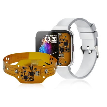
  4. Smart wearable devices: With the rapid development of smart wearable devices, rigid-flex boards are widely used in products such as smart watches and health monitoring equipment. They can be combined with curved display screens, sensors and other components to achieve a more humanized design.
  5. Industrial control field: In the field of industrial automation control, rigid-flex boards are often used in PLC controllers, robot control systems, sensor interfaces, etc. Its flexibility and reliability ensure the stable operation of the equipment in harsh environments.
Application fields of rigid flex PCB

Rigid flex pcb manufacturer

rigid flex pcb.rigid-flex printed circuit board,Rigid flex circuit are a hybrid construction flex circuit consisting of rigid and flexible substrates which are laminated together into a single structure. Each layer of rigid-flex circuit are electrically interconnected by plated through holes (PTH), which is different from a flexible circuit with FR4/PI stiffener on top or bottom of flex circuit only by the means of presensive or thermal senstive adhesive only, no PTH.

Rigid flex pcb manufacturer

Multilayer circuitry-from 3 to 14+ layers
Min LW/LS: 4mil/4mil
Adhesive-based and adhesiveless constructions, including thermoplastic and thermoset stiffener attachment.
Polyimide substrates: 1/2mil – 4mil
Copper: 1/3OZ – 2OZ, RA or ED type
Stiffeners include Polyimide (0.075-0.20mm), FR4 (0.15-2.0mm), and punched or formed metal parts (0.075-1.0mm)
Low-cost, conventional fabrication and lamination completed with PTH based plating
Screened inks, photo-imageable soldermasks, or laminated coverlay dielectrics
Surface finishes: ENIG, electroplated nickel/gold, immersion silver, tin,
EMI Shielding

how to design flex rigid pcb?

Rigid-Flex Circuit Design Guidelines

To form a rigid-flex, follow these considerations to ensure the best results.

Considerations When Designing Rigid-Flex Circuits

To produce a rigid-flex PCB with unmatched quality and functionality, you must follow the correct manufacturing specifications. This is the set guidelines and standards that manufacturers must consider when designing and manufacturing flexible circuit boards.

Determine Manufacturing Process and Materials Beforehand

Depending on the flexibility you require, you need to decide beforehand what materials to use and the methods to use. Example; When the board you are designing only needs to be folded during manufacturing and thereafter be in a fixed position without bending, you can decide the following

  1. Copper type and grade
  2. Manufacturing method
  3. Number of layers to be used.

On the other hand, if the board is for an application with frequent movement, vibration, and impact, you must be clear in choosing the following:

  1. Copper Coils
  2. Adhesives and
  3. Number of Layers

Place Copper Traces at Right Angles to Rigid-Flex

Copperworks is a great fit when placed on the right edge of the board. Avoid bending copper traces at corners as it will pull stress and may not create the best bend. For PCB flex that requires bending, use sharp radius bends to avoid smudging copper traces.

Provide adequate pad support for exposed copper

Repetitive stress from frequent bending can cause copper on the circuit to break away from the polyimide substrate. Support exposed copper with pads to prevent separation.

Use hatched polygons

Hatched polygons instead of solidified copper help maintain the flexibility of flexible PCBs.

Leave at least 1/2mm gap between copper ring and adjacent vias

1/2mm helps avoid fatigue caused by frequent bending. Placing vias in fixed areas of the board helps avoid frequent movement and bending, resulting in the best rigid-flex.

You may also like

What Does An Audio Board Do? – EBest Circuit (Best Technology)

August 9th, 2024

An audio board, often referred to as a soundboard or mixer, is a crucial device in the world of sound engineering. Whether you’re working on a live concert, recording in a studio, or simply enhancing audio for a video production, understanding the role of an audio board is essential. This guide will walk you through what an audio board does, its various names, and how to set one up effectively.

What Does An Audio Board Do? - EBest Circuit (Best Technology)

What Does an Audio Board Do?

An audio board, or soundboard, manages and controls audio signals. It’s used in many settings, from live concerts to recording studios. The primary function of an audio board is to mix different audio sources, such as microphones and instruments, to create a balanced sound output. This device allows sound engineers to adjust levels, equalize sound frequencies, and add effects to enhance the overall audio experience.

In more technical terms, an audio board receives input signals, processes them, and sends them to an output device. This processing can include adjusting volume levels, panning audio between speakers, and applying effects like reverb or delay. The result is a well-mixed audio output that sounds harmonious and professional.

What is Also Called an Audio Board?

An audio board goes by several names, depending on its use and context. Commonly, it’s known as a soundboard or mixing console. In professional settings, you might hear it referred to as an audio mixer or sound mixer. These terms are often used interchangeably, but they all refer to the same essential device that manages and manipulates audio signals.

What Does An Audio Board Do? - EBest Circuit (Best Technology)

Other names include audio mixing board and professional mixing board. These names highlight the device’s role in combining multiple audio inputs into a single or multiple outputs. Whether you’re shopping for an audio board online or looking to upgrade your studio equipment, understanding these terms will help you find the right product for your needs.

What is the Working Principle of Audio Board?

The working principle of audio circuit refers to the process of audio signal transmission and processing in the circuit. In general, the frequency range of audio signals is 20Hz to 20kHz, and they are electrical signals used to transmit sound. The processing of audio signal includes amplification, mixing, filtering and so on.

Amplification refers to increasing the amplitude of the audio signal so that it can drive the speaker to produce a sound. The amplification process is generally achieved using an amplifier, the principle is to use the amplifier tube of the amplifier to amplify the input signal and then output it to the speaker.

Mixing refers to the process of mixing multiple audio signals into one signal. In a mixing circuit, multiple audio signals are mixed together through a mixer to output a composite signal. The mixer is generally composed of an operational amplifier and a mixer. The operational amplifier is responsible for adding multiple input signals, while the mixer is responsible for adjusting the volume ratio of each input signal.

Filtering refers to filtering the audio signal through a filter to remove unwanted frequency components. Filters are generally divided into low-pass filters, high-pass filters and band-pass filters. A low-pass filter only allows low-frequency signals to pass through, a high-pass filter only allows high-frequency signals to pass through, and a bandpass filter only allows signals in a certain frequency range to pass through.

Is a Sound Board the Same as a Mixer?

Yes, a soundboard and a mixer are essentially the same device. Both terms describe equipment used to blend and adjust audio signals. The term “mixer” is often used in professional audio production environments, while “soundboard” is more common in live sound settings.

The confusion between these terms arises from their varied applications. A soundboard is typically associated with live events, where audio engineers manage the sound in real-time. A mixer, on the other hand, might be used more broadly, encompassing both live and studio environments. Regardless of the term, the device’s primary function remains the same: to mix audio signals and produce a balanced sound output.

What is the Function of a Soundboard?

A soundboard, or audio mixer, plays a critical role in sound engineering by managing and manipulating audio signals. Let’s delve deeper into its functions:

  • Mixing Audio Signals
  • Equalization (EQ)
  • Volume Control
  • Panning
  • Adding Effects
  • Routing
  • Dynamic Processing
  • Monitoring

How Do You Hook Up a Soundboard?

Hooking up a soundboard needs to proceed several steps. Each step is the key point to make sure all audio sources are correctly connected and configured. Here’s a step-by-step guide:

  1. Prepare all necessary cables, microphones, instruments, and speakers.
  2. Plug your microphones and instruments into the input channels on the soundboard. Each channel corresponds to a specific input source.
  3. Connect the output channels of the soundboard to your speakers or recording devices. This usually involves using XLR or quarter-inch cables.
  4. Turn on the soundboard and all connected equipment.
  5. Adjust the input gain for each channel to ensure the signal is neither too weak nor too strong.
  6. Test each input and output to ensure everything is working correctly. Make necessary adjustments to the levels and EQ settings.
  7. Use headphones or monitor speakers to listen to the audio and make final adjustments.

How to Set Up a Sound Mixing Board?

Setting up a sound mixing board involves more than just connecting cables. Here are detailed steps to set up your sound mixing board effectively:

  • Plan Your Setup

Determine the layout of your equipment and where each input and output will be connected. This planning stage helps avoid confusion during the actual setup.

  • Label Everything

Label each input and output cable to know which source they correspond to. This step is crucial in complex setups with many audio sources.

  • Connect Your Inputs

Plug in microphones, instruments, and any other audio sources into the appropriate input channels on the mixing board.

  • Connect Your Outputs

Connect the main outputs to your speakers or PA system. Also, connect any auxiliary outputs to additional monitors or recording devices.

  • Power Everything On

Turn on your mixing board and connected equipment. Make sure to power on any external preamps or processors first if you’re using them.

  • Adjust Gain Levels

Set the gain for each input channel. Start with the faders at unity (0 dB) and adjust the gain until each input is at a proper level.

  • Set EQ and Effects

Adjust the EQ settings for each channel to achieve a balanced sound. Add effects as needed to enhance the audio.

  • Create a Mix

Use the faders to balance the levels of all input sources. Make sure each source is heard clearly without overpowering the others.

  • Monitor and Adjust

Continuously monitor the sound through headphones or monitor speakers. Make adjustments as necessary to maintain a balanced mix.

EBest Circuit (Best Technology) has rich experience in the audio board manufacturing, we have served more than 2000+ customers and provide excellent turn-key solutions. If you are interested in the audio board pcb assembly, welcome to contact us.

You may also like

Ā hs code printed circuit board,pcb boards hs code

August 9th, 2024

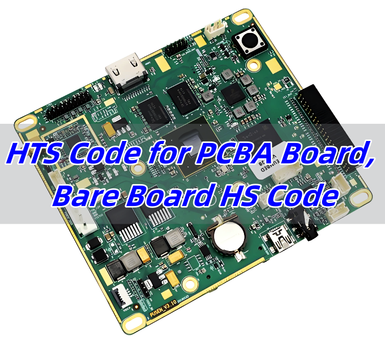
The customs code for printed circuit boards is 8534-0000. 8534 is the classification code for this item, and 0000 represents the sub-classification code under this item. In the actual customs declaration process, it is necessary to select the corresponding sub-classification code according to the specific classification standard of printed circuit boards.

hs code printed circuit board

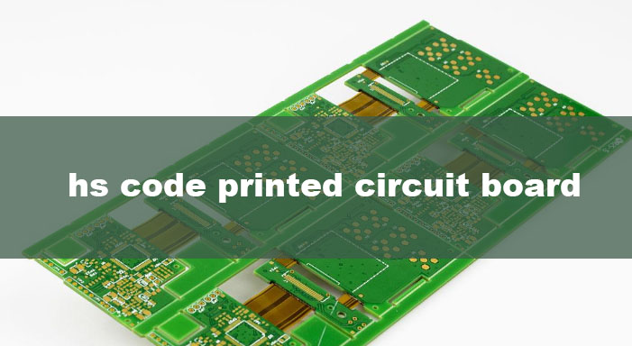
hs code printed circuit board:85340000
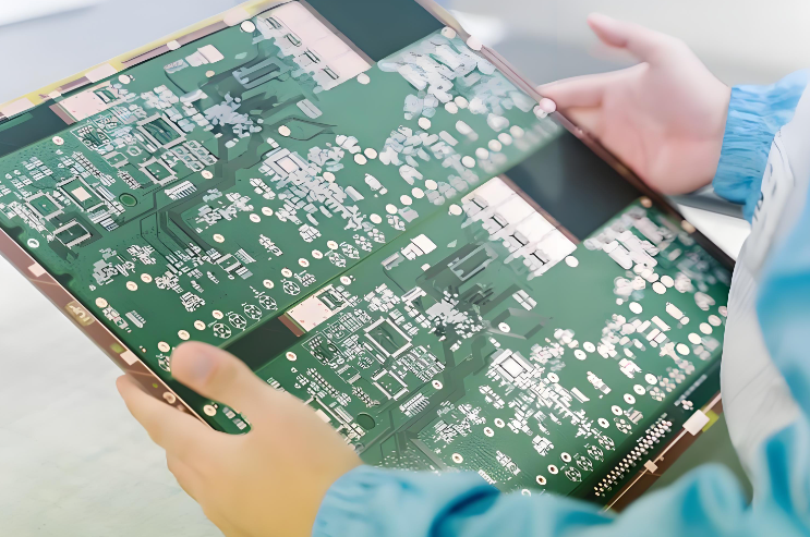
PCBs made of FR-4 material (i.e. silicon tetrachloride fiberglass board) are classified under HS code 8534.00.00
hs code printed circuits with more than six layers:85340010
hs code printed circuits with four layers or less:85340090
The HS code for PCB (printed circuit board) is 8534001000.
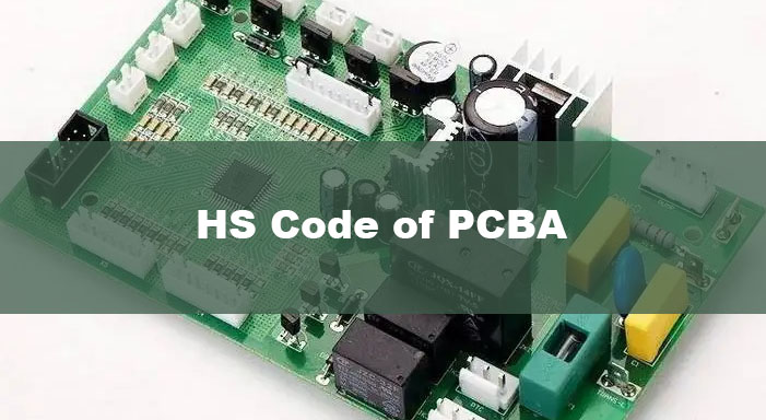
HS code of PCBA is 8543709990

HS code of PCBA is 8543709990

How do you classify printed circuit boards?

According to different classification standards, printed circuit boards can be divided into many types, such as single-sided boards, double-sided boards, multi-layer boards, rigid boards, flexible boards, etc.

The role of HS codes for printed circuit boards

HS codes are a way for customs to classify goods, and are also an important basis for import and export statistics. As an electronic component, printed circuit boards also need to be HS coded so that customs can accurately classify and manage them.

Types of HS codes for printed circuit boards

There are two main HS codes for printed circuit boards: 85340010 and 85340090. Among them, 85340010 is mainly used for printed circuits with more than six layers, while 85340090 is mainly used for printed circuits with four layers or less. The difference between the two codes lies in the number of layers of the printed circuit board, because printed circuits with more than six layers require higher technical requirements and more complex production processes.

How to choose the correct HS code

The specific HS code may vary depending on product specifications, materials and other factors. Therefore, in actual operation, it is recommended to consult relevant departments or professionals according to the specific situation to ensure accuracy. If you are not sure which HS code to choose, you can consult the printed circuit board manufacturer or relevant industry associations for more professional advice.

How do I do a customs declaration?

  1. Declare the code accurately. Select the sub-classification number corresponding to the printed circuit board according to the actual situation to avoid penalties or detention caused by coding errors.
  2. Provide a complete production process. The production process of the printed circuit board needs to be provided in the customs declaration, including the procurement, production, processing, testing and other links of the materials, so as to facilitate the customs inspection of the printed circuit board.
  3. Declare accurate materials and technical parameters. The technical parameters such as the substrate, copper foil thickness, board thickness, drilling diameter, line width, line spacing, etc. used in the printed circuit board need to be accurately declared in the customs declaration.
  4. Re-declaration is required if the dominant production process is changed. If the dominant production process is changed, it is necessary to re-declare to the customs and re-make the customs declaration.
  5. Comply with relevant national quality standards. Printed circuit boards need to meet relevant national quality standards, such as ISO, UL, etc.

hs code electronic,How do I find an HS code?The HS code for PCB (printed circuit board) is 8534001000. PCBs made of FR-4 material (i.e. silicon tetrachloride fiberglass board) are classified under HS code 8534.00.00

You may also like

How to Read Circuit Boards and Schematics?

August 7th, 2024

How to read circuit boards and schematics is a basic skill for anyone interested in electronics. Whether you’re a beginner or a technician, knowing how to read these diagrams is crucial. In this blog, we would like to share the key points and components symbols in the PCB schematics.

How to Understand a PCB Board?

A printed circuit board is a basic of electronic components interconnected via conductive paths printed on a baseboard. We can see it everywhere. They connect and support various components using conductive tracks, pads, and other features. To understand a PCB, start by identifying its main sections: power supply, signal paths, and grounding. Look for the layout patterns, which often follow a logical flow.

Special Types of Circuit Boards

Circuit boards come in various types, each designed for specific applications and processes. Apart from the standard FR4 PCB, metal core PCB, ceramic PCB, rigid-flex PCB, there are some other special PCB uses different process. Here, we’ll explore them based on their unique manufacturing processes, including HDI, busbar, extra thin, IC substrate, high Tg, heavy copper, RF, and impedance control PCBs.

High-Density Interconnect (HDI) PCB

HDI PCBs are designed for compact and complex electronic devices. They feature higher wiring density per unit area compared to traditional PCBs. The process involves microvias, buried vias, and blind vias to create intricate pathways. HDI technology allows for more components on a smaller board, enhancing performance and reducing size. This type of PCB is commonly used in smartphones, tablets, and other high-tech gadgets. The HDI PCBs that EBest Circuit (Best Technology) can make is:

  • 1+N+1
  • 2+N+2
  • 3+N+3

Busbar PCB

Busbar PCBs are specialized boards that handle high current loads efficiently. It belongs to the heavy copper PCB. They use thick copper layers to conduct electricity with minimal resistance. The busbar process involves integrating these thick copper bars within the PCB to distribute power uniformly. They are mainly used in the electric vehicles, power supplies and industrial machinery.

Extra Thin PCB

Extra thin PCBs are designed for applications where space and weight are critical constraints. These boards can be as thin as 0.2mm, allowing them to fit into slim devices like wearables and medical implants. The manufacturing process focuses on using thinner materials and precision etching techniques to achieve the desired thickness without compromising functionality.

IC Substrate PCB

IC substrate PCBs act as the base for integrated circuits (IC). They provide interconnections between the IC and the PCB. These PCBs are crucial in devices like processors, memory modules, and graphic cards, where precision and reliability are paramount.

High Tg PCB

High Tg (glass transition temperature) PCBs are designed to withstand higher temperatures. The Tg value indicates the temperature at which the PCB material transitions from a rigid to a soft state. High Tg PCBs use materials that has over 170 Tg value. So, they are widely used in automotive, aerospace, and industrial applications.

Heavy Copper PCB

Heavy copper PCBs feature significantly thicker copper layers compared to standard PCBs. The process involves plating additional copper to achieve thicknesses of 3oz/ft² or more. These boards handle high currents and thermal cycles, making them ideal for power electronics, motor controllers, and high-power distribution systems.

Radio Frequency (RF) PCB

RF PCBs are designed for high-frequency applications. They use special materials like PTFE (Teflon) to minimize signal loss and interference. This kind of PCB always requires precise control over dielectric thickness and conductor widths to make sure optimal signal integrity. RF PCBs are essential in communication devices, radar systems, and microwave equipment.

What Do the Numbers on a Circuit Boards Mean?

Numbers and letters on a circuit board represent component values, reference designators, and sometimes manufacturing codes. Reference designators (like R for resistors, C for capacitors) help identify each component. The numbers often indicate the order of placement or specific values (e.g., R1, R2 for the first and second resistors).

In addition, some designers prefer to design series number on the PCB board, like 202400001…202400002. For this kind of numbers, they are always aim to easy identification during the assembly or testing.

How to Read Circuit Boards?

Reading a circuit board involves several steps. First, familiarize yourself with the board’s layout and components. Identify key parts such as the microcontroller, resistors, capacitors, and connectors. Trace the pathways or traces to understand the connections. Use the reference designators to match components with their schematic symbols.

Electronic symbols follow standardized guidelines to ensure consistency. The most common standards include IEEE, IEC, and ANSI. These symbols represent various components like resistors, capacitors, diodes, and transistors.

  1. VCC – the positive power supply.
  2. GND – ground or negative power supply.
  3. R – resistor.
  4. C – capacitor.
  5. L – inductor.
  6. Q – transistor or field-effect transistor (FET).
  7. JP – connector or plug/socket.
  8. IC – integrated circuit or chip.
  9. + / – – input/output terminals of a signal.
  10. NC – no connection or an unused pin.

How Do You Read a Circuit Schematic for Beginners?

Read circuit diagram drawings can be consulted by experienced masters. Generally, the first look when reading a circuit schematic is look at the main loop. And then look at the control loop, the control loop requirements are from top to bottom or from left to right. The circuit diagram mainly consists of four parts: component symbol, connection, node and comment/note.

1. Component Symbols

These represent the actual components in the circuit. Their shapes may not resemble the actual components and can even be completely different. However, they generally indicate the characteristics of the components, and the number of pins matches the actual components.

2. Connections

These represent the wires in the actual circuit. While they appear as lines in the schematic, they are often not lines but various shapes of copper foil blocks on commonly used printed circuit boards (PCBs). For example, many connections in a radio schematic may not be line-shaped on the PCB but rather in specific shapes of copper film.

3. Nodes

These indicate the connections between multiple component pins or wires. All component pins and wires connected to a node are conductive, regardless of the number.

4. Comment/note

These are very important in a schematic. All the text in the schematic can be classified as notes. A close look at the schematics reveals annotations everywhere, used to indicate component models, names, and other information.

EBest Circuit (Best Technology) offer top-quality advanced PCB boards, from prototypes to mass production. Our range includes FR4 PCBs of any Tg, FPC, ceramic PCBs, aluminum PCBs, Teflon PCBs, and copper-base PCBs. Every product and service is traceable and verified with ISO, IATF, RoHS, UL, and REACH certifications. Enjoy free samples for bulk orders, complimentary functional testing, and fast delivery.

You may also like

What is Tda7294 amplifier board &tda7294 datasheet

August 7th, 2024

TDA7294 is a class AB monolithic audio amplifier integrated circuit launched by SGS-THOMSON Microelectronics in the 1990s. It swept away the raw, cold and hard sound of previous linear integrated amplifiers and thick film integrated amplifiers, and is widely used in HiFi fields, such as home theaters, active speakers, high-performance TVs and other fields.

The chip adopts a 15-pin dual-row asymmetric plug-in package, the differential input stage is composed of bipolar transistors, and the driver stage and power output stage use DMOS field-effect transistor semiconductor technology. This hybrid semiconductor manufacturing process allows TDA7294 to take into account the advantages of bipolar signal processing circuits and MOS power tubes, and the playback sound is very friendly (it is praised by audiophiles as a “tube-flavored amplifier”); the built-in silent standby function, short-circuit current and overheating protection functions make its performance more perfect. It can be used in HiFi home audio, active audio, high-performance TVs and other fields.

Tda7294 amplifier board

tda7294 amplifier board

tda7294 amplifier board PCBA

  1. This circuit is an official standard circuit, stable and reliable.
  2. The filter uses a large electrolytic capacitor with a withstand voltage of 50V and a capacity of 2200uf.
  3. Power supply voltage: dual 12-36V ring transformer, dual 32V ring transformer is recommended
  4. Output power: 85W*1 undistorted rated power, peak power 100W
  5. Can easily drive speakers above 100W, speaker impedance: 4-8 ohms
  6. PCB size: 50*50mm
tda7294 amplifier board

Basic parameters:
Power supply: dual 18-28V AC
Power: 2X80W+160W subwoofer
Circuit board size: 218x98MM
Potentiometer function: low frequency frequency adjustment, subwoofer volume. Left and right channel volume, treble, bass.

Adopting the new laser dark word TDA7294
The power filter uses 6 63V3300UF capacitors, and the rectifier uses a 25A imported rectifier flat bridge.
PCB uses 1.6mm thick double-sided board, 2.0 ounces copper thickness, and full tin spraying process to ensure good passing performance of large and small currents.
Fever component assembly, the subwoofer part consists of two new TDA7294 BTL output,
The low-pass filter is designed according to the frequency adjustable design of home theater style (50-150HZ), with strong power!
The left and right channels are served by two TDA7294 respectively, and the input coupling capacitor uses the German imported WIMA 2.2UF coupling capacitor, which makes the sound sweeter!
The signal-to-noise ratio of the board is also very high, and even if you put your ear close to the speaker, you can’t hear the AC noise! ​​It is the best choice for upgrading 2.1 amplifiers!

TDA7294 datasheet

TDA7294 datasheet
TDA7294 datasheet

TDA7294 Main Features

Wide supply voltage range: ±10V ~±40V
High output power: 70W (up to 100W)
Standby and mute functions
Noiseless ON/OFF switch
Low noise and low distortion
Short circuit protection and overheat protection

TDA7294

Pin function
Pin 1 is the standby terminal;
Pin 2 is the inverting input terminal;
Pin 3 is the positive input terminal;
Pin 4 is grounded;
Pins 5, 11, and 12 are empty pins;
Pin 6 is the bootstrap terminal;
Pin 7 is +Vs (signal processing part);
Pin 8 is -Vs (signal processing part);
Pin 9 is the standby pin;
Pin 10 is the mute pin;
Pin 13 is +Vs (final stage);
Pin 14 is the output terminal;
Pin 15 is -Vs (final stage)

DIY Production

1) The first step is to get the PCB. Here you can make the PCB yourself by DIY ironing method. Since the PCB is easy to make, the PCB design is kept single layer only, or you can get ready-made quality PCB from best.or custom tda7294 amplifier board.
2) After the PCB is completed, carefully mount all small components like jumpers, resistors, diodes, etc. to the PCB and trim their terminals, then solder them to the PCB first, because there are many components on this board, so it is better to solder them one by one
3) After installing the small components, install the large components like capacitors, fuse holders, rectifiers to the PCB and solder them. (Don’t install the power filter capacitor, 22000uF capacitor for now. Completed in the following steps)
4) After that, it’s time to mount all 7 ICs to the PCB and solder them.
5) Now properly mount the heat sink on the IC using insulating MICA and insulating plastic shoulder washers. Remember to use good quality thermal paste between the heat sink and IC.
6) After mounting the IC on the heat sink. Check the continuity between the heat sink and the IC back plate using a multimeter. There should not be any continuity between them. Please note the heat sink isolation
7) Now mount the cooling fan to the PCB using cable ties or any other suitable method.
The board assembly is now complete. Clean the track side of the board using IPA (Isopropyl Alcohol) or cleaning flux and then power the board using a 20-0-20 VAC transformer or a 24-0-24 VAC transformer.

Which one has better sound quality, TDA7294 or LM3886? Voltage AC 28v

LM3886 has better bass because its maximum current can reach 10A, which means it can drive a 2-ohm box without any problems. From the parameters alone, LM3886 is worse than 7294. And it is true in practice, especially for bass. If the transformer is OK, it feels very powerful. 7294 is not as good as 3886 in bass. The current is large when it comes to bass. 7294 itself has overcurrent protection. When the current reaches a certain level, it starts to limit the output current. However, 7294 is better in treble.

You may also like

How to Check PCB with a Multimeter?

August 5th, 2024

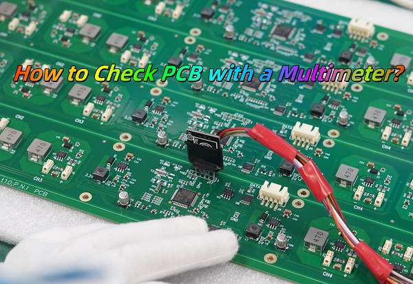
Common PCB failures are mainly concentrated on components such as capacitors, resistors, inductors, diodes, transistors, MOSFETs, integrated chips (IC), and crystals. Some obvious damages can be visually detected, while others require the use of tools. Today, let’s learn how to troubleshoot PCB faults using a multimeter.

How to Check PCB with a Multimeter?

How Will You Diagnose a Faulty PCB By Visually?

For some printed circuit boards, we can check by our naked eyes. Here are some common ways to follow:

1. Check the condition of components

When you get a faulty PCB, first observe if there are any obvious component damages, such as burnt or swollen electrolytic capacitors, burnt resistors, and damaged power devices.

2. Inspect the soldering of the PCB

Check if the printed circuit board (PCB) is deformed or warped; if there are any loose or poorly soldered joints; if the copper cladding on the PCB is lifted, burnt, or blackened.

3. Examine the component plug-ins

Ensure the correct orientation of integrated circuits, diodes, and the PCB power transformer.

How to Check PCB with a Multimeter?

Before you start testing your PCB, ensure you have the right tools and environment. Here’s a checklist to get you started:

1. Safety First: Wear anti-static gloves and ensure you are working on an anti-static mat to prevent damage to the PCB.

2. Multimeter Selection: Choose a multimeter with the ability to measure voltage, resistance, and continuity. A digital multimeter is preferred for accuracy.

3. Visual Inspection: Examine the PCB for visible signs of damage such as burnt components, broken traces, or solder bridges.

4. Power Off the Board: Always test the PCB with the power off to avoid any electrical hazards and damage to the multimeter.

How Do You Test Individual Components on a PCB?

Testing individual components like resistors, capacitors, and diodes can pinpoint the exact failure. Here’s a general approach:

  • Diode
  • Transistor
  • MOSFET
  • Electrolytic Capacitors

How to Test Diodes?

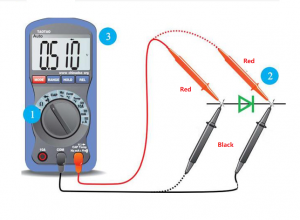
1. Set the MF47-type multimeter to measure resistance.

2. Place the red and black probes on the two ends of the diode and read the value.

3. Swap the probes and measure again.

4. Judge based on the two measurements: the forward resistance of small power germanium diodes is 300-500Ω, silicon diodes are about 1kΩ or larger. The reverse resistance of germanium diodes is tens of kilo-ohms, and silicon diodes are above 500kΩ (values are much smaller for high-power diodes). A good diode has low forward resistance and high reverse resistance, and the larger the difference, the better.

How to Check PCB with a Multimeter?

5. If both forward and reverse resistances are very low, the diode is short-circuited; if both are very high or infinite, the diode is open-circuited and needs to be discarded.

How to Test Transistors?

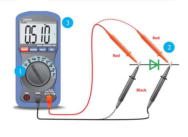
1. Set the digital multimeter to the diode mode.

2. Measure the PN junction with the probes. If it conducts forward, the displayed value is the forward voltage drop of the PN junction.

3. Determine the collector and emitter: measure the forward voltage drop of the two PN junctions, the larger drop is the emitter (e), and the smaller drop is the collector (c). If the red probe is connected to the common terminal, the transistor is NPN type, and the common terminal is the base (b); if the black probe is connected to the common terminal, the transistor is PNP type, and the common terminal is the base (b).

4. For in-circuit testing, measure the forward and reverse resistance of the PN junction to determine if the transistor is damaged. If the branch resistance is larger than the forward resistance of the PN junction, there should be a clear difference between the forward and reverse resistances, otherwise, the PN junction is damaged.

How to Check PCB with a Multimeter?

The Way to Test MOSFETs?

1. Connect the black probe to the drain (D) and the red probe to the source (S), the resistance should be 500-600.

2. Without moving the black probe, touch the gate (G) with the red probe, then measure the source (S) again; it should conduct.

3. Connect the red probe to the drain (D), touch the gate (G) with the black probe, then measure the source (S); the resistance should be the same as the first measurement, indicating the MOSFET is working normally.

How to Test Electrolytic Capacitors?

1. Select the appropriate range on the MF47-type multimeter based on the capacitor’s capacity. Use RƗ1K range for capacitors below 47μF, and RƗ100 range for those above 47μF.

2. Connect the red probe to the negative lead and the black probe to the positive lead of the capacitor.

3. On initial contact, the multimeter needle will deflect right and then gradually return to the left until it stops at a certain position (close to infinity). This value is the capacitor’s forward leakage resistance; the larger the value, the better the capacitor’s performance.

4. Swap the probes and repeat the process. The measured value will be the reverse leakage resistance, slightly smaller than the forward leakage resistance.

5. If no charging phenomenon occurs (the needle doesn’t move), the capacitor is either open or short-circuited internally. If the resistance is very small or zero, the capacitor is leaky or has broken down and cannot be used.

This is the end of this article, if you want to know more about it, welcome to contact us.

You may also like

How to Clean Flux Off PCB? – EBest Circuit (Best Technology)

July 31st, 2024

Flux is usually a mixture of rosin as the main component and is an auxiliary material to ensure the smooth progress of the PCB soldering process. Soldering is the main process of PCB assembly, flux is the auxiliary material used in soldering. The main function of flux is to remove the oxide of the solder and the base metal surface to be welded, so that the metal surface to achieve the necessary cleanliness.

Flux prevents the reoxidation of the surface during welding, reduces the surface tension of the solder, and improves the welding performance. The performance of flux directly affects the quality of electronic products. There are different types of solder paste flux, including rosin-based, water-soluble, and no-clean flux. Each has its specific applications and cleaning methods.

Types of Flux

  • Rosin Flux

This is one of the most commonly used fluxes in soldering. It includes activated rosin flux (RMA), which contains additional chemicals for enhanced cleaning of oxides, and non-activated rosin flux (RA), which offers basic cleaning for general purposes. Rosin flux is effective at preventing oxidation and improving solder flow, making it suitable for a wide range of electronic soldering applications.

  • Water-Soluble Flux

This type of flux uses water-soluble chemicals to provide strong cleaning action. It is easily removed with water, making it ideal for applications where thorough residue removal is necessary. Water-soluble flux is often used in automated soldering processes where post-soldering cleanup is a key concern.

  • No-Clean Flux

Designed to leave minimal, non-corrosive residue, no-clean flux does not require cleaning after soldering. This type of flux is beneficial in situations where cleaning is difficult or impractical, as it reduces post-soldering processing time while ensuring that the residue does not affect the performance of the PCB.

  • Organic Acid Flux

Contains organic acids like citric or formic acid, providing effective cleaning and fluxing. While it offers strong fluxing action, it is more corrosive compared to rosin fluxes. Organic acid flux is used in applications requiring robust cleaning, with careful consideration of the corrosion risk.

  • Solder Paste Flux

This flux is a combination of flux and solder powder, used in reflow soldering processes. It is commonly employed in surface-mount technology (SMT), where the paste is applied to PCB pads before component placement and reflow. Solder paste flux streamlines the soldering process by integrating fluxing and soldering into one step.

Is it Bad to Leave Flux on PCB?

There is obvious that leaving flux residue on a PCB surface can lead to several issues. Flux residues can attract moisture, resulting in corrosion of metal traces and component leads, which can compromise the integrity of the PCB over time. Some flux residues are conductive, potentially causing short circuits and affecting signal integrity, especially in high-frequency applications. Even no-clean flux can leave residues that impact sensitive components. Cleaning flux off the PCB can make sure the optimal performance and reliability of the overall product.

How to Remove Flux After Soldering?

We know leaving the flux on the PCBA surface is not a good thing, so how to remove it? Here we listing some common methods that manufacturers will used after soldering. Hope this information is helpful for you!

  • Isopropyl Alcohol (IPA)

Use high-purity IPA (90% or higher). Apply it to the flux residue with a brush or cotton swab, gently scrubbing the area to dissolve the flux. IPA evaporates quickly and is effective for most flux types.

  • Water Washing

Water washing is a common and straightforward cleaning method. It uses pure or deionized water to remove flux residues. This technique is simple, cost-effective, and easy to implement. However, water washing can potentially harm some PCBs and components if moisture accumulates on pads and pins, leading to short circuits or corrosion.

  • Solvent Cleaning

Solvent cleaning is an efficient method that dissolves flux residues using chemical solvents. The solvent is then rinsed or sprayed off to clear the flux. While this method provides rapid and effective cleaning, solvents can be costly and require careful handling due to their chemical properties and safety considerations.

  • Ion Cleaning

Ion cleaning is a high-tech approach that uses ion beams to clean the surface of PCBs. The high-energy and high-speed ion beams effectively remove contaminants and flux residues without damaging the PCB or components. However, ion cleaning equipment is expensive and requires specialized technology and support.

  • Oxidation Cleaning

Oxidation cleaning is a physical cleaning method where oxidizing agents convert flux residues into easily removable substances. This technique is suitable for PCBs and components that are not compatible with water or solvent cleaning. The cost of oxidizing agents can be high, and safety precautions are necessary due to their reactive nature.

  • Dry Ice Cleaning

Dry ice cleaning uses CO2 dry ice pellets as the cleaning medium. This method is efficient, environmentally friendly, and does not produce secondary pollution. During cleaning, high-speed CO2 dry ice pellets impact the flux residues on the PCB surface. The extremely low temperature of the dry ice causes the flux residues to become brittle, allowing them to be easily removed without damaging the PCB. This method offers a thorough cleaning solution while preserving the integrity of the circuit board.

FAQs

1. Can I use vinegar to clean flux off a PCB?

Vinegar can be used to clean certain types of flux, but it’s not as effective as IPA or specialized flux removers. It’s best to use a solvent designed for flux removal.

2. How often should I clean my PCB?

Clean your PCB after every soldering session to prevent residue buildup and ensure optimal performance.

3. Is it safe to use a hairdryer to dry a PCB after cleaning?

Yes, but use the lowest heat setting to avoid damaging sensitive components. Ensure the PCB is completely dry before powering it on.

4. Can I use a toothbrush for cleaning flux?

A toothbrush can be used, but a brush with anti-static properties is recommended to prevent static damage to the PCB.

5. Is no-clean flux really safe to leave on a PCB?

While designed to be left on, no-clean flux can still leave residues that may affect sensitive components. It’s best to clean it off for maximum reliability.

All in all, cleaning flux off your PCB is a crucial step to keep the reliability of your product. Remember, a clean PCB is a reliable PCB. Choose the right solvent, follow proper cleaning techniques, and your electronics will thank you with years of flawless performance.

For high-quality PCB & PCBA solutions and expert advice, choose EBest Circuit (Best Technology). We have more than 18 years in this field. Our commitment to excellence ensures your projects are in good hands. Contact us today to learn more about our products and services.

You may also like

Dry Soldering: How to Prevent and Fix Dry Solder Joint?

July 25th, 2024

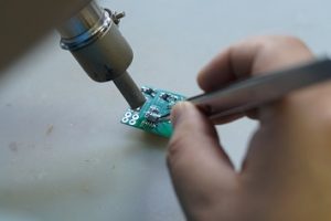
It’s essential to ensure that solder joints are made correctly in any electronics construction. Poor and dry soldering cause equipment not to work once. Or there is a possibility that the solder joint could fail. In this blog, we will introduce why dry soldering occurs and how to solve it.

What is Meant by Dry Soldering?

Dry soldering refers to a poor solder joint that lacks proper electrical connectivity on a PCB assembly product. This issue occurs when the solder does not properly melt and bond to the components, leading to weak connections. These joints are often brittle and prone to failure, which can result in intermittent or complete loss of electrical connectivity.

Dry Soldering: How to Prevent and Fix Dry Solder Joint?

Why Dry Solder Joint Causes?

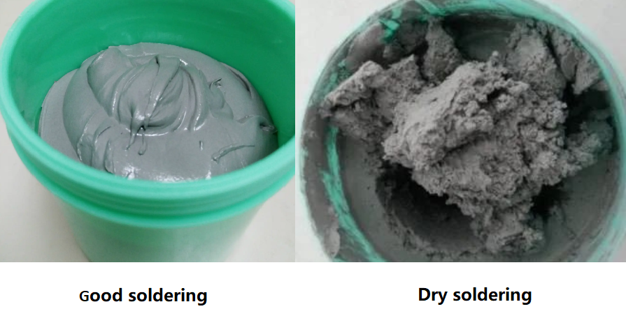
Dry solder joints occur due to several reasons, each impacting the quality of the solder connection. First of all, the solder paste reflow process is only a small area, which is easier to harden than the solder paste in the solder paste can. At this time, the solder paste will not melt, and the flux cannot cover the solder joint, resulting in poor welding of the solder joint. Meanwhile, the solder paste is easier to heat transfer, and the high temperature actually makes the solder paste not easy to melt, so we can slightly adjust the reflow welding temperature curve to solve the problem, or welding in a nitrogen environment is basically a good way to solve this problem.

Secondly, the solder paste does not melt because its own composition contains a very volatile flux, which is also the reason why the solder paste is easy to harden. Among them, the flux with the largest content of solder paste is rosin, rosin contains a lot of rosin acid, rosin acid is easy to lose activity at too high temperature. Therefore, the temperature of the welding process should be controlled to ensure that the temperature is about 200 ° C, which is not suitable for too high or too low. At the same time, the quality of thixotropic agent will also lead to the solder paste is easy to dry, the quality of thixotropic agent is not good will affect the viscosity of the solder paste, the viscosity of the solder paste is easy to dry. Therefore, the choice of high-quality solder paste can fundamentally solve the problem that the solder paste is easy to harden.

In addition, the use of solder paste scene, humidity, temperature and other external factors will also affect the solder paste in the use of hard non-melting phenomenon. So these external factors should be paid attention to. I hope these solutions can solve your problems.

How Do You Fix Dry Solder?

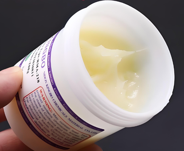
Solder paste is one of the very important materials in the electronics industry, and it has an important impact on the production quality of the entire component. Here are some tips that can help to fix the dry solder paste.

1.Add flux

              Usually, if the solder paste is too dry, you can try to add some water to the right amount of flux, stir well and add it to the solder paste. This can play a certain role in alleviating drying and improve the fluidity of the solder paste.

              Dry Soldering: How to Prevent and Fix Dry Solder Joint?

              2. Take some measurements during management

                a. Keep the ambient temperature moderate during storage;

                b. Stir well before use;

                c. Cover the solder paste in time after welding to avoid exposure to the air.

                3. Replace it with new one

                If the solder paste becomes too dry, adding flux is difficult to restore its original properties, it is recommended to replace the solder paste to avoid affecting the quality of the components.

                Therefore, we need to regularly maintain and manage the solder paste to ensure that its quality meets the standard requirements.

                What Does a Dry Solder Look Like?

                Recognizing a dry solder joint is crucial for proper diagnosis and repair. Unlike a good solder joint, which is shiny and smooth, a dry joint looks matte and rough. The joint might have visible cracks or look brittle. It might not be fully bonded to the component lead or the PCB pad. Identifying these visual cues can help in quickly addressing the issue.

                How Do You Prevent Dry Solder?

                Preventing dry solder joints is key to maintaining the reliability of your electronic projects. You can try to use these tips to prevent your solder paste become dry.

                • Proper heating
                • Clean surfaces
                • Use quality solder
                • Steady hand
                • Maintain equipment
                • Fast usage and storage

                If you want to know more about solutions of dry solder paste, you can read our another post, How to Solve Dry Solder Paste.

                How to Tell If Solder is Bad?

                Bad solder can lead to dry joints and other issues. So, how can we identify if my solder paste is bad? May you can follow these points. If everything matches up, there’s no doubt that your solder paste is broken.

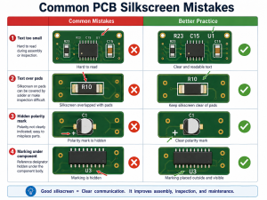
                • Appearance of solder joints

                Bad solder joints often appear dull or matte instead of shiny and smooth. They may also show cracks or a brittle texture, indicating poor bonding or excessive heating. These visual signs suggest that the solder did not properly melt or flow.
                Dry Soldering: How to Prevent and Fix Dry Solder Joint?
                • Solder flow and coverage

                If the solder does not adequately cover the component leads or PCB pads, or if it spreads unevenly, it is likely bad. Proper soldering should result in a well-formed, consistent fillet around the leads, ensuring reliable electrical connections.

                • Difficulty in melting

                Solder that requires unusually high temperatures or takes a long time to melt may be old or contaminated. Proper solder should melt easily at the recommended temperature and flow smoothly to create a solid joint.

                • Contamination indicators

                Oxidized or tarnished solder indicates contamination and can affect its performance. Excessive residue or debris also points to poor quality, affecting how well the solder adheres and flows.

                EBest Circuit (Best Technology) is a one-stop PCB manufacture and PCBA service provider, our SMT factory is equipped with more than 6 assembly lines. Meanwhile, we have automatic SPI machine and solder paste printing machine, with good management system, we can ensure the good quality of solder paste. In addition, there are many advanced equipment in our workshop, including online dual AOI, X-ray, Nitrogen reflow oven, dry-ice cleaning machine, and so on.

                Trust us, we are the one of most reliable PCBA manufacturer in China and Vietnam. Contact us for more.

                You may also like

                PCB vs CCA: What is a Circuit Card Assembly?

                July 22nd, 2024

                Hey there! If you’re curious about circuit card assembly (CCAs) and what makes them tick, you’ve come to the right place. CCAs are the unsung heroes behind many of the electronic devices we use every day. Let’s dive into what they are, their essential parts, how they’re made, and why they’re so important.

                What is a circuit card assembly?

                Circuit card assembly or CCA is the process of producing printed circuit boards. In essence, it is the same as PCBA (PCB assembly), just in different name. CCA is a manufacturing technology that converts raw materials into printed circuit boards. It is used in many industries, including the military and aerospace sectors. This type of manufacturing requires skilled professionals to lay out the design and then assemble it. If you are planning to buy a batch of circuit card components, here are some things you should know about CCA.

                PCB vs CCA: What is a Circuit Card Assembly?

                A circuit card is a thin, flat dielectric material on which conductive paths or traces are etched. These paths connect various electronic components. They are also used to connect components to sockets on printed circuit boards. Circuit card assy is the process of manufacturing circuit card components. The process involves adding electronic components to the substrate.

                Key components of a circuit card assembly (CCA)

                Circuit card assembly have several key components to make the circuit function properly. These can be divided into three basic components.

                • Printed Circuit Board (PCB)
                • Electronic component
                • Solder paste
                • Printed Circuit Board (PCB)

                This is the backbone of the CCA. The printed circuit board provides the structural foundation on which all other components are mounted. A PCB is typically made of a flat, insulating material such as FR4 fiberglass, which is layered with conductive tracks made of copper. These tracks form the circuit pathways that connect various electronic components. The PCB board can be single-sided, with components and conductive tracks on one side only, or double-sided, with tracks and components on both sides. For more complex applications, multi-layer PCBs are used, which consist of multiple layers of insulating material and conductive pathways stacked together. These printed circuit boards are essential in ensuring that electrical signals are routed efficiently and reliably across the assembly.

                PCB vs CCA: What is a Circuit Card Assembly?

                • Electronic Components

                These include resistors, capacitors, integrated circuits, transistors, and more passive and positive components. Each part plays a specific role in the circuit, like pieces of a puzzle fitting together to make a complete picture. Resistors control the flow of electrical current, capacitors store and release energy, integrated circuits (ICs) perform various functions like processing and memory storage, and transistors act as switches or amplifiers. These components are carefully placed on the PCB in positions that allow them to connect and interact as designed.

                PCB vs CCA: What is a Circuit Card Assembly?

                • Solder paste

                Solder paste is like the glue that holds everything together, but it’s electrically conductive. It’s used to attach the electronic components to the PCB, so that they can stay put and work properly. Soldering creates a strong, conductive bond between the component leads and the PCB’s copper tracks. There are different types of soldering, such as lead-based and lead-free solders, each with its specific properties and applications. The soldering process can be done manually or using automated printing machines, depending on the complexity and volume of the assembly. Please noticed that solder paste should used in a very short time, otherwise, it will become dry solder paste.

                PCB vs CCA: What is a Circuit Card Assembly?

                What is the Difference Between a PCB and a CCA?

                You might wonder, what’s the difference between a PCB and a CCA? Well, here’s a quick rundown:

                AspectPCB (Printed Circuit Board)CCA (Circuit Card Assembly)
                DefinitionA blank board with conductive pathwaysA PCB populated with electronic components
                ComponentsNo electronic componentsIncludes electronic components like resistors, capacitors, ICs
                FunctionalityServes as the foundation for electronic circuitsA functional electronic circuit ready for use in devices
                Manufacturing StepsInvolves design, etching, and printing of conductive pathsInvolves PCB manufacturing plus component placement and soldering
                Usage StageIntermediate stage in manufacturingFinal stage, ready for integration into electronic devices
                ComplexityLess complex, involves fewer manufacturing stepsMore complex, involves multiple stages of assembly and testing

                What is the circuit card assembly manufacturing process?

                Making a CCA is a multi-step process:

                Design

                First, the PCB layout is designed using computer software. It includes numerous steps, like schematic drawing, layout design, SI, PI analysis, DFM. This can ensure the PCB board can fit all the necessary components and function correctly.

                Fabrication

                The PCB is then fabricated, which involves creating the physical board with layers of insulating and conductive materials. This is where the board gets its pathways. In this step, proceed strict quality control process to make sure the bare boards are qualified.

                Component Placement

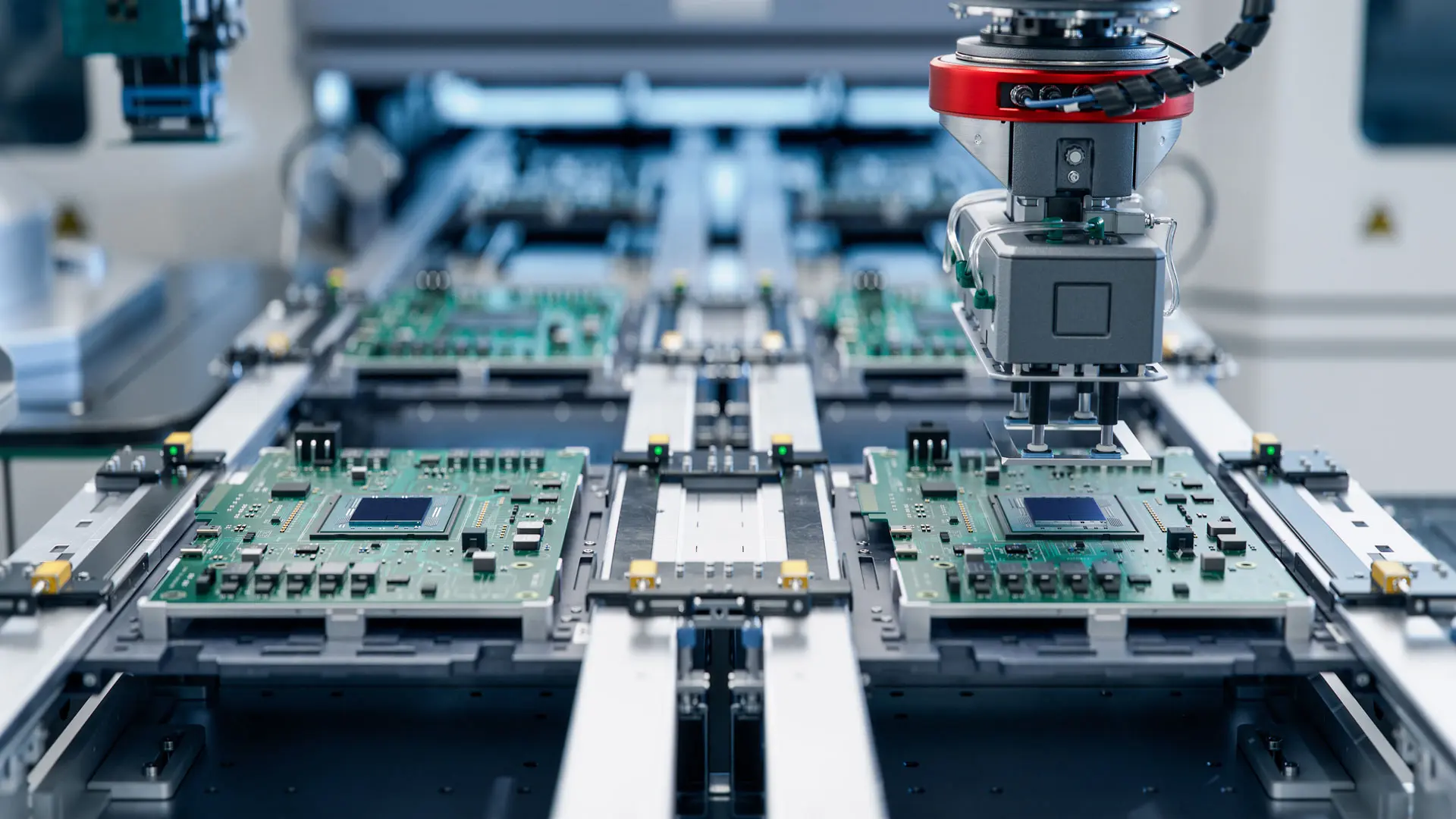
                Next, printing solder paste and preparing components, then place them onto the PCB board according to the BOM file (bill of material). After setting up the pick and place machine, automated machines can precisely position each component based on the design.

                Soldering

                The components are soldered to the PCB. This can be done using methods like wave soldering or reflow soldering to ensure everything is securely attached and electrically connected. You must know, different products require different parameters, please make sure all the parameters like temperatures, time are suitable.

                Inspection and Testing

                The assembled CCA goes through rigorous inspection and testing to ensure it works as intended. This includes visual inspections, automated optical inspections (AOI), in-circuit testing (ICT), aging testing and functional testing.
                Final Assembly

                If the CCA passes all tests, it moves on to final assembly, where it’s integrated into the larger electronic system or device. That is we say the box building assembly.
                What are the types of circuit card assembly?

                CCAs can be divided into various types according to the different manufacturing technology.

                Through-Hole Technology (THT) Assembly

                Here, components have leads or pins inserted into holes drilled through the PCB and soldered on the other side. This method provides strong mechanical bonds, making it great for components that experience mechanical stress. It’s often used in aerospace, military, and industrial equipment.

                Surface Mount Technology (SMT) Assembly

                In SMT, components are mounted directly onto the PCB surface using solder paste. No drilling required, which allows for higher component density and smaller PCBs. This method is commonly used in consumer electronics, telecommunications, and automotive industries.

                Box Building Assembly

                Box building assembly involves the complete assembly of electronic systems, including CCAs, into enclosures or boxes. This process includes not only the assembly of the PCB but also the integration of cables, connectors, and other components into a final product. Box building is ideal for producing complete electronic devices ready for end-use.

                Advanced materials for CCAs

                Advanced materials help CCAs perform better and last longer:

                • High-Temperature Laminates (e.g., FR-4, Polyimide)

                High temperature laminate like FR4 or polyimide. These materials can handle extreme conditions without breaking down. FR-4 is popular for its excellent thermal and mechanical properties, while polyimide is great for high-temperature stability.

                • Flexible Substrates (e.g., Kapton, PET)

                Kapton and PET are the most common flexible substrate. These materials allow CCAs to bend and flex. Kapton, a type of polyimide, is known for its high thermal resistance and flexibility, making it perfect for wearable electronics and medical devices. PET (polyethylene terephthalate) is another flexible material with good electrical insulation properties.

                • Advanced Solder Compounds

                SAC305 (a lead-free alloy of tin, silver, and copper) is favored for its mechanical and thermal properties. Whatever you want to mount a ceramic PCB or the flexible PCB, it is the best choice. Sn63Pb37, a traditional tin-lead solder, is still used for its ease of use and excellent performance.

                Reliable circuit card assembly manufacturers

                Choosing the right manufacturer for your CCAs is key to getting quality products. PCBonline and EBest Circuit (Best Technology) are go-to-choice reliable circuit card assembly manufacturers. Both of them has advanced pick and place machine, full-auto SPI, AOI equipment, ensuring a good quality.

                As a leading manufacturer in the circuit card assembly, EBest Circuit (Best Technology) prides full turn-key service, ranging from the PCB design, PCB fabricating, electronic component sourcing, circuit card assembly and box build assembly. We handle complex and high-volume orders efficiently, ensuring timely and fast delivery without sacrificing quality. In 2023 alone, we completed over 5000 high-complexity projects with a client satisfaction rate of over 98%.

                It is crucial for anyone to fullly understand the circuit card assembly in the electronics industry. From their basic components and manufacturing process to the advanced materials used, CCAs are the backbone of modern electronic devices.

                You may also like