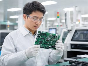
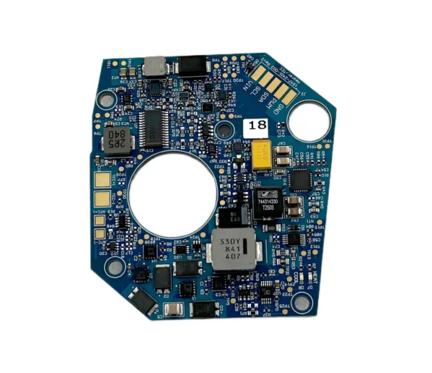
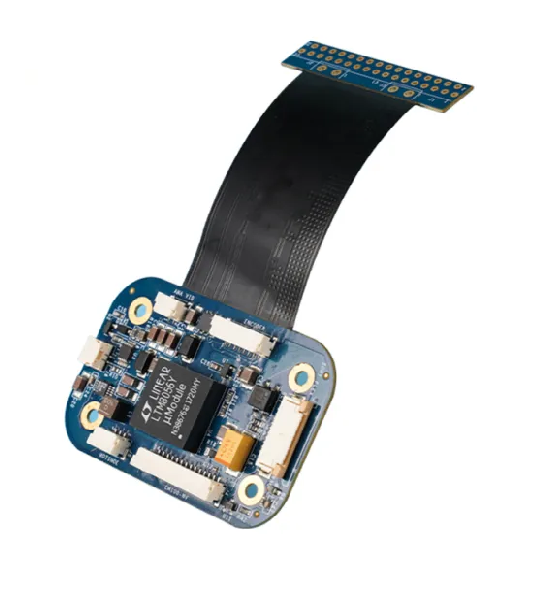
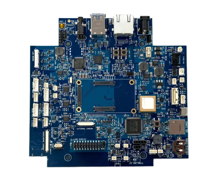
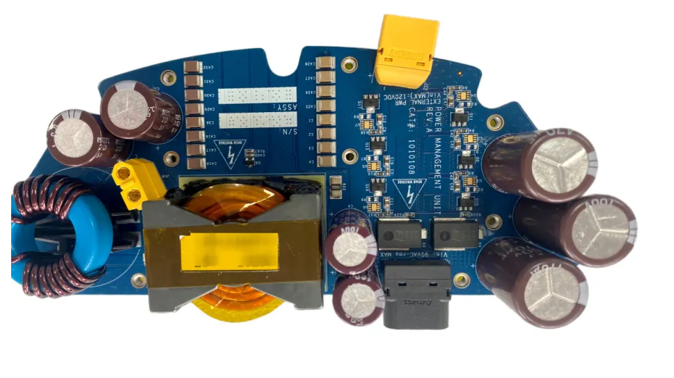
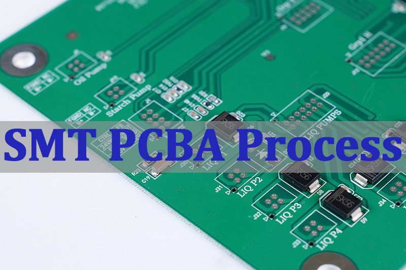
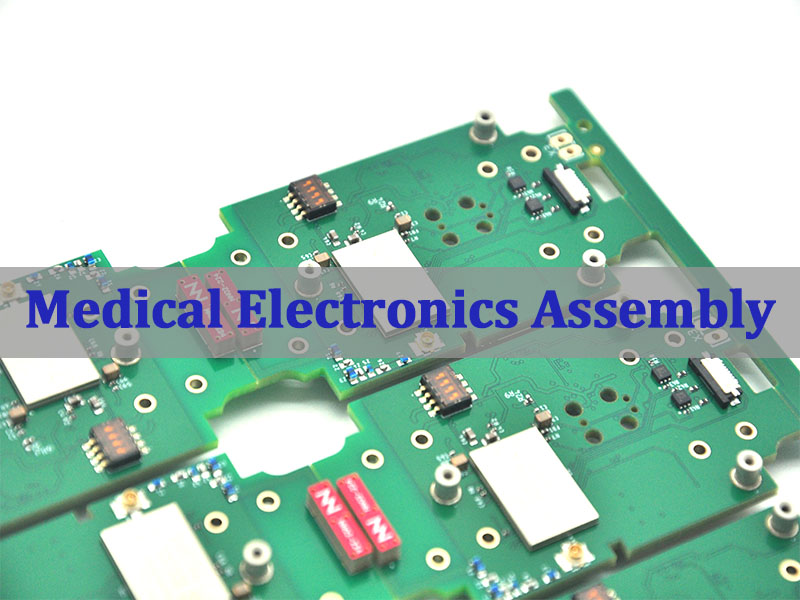
PCBA manufacturing converts a bare printed circuit board into a functional electronic assembly. The process usually combines component sourcing, solder paste printing, automated placement, reflow soldering, through-hole assembly, inspection, programming, and electrical testing.
Component placement is only one part of the job. The larger risks often come from incorrect file revisions, unavailable parts, unsuitable footprints, weak test coverage, soldering defects, and unclear responsibility between the PCB fabricator and assembly provider.
A well-managed PCBA project therefore starts with complete production data and a clear definition of quality, testing, traceability, and delivery requirements.
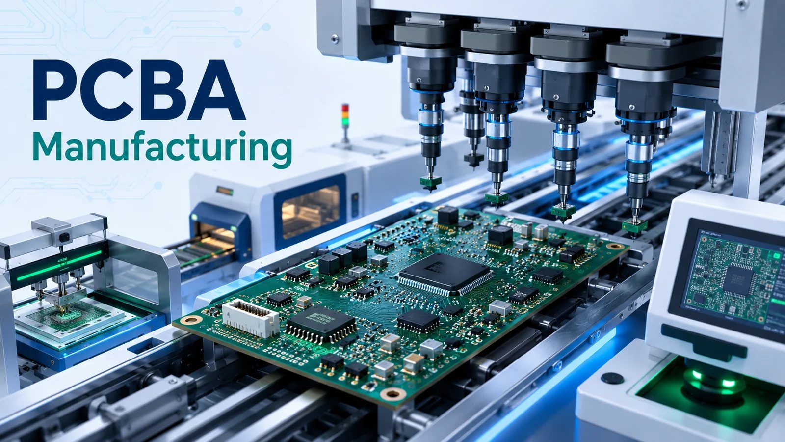
What Is PCBA Manufacturing?
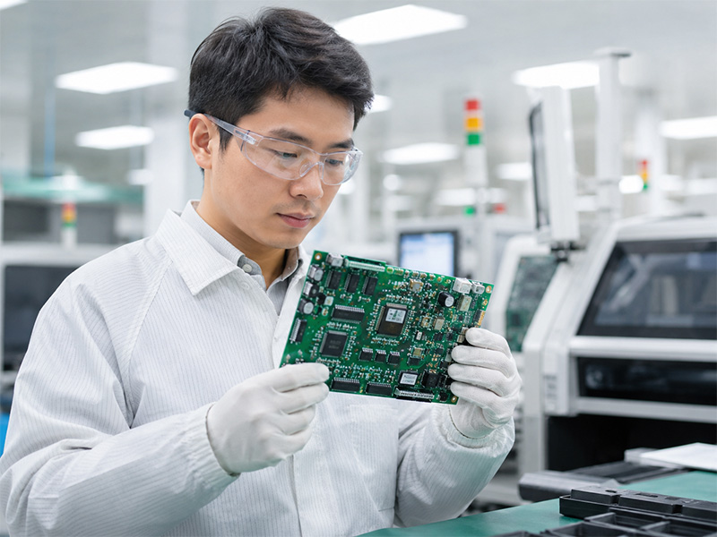
PCBA stands for printed circuit board assembly. PCBA manufacturing is the process of mounting electronic components onto a fabricated PCB and completing the soldering, inspection, and testing needed to make the assembly work.
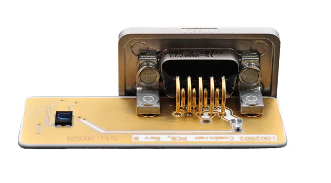
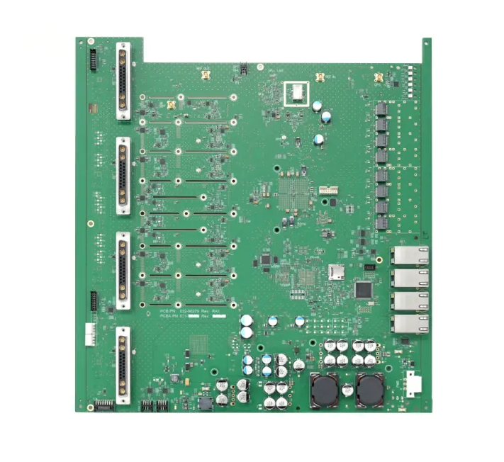
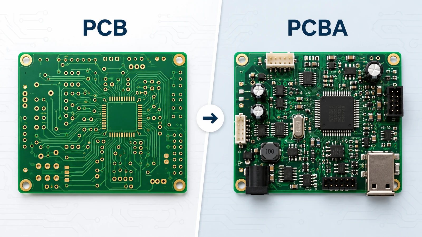
A bare PCB contains copper traces, pads, plated holes, solder mask, and surface finish. It provides the electrical interconnection but does not perform the intended product function. Once resistors, capacitors, ICs, connectors, relays, sensors, and other parts are installed, the board becomes a PCBA.
Depending on the project scope, PCBA manufacturing may include:
- Bare PCB fabrication
- Electronic component sourcing
- SMT assembly
- Through-hole assembly
- Manual soldering
- Device programming
- Electrical and functional testing
- Conformal coating or potting
- Cable installation
- Final product or box-build assembly
The term “PCB population process” is sometimes used for component placement. In most technical and purchasing contexts, however, PCB assembly process or PCBA manufacturing process is clearer.
PCBA manufacturing is also different from PCB manufacturing. PCB manufacturing produces the unassembled board. PCBA manufacturing adds the parts, solder joints, firmware, and testing required to create a usable electronic assembly.
Why Choose EBest Circuit for PCBA Manufacturing?
EBest Circuit provides PCB fabrication and PCBA assembly through one coordinated manufacturing workflow. Its PCBA manufacturing services can reduce communication gaps between the bare board supplier, component sourcing team, and assembly factory.
One-Stop PCB and PCBA Support
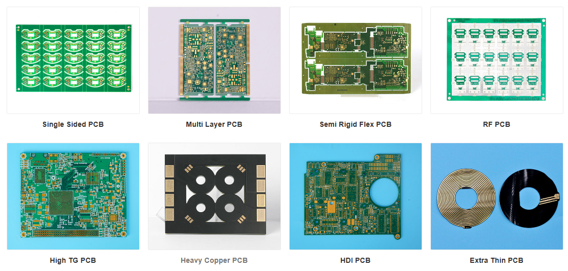
EBest Circuit supports assemblies built on several PCB types, including:
- Rigid PCB
- Flex PCB
- Rigid-flex PCB
- HDI PCB
- Aluminum PCB
- RF and microwave PCB
- Heavy copper PCB
Keeping PCB fabrication and assembly under one supplier is useful when board construction directly affects soldering. Surface finish, board warpage, pad geometry, copper distribution, panelization, and solder mask registration can all influence assembly yield.
Prototype and Production Support
Early-stage builds usually require more engineering communication than stable repeat orders. Footprint mismatches, missing polarity marks, unavailable components, and incomplete test instructions are common during prototype development.
EBest Circuit supports:
- Engineering prototypes
- Small-batch PCBA
- New product introduction
- First article builds
- Pilot production
- Repeat manufacturing
- Volume production
Many PCB prototype projects do not require a rigid minimum order quantity. The practical minimum depends on PCB panelization, stencil cost, machine setup, component packaging, and testing requirements.
Assembly and Inspection Capabilities
Available PCBA manufacturing processes include SMT, through-hole, and mixed-technology assembly. Relevant capabilities include:
- SMT placement accuracy up to ±25 μm
- 10-zone nitrogen reflow
- Solder paste inspection
- Automated optical inspection
- X-ray inspection
- Wave soldering
- Selective soldering
- In-circuit testing
- Functional testing
- MES-based production traceability
These processes support boards that combine fine-pitch ICs, BGAs, QFNs, connectors, relays, transformers, terminal blocks, and other mixed component types.
Quality Systems
EBest Circuit operates quality systems associated with industrial, medical, automotive, and aerospace electronics, including ISO9001, ISO13485, IATF16949, and AS9100D.
Certification should not replace a clear project specification. Customers should still define the required workmanship class, inspection criteria, traceability level, testing method, and documentation package.
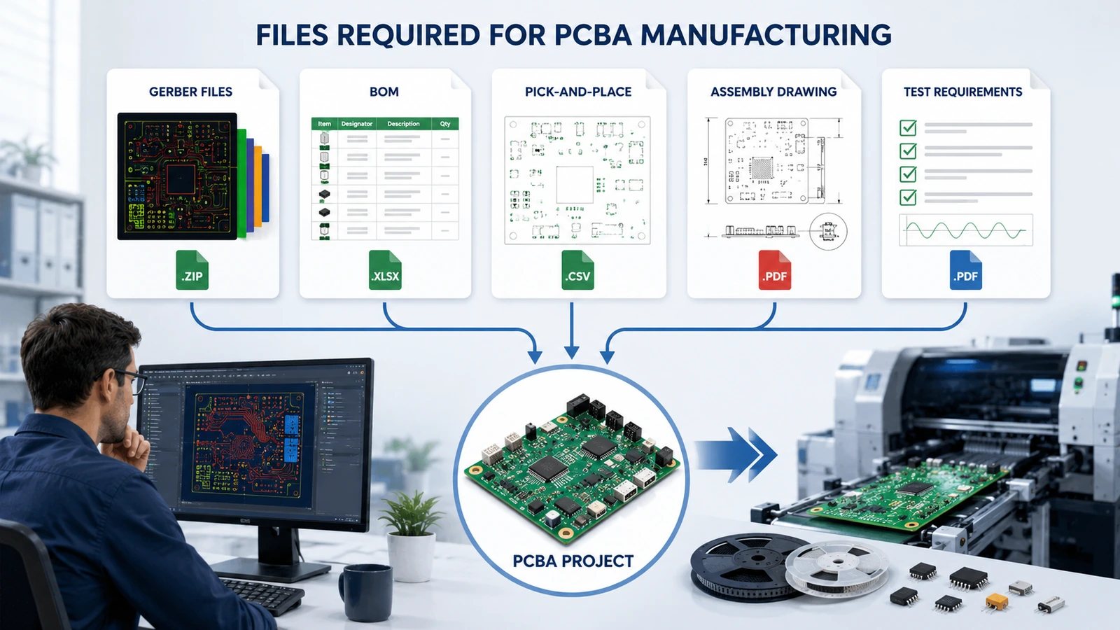
For a quotation, customers can send Gerber files, a BOM, pick-and-place data, assembly drawings, quantity, and test requirements to sales@bestpcbs.com.
PCB Manufacturing vs PCBA Manufacturing: What Is the Difference?
PCB manufacturing creates the physical circuit board. PCBA manufacturing installs the electronic components and verifies that the completed assembly meets the required electrical and functional criteria.
| Comparison Item | PCB Manufacturing | PCBA Manufacturing |
|---|---|---|
| Final output | Bare printed circuit board | Assembled electronic circuit board |
| Main inputs | Gerber or ODB++, drill files, stack-up, fabrication drawing | Bare PCB, BOM, pick-and-place file, assembly drawing |
| Main materials | Laminate, copper foil, solder mask, surface finish | Components, solder paste, flux, solder wire |
| Core processes | Imaging, etching, lamination, drilling, plating, routing | Printing, placement, reflow, insertion, soldering |
| Main equipment | Imaging systems, drills, presses, plating lines | Stencil printer, pick-and-place machine, reflow oven |
| Typical inspection | PCB AOI, electrical test, dimensional inspection | SPI, AOI, X-ray, ICT, FCT |
| Main cost drivers | Layer count, material, copper weight, dimensions, hole structure | BOM value, setup, component density, soldering, testing |
A combined PCB and PCBA supplier can simplify defect analysis when the root cause may involve pad design, board warpage, solder mask, surface finish, stencil design, or reflow conditions.
Separate sourcing can still make sense when the buyer has an approved component contract, an internal assembly line, or an established specialist supplier. The correct choice depends on responsibility, traceability, pricing transparency, and technical control rather than convenience alone.
What Files Are Required for PCBA Manufacturing?
A complete file package allows the assembler to quote accurately, prepare machine programs, check component availability, and identify manufacturing risks before production.
| File or Information | Main Purpose | Typical Problem |
|---|---|---|
| Gerber or ODB++ | Defines PCB layers, pads, mask, and board outline | Missing data or incorrect revision |
| Bill of Materials | Identifies components and sourcing requirements | Incomplete part numbers or unclear specifications |
| Pick-and-place file | Provides component coordinates and rotation | Incorrect origin, rotation, or reference designator |
| Assembly drawing | Shows locations, polarity, and special assembly notes | Missing orientation or side identification |
| Fabrication drawing | Defines dimensions, stack-up, holes, and tolerances | Conflicts with Gerber data |
| Approved vendor list | Defines acceptable manufacturers or sources | No rule for alternative components |
| Programming file | Provides firmware or configuration data | Wrong firmware revision |
| Test procedure | Defines test steps and pass/fail limits | Incomplete measurement criteria |
| Golden sample | Provides a known-good functional reference | Sample does not match current revision |
| Order requirements | Defines quantity, delivery, packaging, and compliance | Unclear scope or deadline |
The BOM should include complete manufacturer part numbers. A description such as “10 kΩ resistor” does not define package size, power rating, tolerance, voltage rating, temperature coefficient, or approved brand.
Component packaging also affects cost and manufacturability. Reels, trays, and tubes can feed automated equipment directly. Loose components or short cut strips may require manual preparation, repackaging, or placement.
All production documents should carry the same revision. A correct BOM combined with an outdated placement file can still produce incorrect assemblies.
PCBA Manufacturing Process Flow: From DFM Review to Finished Assembly
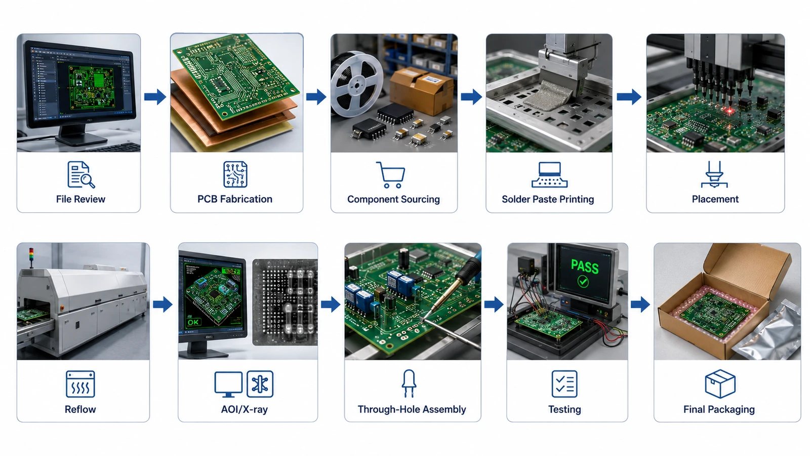
The exact process varies by product, but most PCBA projects follow the same general manufacturing flow.
File Review and DFM Analysis
The manufacturer first checks the Gerber data, BOM, placement file, assembly drawing, and testing requirements.
The review should identify:
- Component-to-footprint mismatches
- Missing polarity information
- Insufficient component clearance
- Poor fiducial design
- Unsuitable panelization
- Inaccessible test points
- Stencil aperture risks
- Conflicting document revisions
- Obsolete or long-lead components
DFM focuses on whether the PCB can be fabricated reliably. DFA addresses assembly risks. DFT checks whether the finished board can be tested efficiently.
PCB Fabrication
The bare PCB is produced according to the approved data. Surface finish, solder mask registration, pad dimensions, warpage, cleanliness, and copper balance can affect downstream soldering.
For example, excessive board warpage may reduce solder contact beneath large BGAs or bottom-terminated components. Poor solder mask definition can increase the risk of bridging on fine-pitch packages.
Component Sourcing
Components are purchased through approved manufacturers, authorized distributors, customer-nominated sources, or controlled inventory.
The sourcing review should confirm:
- Manufacturer part number
- Package type
- Lifecycle status
- Date-code requirement
- Moisture sensitivity level
- Minimum purchase quantity
- Lead time
- Approved alternatives
- Lot traceability
One unavailable semiconductor can determine the project schedule even when PCB fabrication and assembly capacity are available.
Incoming Inspection
PCBs and components are checked before production. Inspection may include:
- Part number and quantity verification
- Packaging condition
- Moisture sensitivity review
- Component marking
- PCB dimensions
- Surface finish
- Board warpage
- Certificate and lot verification
Moisture-sensitive devices may require dry storage or baking before reflow.
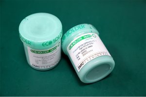
Solder Paste Printing
A stencil deposits solder paste onto the SMT pads. Stencil thickness, aperture design, printing pressure, board support, paste condition, and separation speed affect the deposited volume.
Printing quality is especially important for 01005 components, fine-pitch leads, QFNs, and BGAs. Small changes in paste volume can create opens, bridging, or excessive voiding.
Solder Paste Inspection
SPI measures paste position, area, height, and volume before component placement.
It can identify:
- Insufficient paste
- Excess paste
- Printing offset
- Bridged deposits
- Blocked apertures
- Uneven transfer
Finding a paste problem before placement prevents defective boards from continuing through reflow.
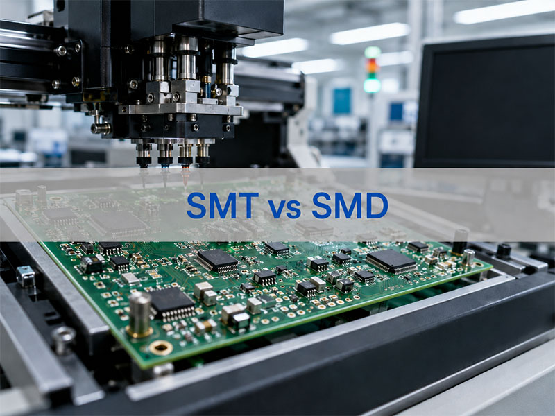
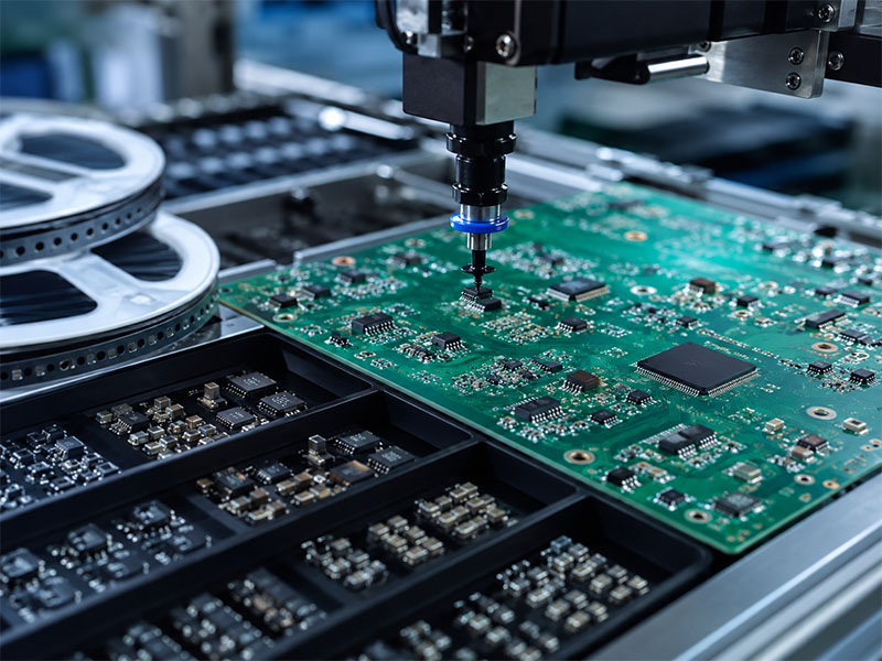
Component Placement
Pick-and-place machines position components according to the centroid data.
Setup controls normally include:
- Feeder verification
- Package confirmation
- Nozzle selection
- Vision alignment
- Polarity checking
- Fiducial recognition
- Program review
A first article board is often inspected before the full batch runs. This confirms component identity, position, rotation, and polarity.
Reflow Soldering
The populated board passes through a controlled heating profile with preheat, soak, reflow, and cooling stages.
The profile must account for:
- Solder alloy
- PCB material
- Board thickness
- Copper distribution
- Component temperature limits
- Surface finish
- Thermal mass
Nitrogen reflow can reduce oxidation and improve wetting, but it is not required for every assembly. Its value depends on package geometry, alloy, finish, and the available process window.
AOI and X-Ray Inspection
AOI inspects visible component and soldering features, including:
- Missing components
- Placement shift
- Incorrect polarity
- Wrong component marking
- Visible solder bridges
- Exposed solder joint quality
X-ray is used for hidden connections such as:
- BGA solder balls
- QFN thermal pads
- Bottom-terminated components
- Hidden connector joints
- Via-in-pad structures
Neither method confirms full electrical function. They should be combined with electrical or functional testing where product risk justifies it.
Through-Hole Assembly
Through-hole components may be inserted manually or automatically, then soldered by wave, selective, or controlled hand soldering.
The process choice depends on:
- Number of through-hole joints
- Bottom-side SMT components
- Connector geometry
- Component heat sensitivity
- Board thermal mass
- Production volume
- Required barrel fill
Selective soldering is often suitable when only a few through-hole components are present or when nearby SMT parts cannot tolerate wave soldering.
Cleaning and Secondary Operations
Cleaning may be required by the flux chemistry, coating process, voltage level, leakage-current limits, or customer specification.
Secondary operations can include:
- Device programming
- Depanelization
- Heat sink installation
- Cable assembly
- Conformal coating
- Potting
- Mechanical assembly
- Serial-number labeling
“No-clean” flux does not mean the residue is acceptable for every application. High-voltage, high-impedance, medical, optical, and coated assemblies may require stricter cleanliness controls.
Electrical and Functional Testing
Testing may include continuity checks, flying probe testing, ICT, boundary scan, firmware verification, and functional testing.
A practical PCB testing plan should address the most likely failure modes. Adding every available test increases cost without necessarily improving useful coverage.
Final Inspection and Packaging
Before shipment, the manufacturer verifies:
- Visual condition
- Labels and serial numbers
- Firmware revision
- Test records
- Quantity
- Packaging
- Customer-specific documentation
Electrostatic-sensitive, moisture-sensitive, or mechanically fragile assemblies require suitable protective packaging.
SMT, Through-Hole, and Mixed-Technology PCBA Manufacturing
The assembly method should match the component types, board density, mechanical loading, and expected production volume.
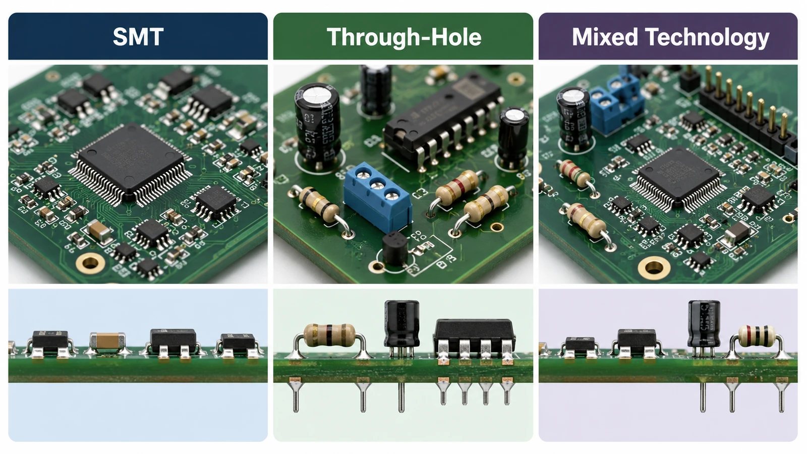
| Factor | SMT Assembly | Through-Hole Assembly | Mixed-Technology Assembly |
|---|---|---|---|
| Mounting method | Components soldered to surface pads | Leads inserted through plated holes | Combines both methods |
| Assembly density | High | Lower | Medium to high |
| Automation | High | Moderate | Depends on product |
| Typical components | ICs, resistors, capacitors, semiconductors | Connectors, relays, transformers, large capacitors | Industrial, power, control, and communication boards |
| Mechanical retention | Suitable for most low-load parts | Strong lead-to-hole retention | Selected by component requirement |
| Soldering method | Reflow | Wave, selective, or hand soldering | Reflow plus secondary soldering |
| Main limitation | Some high-force parts need additional support | Uses more board area and labor | Requires more process stages |
SMT suits compact products, dense layouts, and automated production. Components can be installed on both sides of the PCB, and the shorter interconnections also benefit many high-speed circuits.
Through-hole assembly remains useful for connectors, switches, relays, transformers, and parts exposed to repeated insertion force. It should not be used automatically for every large component. A correctly designed SMT joint may be sufficient when mechanical loading is limited.
Mixed assembly is common in industrial controls, power electronics, medical devices, automotive modules, and communication equipment. A typical sequence completes SMT reflow first, followed by through-hole insertion and selective soldering.
How Is Quality Controlled During PCBA Manufacturing?
Quality control combines incoming inspection, process monitoring, visual inspection, hidden-joint inspection, electrical testing, and traceability.
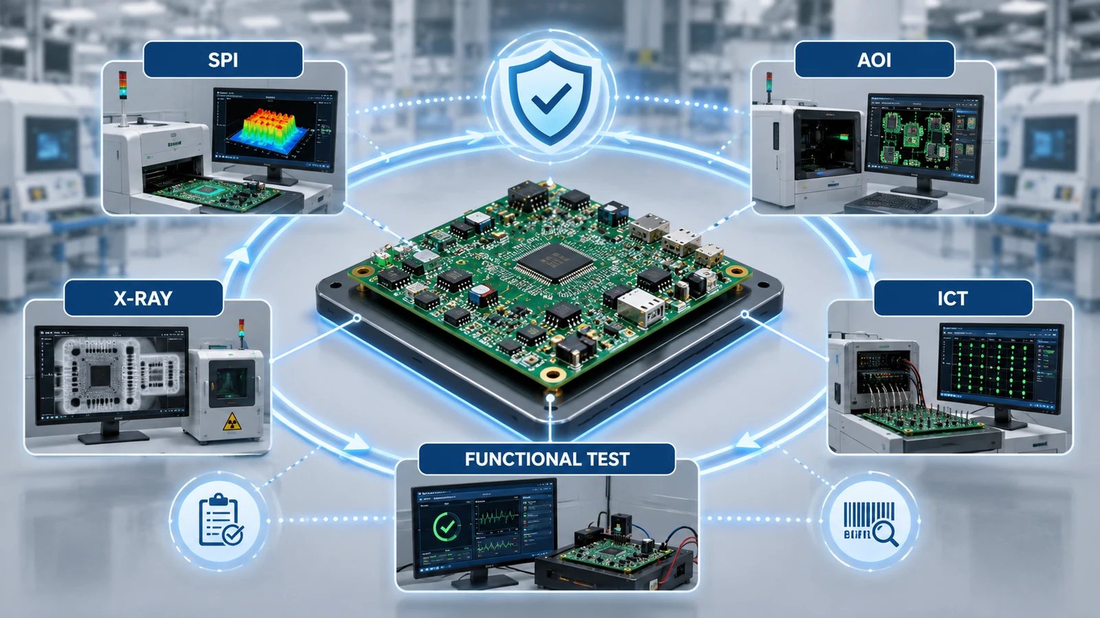
| Method | Main Purpose | Typical Findings | Limitation |
|---|---|---|---|
| Incoming inspection | Verify PCBs and components | Wrong parts, damage, packaging issues | Does not confirm assembled performance |
| SPI | Measure solder paste | Low volume, excess paste, offset | Used before reflow |
| First article inspection | Confirm initial setup | Wrong value, position, or polarity | Covers the initial build only |
| AOI | Inspect visible features | Missing parts, shift, polarity, solder defects | Cannot fully inspect hidden joints |
| X-ray | Inspect hidden solder joints | BGA opens, bridges, voiding | Does not prove function |
| Flying probe | Test low-volume assemblies | Opens, shorts, selected component faults | Slower than dedicated ICT |
| ICT | Test networks and component values | Opens, shorts, wrong values | Requires test access and often a fixture |
| FCT | Verify product operation | Interface, firmware, signal, and power faults | Coverage depends on the test procedure |
| Burn-in | Screen selected early failures | Temperature- or time-related faults | Adds cost and production time |
Process Control
Stable production depends on more than final inspection. Important controls include:
- Solder paste storage and handling
- Stencil condition
- Printer setup verification
- Feeder loading control
- Reflow profile management
- Moisture-sensitive component handling
- Equipment calibration
- First article approval
- Controlled repair procedures
Traceability
The required traceability level should reflect product risk.
A basic prototype may need only a batch number and final test result. Automotive, medical, aerospace, and other high-reliability products may require records linking the finished PCBA to:
- PCB production lot
- Component lot or date code
- Solder paste batch
- Machine program
- Inspection result
- Test data
- Repair history
- Firmware revision
EBest Circuit uses MES-based records to support production and material traceability. Customers should define the required record retention, component-level tracking, and reporting format before production.
Acceptance Standards
IPC-A-610 is commonly used for electronic assembly acceptance, while J-STD-001 addresses soldered electrical and electronic assembly requirements.
The purchase specification should state the required class, revision, exceptions, and documentation. A general note such as “manufacture to IPC” is too broad for controlled production.
Common PCBA Manufacturing Defects and Their Causes
Many assembly defects have more than one possible cause. The process team should identify the origin rather than only repairing the visible symptom.
| Defect | Likely Causes | Detection | Prevention |
|---|---|---|---|
| Solder bridge | Excess paste, misalignment, poor pad spacing | AOI, X-ray, electrical test | Optimize stencil, printing, and layout |
| Insufficient solder | Blocked aperture, poor transfer, weak wetting | SPI, AOI, X-ray | Maintain stencil and control paste release |
| Tombstoning | Uneven heating, unequal pad geometry, placement offset | AOI | Balance pads and thermal connections |
| Component shift | Placement error, paste movement, unstable reflow | AOI | Improve placement and profile control |
| Missing component | Feeder or pickup failure | AOI, first article inspection | Verify feeders and setup |
| Wrong component | BOM error, reel mix-up, weak material control | AOI, ICT, manual check | Use barcode and approved BOM control |
| Reversed polarity | Incorrect drawing or rotation data | AOI, FCT | Provide clear polarity and centroid data |
| Cold joint | Insufficient heat, contamination, oxidation | AOI, electrical test | Control profile, storage, and cleanliness |
| BGA open | Warpage, low paste, poor collapse | X-ray, ICT, FCT | Control coplanarity, paste, and profile |
| Excessive voiding | Pad design, volatiles, thermal profile | X-ray | Adjust stencil pattern, paste, and reflow |
| Solder balling | Excess paste, moisture, poor preheat | AOI | Control paste volume and component condition |
| Lifted pad | Excessive rework heat or mechanical force | Visual inspection | Limit rework cycles and use controlled tools |
Some problems originate in the PCB design rather than the production line. Incorrect footprints, missing solder mask dams, uneven thermal connections, poor fiducial placement, and inaccessible test points may require a design revision.
What Determines PCBA Manufacturing Cost and Lead Time?
A PCBA quotation normally includes the bare board, components, assembly, tooling, testing, and any secondary operations.
| Cost or Schedule Factor | Cost Effect | Lead-Time Effect |
|---|---|---|
| PCB complexity | Special materials and structures raise fabrication cost | More manufacturing stages are required |
| BOM value | Semiconductors and connectors may dominate total cost | Long-lead parts can delay production |
| Order quantity | Setup cost is spread across more units | Larger orders require more line capacity |
| Component packaging | Reels and trays support automation | Loose parts need additional preparation |
| Fine-pitch or BGA parts | Tighter control and X-ray may be required | Inspection adds processing time |
| Through-hole content | More insertion and soldering labor | Manual work reduces throughput |
| Double-sided SMT | Requires another print, placement, and reflow cycle | Adds an assembly stage |
| ICT fixture | Adds tooling cost | Fixture development requires time |
| Functional testing | Depends on equipment and cycle time | Long tests can limit daily output |
| Programming | Adds handling and verification | Firmware must be ready before release |
| Coating or potting | Adds material, masking, curing, and inspection | Curing extends the schedule |
| Box build | Adds mechanical parts and labor | Requires more materials and workstations |
Component availability frequently has the greatest influence on total lead time. Assembly may require only a few days after all materials arrive, while one unavailable IC can delay the complete project.
A quotation request should include:
- Complete manufacturer part numbers
- Rules for alternative components
- Prototype and production quantities
- Expected repeat demand
- Test requirements
- Programming files
- Coating or potting requirements
- Packaging instructions
- Target delivery date
EBest Circuit can quote PCB fabrication, component sourcing, assembly, inspection, and testing as one package. Standard production may take approximately 3–5 days for suitable projects after materials and approved engineering data are available.
Complex PCB structures, unavailable components, custom fixtures, conformal coating, potting, or box build require additional time. An expedited assembly schedule should therefore be confirmed against actual material status rather than assembly capacity alone.
Prototype, Low-Volume, and Mass-Production PCBA Manufacturing
The manufacturing objective changes as the project moves from prototype to volume production.
| Stage | Main Objective | Recommended Controls | Common Mistake |
|---|---|---|---|
| Prototype | Verify design and function | DFM review, flexible sourcing, first article inspection | Expecting volume pricing |
| Low-volume build | Stabilize the process | Yield review, BOM confirmation, test refinement | Ignoring setup and test cost |
| Pilot run | Confirm production readiness | Fixture validation, work instructions, traceability | Scaling before defects are closed |
| Mass production | Maintain consistency and cost | SPC, sourcing control, capacity planning | Changing parts without approval |
| Repeat order | Reproduce an approved build | Revision control and retained programs | Assuming stock and pricing remain unchanged |
Prototype Builds
A prototype should identify:
- Footprint errors
- Mechanical interference
- Incorrect polarity
- Power or signal problems
- Firmware issues
- Test-access limitations
- Assembly risks
- Component availability problems
A prototype that powers on is not automatically ready for volume production. The design must also be repeatable, testable, and supportable by the supply chain.
Low-Volume and Pilot Production
Low-volume builds help confirm whether the assembly process is stable. This stage is suitable for refining the reflow profile, validating the test procedure, checking yield, and approving alternative components.
Pilot production should use processes close to the intended mass-production method. Excessive manual adjustment can hide problems that will return at higher volume.
Mass Production
Volume manufacturing requires:
- Released and controlled files
- Approved sourcing channels
- Defined alternative-part rules
- Stable machine programs
- Documented inspection criteria
- Validated test fixtures
- Repair and deviation procedures
- Batch traceability
- Capacity planning
EBest Circuit supports projects from engineering prototypes through repeat production. Keeping PCB data, component sourcing, assembly records, and engineering changes within one workflow can simplify scaling.
How to Choose a PCBA Contract Manufacturer?
A suitable contract manufacturer should match the product’s technical risk, volume, industry requirements, and expected lifecycle.
Confirm the Scope
Check whether the supplier provides:
- PCB fabrication
- Component sourcing
- SMT assembly
- Through-hole assembly
- Programming
- Electrical testing
- Functional testing
- Coating or potting
- Box build
- Failure analysis
Some manufacturers outsource part of the work. That is not automatically a problem, but ownership of quality, traceability, and corrective action should be clear.
Match the Equipment to the Product
Confirm that the factory can process the actual component and PCB features in the design, such as:
- Fine-pitch ICs
- BGAs
- QFNs and LGAs
- 01005 components
- Double-sided SMT
- Large bottom-terminated packages
- Heavy connectors
- Press-fit components
- Flex or rigid-flex assemblies
- High-current terminals
A general statement such as “we support SMT” does not confirm suitability for every package or board structure.
Review Test Coverage
The inspection and test plan should match the product risk.
Examples include:
- SPI for fine-pitch paste printing
- X-ray for BGA and QFN joints
- ICT for assemblies with suitable test access
- Flying probe for prototypes or low-volume orders
- FCT for firmware-controlled or interface-dependent products
Ask what the supplier means by “100% tested.” In some quotations, this may refer only to visual inspection or a simple power-on check.
Examine Component-Sourcing Controls
The manufacturer should explain:
- Approved sourcing channels
- Counterfeit-risk controls
- Alternative-part approval
- Date-code requirements
- Moisture-sensitive storage
- Customer-supplied material handling
- Excess-component ownership
- Lot traceability
A low assembly price may be offset by unclear component sources, unnecessary minimum purchases, or weak handling of unused stock.
Evaluate Engineering Communication
Useful indicators include:
- Specific DFM comments
- Clear BOM questions
- Controlled file revisions
- Written substitution approval
- Traceable engineering changes
- Defined deviation procedures
- Named technical contacts
Fast communication is useful, but accurate engineering communication prevents more expensive production errors.
Compare Quotations on the Same Scope
A clear quotation should separate:
- PCB cost
- Component cost
- Assembly cost
- Stencil and tooling
- Programming
- Testing
- Coating or potting
- Box-build work
- Freight
- Excess material
Two quotations are not directly comparable when one includes functional testing and the other includes only visual inspection.
FAQ
1. What does PCBA manufacturing mean?
PCBA manufacturing is the process of mounting electronic components onto a bare PCB and completing the soldering, inspection, programming, and testing required to create a functional assembly.
2. What is the difference between PCB and PCBA manufacturing?
PCB manufacturing produces the unassembled circuit board. PCBA manufacturing installs and solders the components and may also include programming, testing, coating, and final assembly.
3. What are the main steps in the PCBA manufacturing process?
The process usually includes file review, PCB fabrication, component sourcing, incoming inspection, solder paste printing, SPI, placement, reflow, AOI or X-ray, through-hole assembly, testing, final inspection, and packaging.
4. What files are required for PCBA manufacturing?
Most projects need Gerber or ODB++ data, a BOM, pick-and-place file, assembly drawing, order quantity, and test requirements. Programming files and a golden sample may also be required.
5. What is SMT in PCBA manufacturing?
SMT, or surface-mount technology, places components directly onto pads on the PCB surface. It supports compact layouts, high component density, and automated production.
6. What is the difference between SMT and through-hole assembly?
SMT components are soldered to surface pads. Through-hole leads pass through plated holes before soldering. Through-hole assembly is commonly used for connectors, relays, transformers, and mechanically loaded parts.
7. How long does PCBA manufacturing take?
Assembly may take several days after all PCBs, components, files, and test instructions are ready. The total lead time depends mainly on component availability, PCB complexity, quantity, testing, and secondary processes.
8. What determines PCBA manufacturing cost?
The main factors are PCB complexity, BOM value, quantity, setup, component packaging, fine-pitch parts, through-hole labor, inspection, programming, testing, tooling, coating, and box build.
9. What is the difference between SPI, AOI, X-ray, ICT, and FCT?
SPI checks solder paste. AOI checks visible components and solder joints. X-ray examines hidden joints. ICT tests electrical networks and component values. FCT verifies actual product operation.
10. Can one supplier handle both PCB manufacturing and PCBA assembly?
Yes. A one-stop supplier can fabricate the board, source components, assemble the PCBA, test it, and complete secondary processes. The supplier’s actual capabilities and responsibility boundaries should still be verified.
11. Does EBest Circuit support prototypes and small-batch PCBA?
Yes. EBest Circuit supports engineering prototypes, small-batch production, pilot runs, repeat orders, and volume manufacturing.
12. What PCBA testing services does EBest Circuit provide?
Available services include SPI, AOI, X-ray, ICT, functional testing, and customer-defined test procedures. The suitable combination depends on package type, test access, quantity, and product risk.
13. Can EBest Circuit source electronic components?
Yes. EBest Circuit can source components as part of turnkey or partial-turnkey PCBA manufacturing. Customers should provide complete part numbers and state whether alternatives are permitted.
14. What certifications does EBest Circuit have?
EBest Circuit operates quality systems that include ISO9001, ISO13485, IATF16949, and AS9100D. Customers should still define the exact acceptance, documentation, and traceability requirements for the project.
15. How can I request a PCBA manufacturing quotation?
Send the Gerber files, BOM, pick-and-place data, assembly drawings, quantity, test requirements, and target delivery date to sales@bestpcbs.com. Include firmware, coating, packaging, and box-build requirements where applicable.