PCB manufacturing PCB manufacturing
Home > Blog

potting vs conformal coating

Conformal Coating vs Potting: Which PCB Protection Is Right for You?
Wednesday, April 15th, 2026

When it comes to protecting your PCB from environmental hazards, mechanical stress and premature failure you’re likely weighing conformal coating vs potting but which one delivers the right balance of protection, cost and practicality for your project? As an electronics engineer with over a decade of experience designing and testing PCB protection solutions I’ve seen firsthand how the wrong choice leads to costly field failures, missed deadlines and frustrated clients.

In this guide I’ll break down conformal coating vs potting in simple straightforward terms, comparing their processes, materials, protection levels, repairability and cost so you can make an informed decision that aligns with your project’s unique needs. We’ll cover everything from application steps to real-world use cases and common mistakes to avoid, ensuring you get the most value from your PCB protection investment.

Conformal Coating vs Potting, https://www.bestpcbs.com/blog/2026/04/conformal-coating-vs-potting/

What Are Conformal Coating and Potting and Why Do PCBs Need Them?

PCBs are the backbone of nearly every electronic device from consumer gadgets to industrial machinery but they are delicate and susceptible to damage from moisture, dust, chemicals, vibration and temperature extremes. Without proper protection these threats cause corrosion, short circuits, solder joint failures and component damage, leading to reduced product lifespan, increased warranty claims and safety hazards.

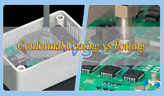
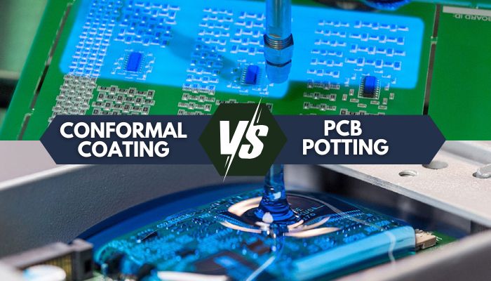
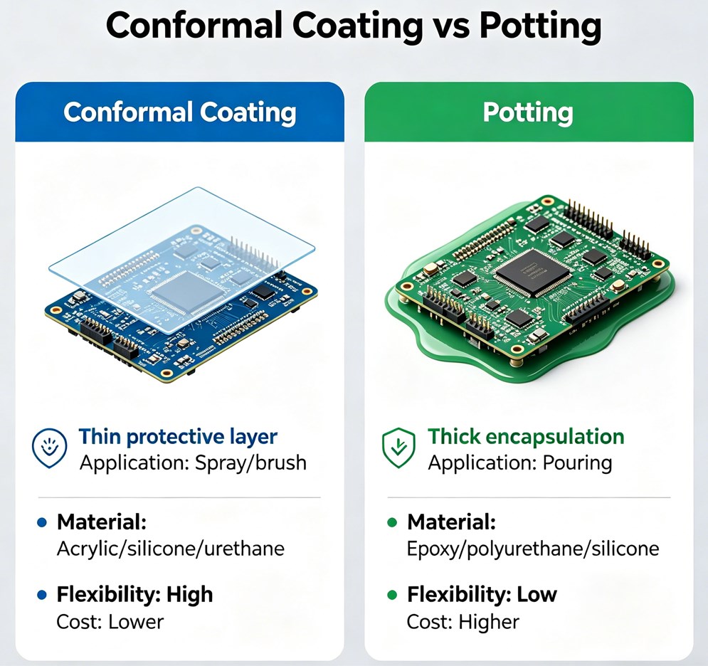
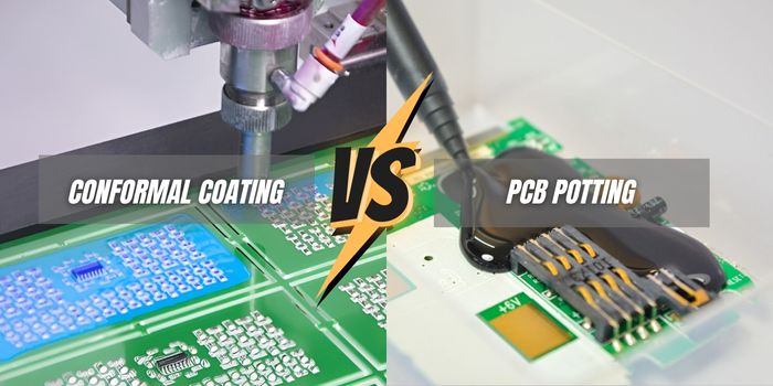
Conformal coating and potting are the two most common PCB protection methods each designed to shield boards but with distinct approaches. Conformal coating is a thin protective film applied directly to the PCB surface, conforming to component shapes to create a barrier against contaminants.

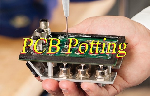
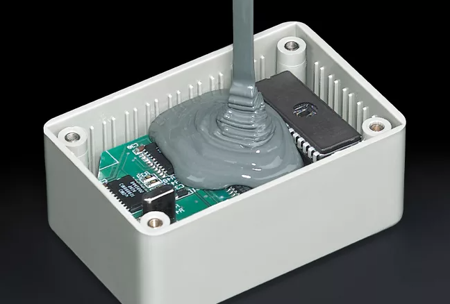
Potting involves completely encapsulating the PCB in a thick solid resin, forming an impenetrable shield against harsh conditions. Both methods are critical for ensuring PCB reliability, but choosing the right one depends on your application’s environment, size, weight and budget constraints.

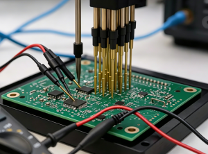
How Do Conformal Coating and Potting Differ in Application Process?

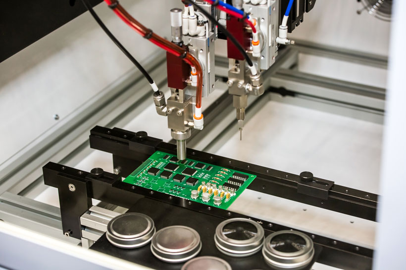
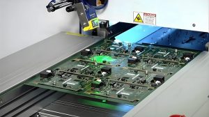
The application processes for conformal coating and potting are fundamentally different, with distinct steps, equipment and preparation requirements. Conformal coating is a simpler, faster process ideal for high-volume production, while potting is more labor-intensive and suited for applications requiring maximum protection.

Below is a detailed comparison of their application processes to help you understand what each entails.

Process StepConformal CoatingPotting
Prep WorkClean the PCB with isopropyl alcohol to remove flux residue dust and oils. Mask areas that should not be coated such as connectors test points and gold fingers using tape or liquid masking agents.Thoroughly clean and dry the PCB to remove all contaminants. Place the PCB in a mold or housing that fits its size and shape ensuring all components are properly positioned.
Application MethodCommon methods include spraying dipping brushing or selective automated coating. Spraying is ideal for large volumes while brushing works for small batches or touch-ups.Mix two-part resin (epoxy polyurethane or silicone) per manufacturer instructions. Pour or inject the resin into the mold covering the PCB completely without air bubbles.
CuringCures at room temperature (24-48 hours) or with heat (60-80°C for 30-60 minutes) depending on the material. UV-curable coatings cure in seconds with UV light for faster production.Requires longer curing time (24-72 hours at room temperature) or heat curing (80-100°C for 1-2 hours). The mold must remain undisturbed during curing to avoid defects.
Post-ApplicationRemove masking materials. Inspect for coverage gaps bubbles or uneven coating using a magnifying glass or microscope. Touch up any missed areas as needed.Remove the PCB from the mold once fully cured. Trim excess resin and inspect for voids cracks or incomplete encapsulation. No touch-ups are possible without damaging the potting.

Which Offers Better Environmental Protection: Conformal Coating vs Potting?

Environmental protection is the primary goal of both conformal coating and potting, but their effectiveness varies significantly based on the threat level. Potting provides superior environmental protection as it completely encapsulates the PCB, creating an impenetrable barrier against moisture, dust, chemicals and extreme temperatures.

Conformal coating offers good protection for moderate environments but cannot match potting’s resistance to harsh conditions. The table below breaks down their performance against common environmental threats to help you determine which is right for your application.

Environmental ThreatConformal CoatingPottingWinner
Moisture/HumidityBlocks light moisture and humidity but may fail if the coating is cracked or uneven. Not suitable for submersion or high-humidity industrial environments.Completely seals the PCB preventing any moisture ingress even in submersion (IP67/IP68 ratings) or high-humidity conditions.Potting
Dust/ParticulatesCovers the PCB surface blocking dust and debris but may not seal gaps between components where particles can accumulate.Encases the entire PCB leaving no gaps for dust or particulates to enter providing complete protection.Potting
Chemicals/SolventsResistant to mild chemicals but may degrade when exposed to harsh solvents (e.g. industrial cleaners oils).Highly resistant to harsh chemicals solvents and oils depending on the resin type (epoxy offers the best chemical resistance).Potting
Temperature ExtremesPerforms well in moderate temperatures (40°C to 125°C) with silicone coatings offering wider ranges (60°C to 200°C).Handles extreme temperatures (50°C to 200°C) with silicone potting compounds providing the best thermal stability for high-heat applications.Potting

Why Is Repairability a Key Consideration Between Conformal Coating and Potting?

Repairability is a critical factor when choosing between conformal coating and potting because it directly impactsmaintenance costs and project timelines. Conformal coating is easily repairable, making it ideal for projects where PCBs may need troubleshooting or component replacement.

Potting is nearly impossible to repair without destroying the PCB, as the solid resin cannot be removed without damaging components. For example, if a component fails on a conformal coated PCB, you can simply strip the coating from the affected area, repair or replace the component, and reapply the coating.

On a potted PCB, you would need to break open the resin, which often damages surrounding components, rendering the entire board useless. This makesrepairability a non-negotiable consideration for projects with long lifespans or high maintenance requirements, such as consumer electronics or medical devices.

Conformal Coating vs Potting, https://www.bestpcbs.com/blog/2026/04/conformal-coating-vs-potting/

How Do Conformal Coating and Potting Impact PCB Weight and Size?

PCB weight and size are critical for compact applications such as wearables, consumer electronics and aerospace devices, andconformal coating and potting have vastly different impacts on both. Conformal coating adds minimal weight and size as it is a thin layer (25-250 microns) that conforms to the PCB’s shape.

It adds less than 5% to the PCB’s total weight and no noticeable bulk, making it ideal for small, lightweight designs. Potting adds significant weight and size because it requires a thick resin layer (1-15mm+) and often a mold or housing to contain the resin.

It can increase the PCB’s weight by 50-200% and double its size depending on the resin thickness and mold design. The table below summarizes their impact on weight and size for quick reference.

FactorConformal CoatingPotting
Layer Thickness25-250 microns (thin film)1-15mm+ (thick solid resin)
Weight ImpactAdds <5% of PCB weightAdds 50-200% of PCB weight
Size ImpactNo noticeable bulk; maintains PCB’s original footprintIncreases size by 50-100%; requires additional space for mold/housing
Ideal ForCompact lightweight designs (wearables consumer electronics)Applications where size/weight are not critical (industrial machinery outdoor sensors)

Which Is More Cost-Effective for My Project: Conformal Coating vs Potting?

Cost-effectiveness depends on your project’s volume, protection needs and long-term maintenance. Conformal coating is more cost-effective for most projects, especially high-volume production, with lower material, labor and maintenance costs due to its thin layers, fast application and easy repairability.

Potting is more expensive upfront (higher resin, labor and mold costs) and long-term (failed PCBs must be replaced). Potting is worth the cost for small-batch or maximum-protection projects; conformal coating is better forhigh-volume or cost-sensitive ones.

The table below breaks down cost factors between conformal coating vs potting.

Cost FactorConformal CoatingPotting
Material CostLow; thin layers require minimal materialHigh; thick resin layers and mold materials add cost
Labor CostLow; fast application (automated options available for high volume)High; labor-intensive mixing pouring and curing steps
Maintenance CostLow; easy repairability reduces replacement costsHigh; failed PCBs must be replaced entirely
Total Cost (High Volume)Significantly lower (30-50% less than potting)Higher due to material and labor expenses

What Materials Are Used for Conformal Coating vs Potting and How Do They Compare?

Both conformal coating and potting use similar resin materials but they are formulated differently to suit their respective applications. Thekey materials for each method and their performance characteristics are critical to choosing the right protection.

Below is a detailed comparison of the most common materials used for conformal coating vs potting.

Material TypeConformal Coating UsePotting UseKey Characteristics
AcrylicMost common; used for general-purpose protectionRare; only for low-stress applicationsLow cost easy to apply easy to repair. Poor chemical resistance; not suitable for harsh environments.
SiliconeUsed for high-temperature or flexible applicationsCommon; used for high-temperature or vibration-prone applicationsExcellent temperature range (60°C to 200°C) flexible. Good moisture resistance; lower mechanical strength.
PolyurethaneUsed for chemical or moisture-prone applicationsCommon; used for general-purpose pottingGood chemical and moisture resistance. Flexible; moderate temperature range (40°C to 125°C).
EpoxyRare; used for high-strength applicationsMost common; used for maximum protectionHigh mechanical strength excellent chemical resistance. Rigid; poor repairability; temperature range (40°C to 150°C).
Conformal Coating vs Potting, https://www.bestpcbs.com/blog/2026/04/conformal-coating-vs-potting/

When Should I Choose Conformal Coating Over Potting for My PCB?

Choose conformal coating over potting in the following scenarios, where its unique advantages align with your project needs:

  • Compact size and lightweight design: Ideal for wearables, smartwatches, portable consumer electronics, or drone flight control boards. Conformal coating adds minimal bulk and weight (less than 5% of the PCB’s total weight), maintaining the PCB’s original footprint without compromising protection for moderate environments.
  • High-volume production and cost-effectiveness: Suitable for mass-produced consumer electronics, basic household appliances, or low-cost IoT devices. Conformal coating has lower material and labor costs, with faster application times (including automated spraying options) that support large-scale manufacturing without sacrificing quality or efficiency.
  • Repairability as a priority: Perfect for medical devices (like portable heart rate monitors), telecommunications equipment, or any PCB that may need troubleshooting, component replacement, or maintenance after installation. Conformal coating can be easily stripped from specific areas, repaired, and reapplied without damaging the board or surrounding components.
  • Post-installation component access: For PCBs with test points, connectors, gold fingers, or USB ports. Conformal coating can be precisely masked in these areas to keep them accessible for testing, calibration, or connection, while still protecting the rest of the PCB from light moisture and dust.
  • Moderate environmental conditions: Suitable for indoor electronics, office equipment, or devices not exposed to harsh chemicals, submersion, or extreme vibration. Conformal coating provides adequate protection against light moisture, dust, and moderate temperature fluctuations (40°C to 125°C) for these applications.
  • Flexible or vibration-prone PCBs: Ideal for automotive electronic control units (ECUs), portable medical devices, or industrial automation sensors. Flexible conformal coatings (like silicone-based options) can withstand temperature changes and mechanical stress without cracking, ensuring long-term reliability.
  • Fast-turnaround protection: Perfect for prototype PCBs, small-batch production runs, or emergency repairs. Conformal coating cures quickly—UV-curable options cure in seconds, while standard coatings cure in 24-48 hours—allowing for faster project completion compared to potting’s 24-72 hour curing time.
  • Low- to medium-voltage PCBs: Suitable for consumer electronics, basic IoT sensors, or small power supplies. Conformal coating provides sufficient electrical insulation for these applications without the added cost and bulk of potting.
  • Strict size constraints: Ideal for aerospace components (where weight and space are critical), compact wearables, or miniaturized medical devices. Conformal coating’s thin layer (25-250 microns) ensures it does not add noticeable bulk, making it ideal for space-limited designs.
  • Post-protection visual inspection: For applications where visual inspection of the PCB is necessary, such as quality control checks or troubleshooting. Most conformal coatings are transparent or translucent, allowing you to visually inspect components, solder joints, and traces without removing the protective layer.

When Is Potting a Better Choice Than Conformal Coating for Harsh Environments?

Choose potting over conformal coating in harsh environments or scenarios where maximum protection is non-negotiable, including the following:

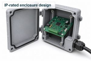
  • Submersion or high humidity: For outdoor sensors, subsea instrumentation, marine electronics, or devices used in damp industrial settings. Potting provides an impenetrable seal that meets IP67 or IP68 ratings, preventing any moisture ingress that could cause corrosion, short circuits, or component failure.
  • Harsh chemicals, solvents, or oils: Ideal for factory machinery, chemical processing equipment, or automotive under-hood components. Potting resins—especially epoxy—offer superior chemical resistance that conformal coating cannot match, protecting the PCB from degradation, swelling, or breakdown caused by exposure to harsh substances.
  • Extreme vibration or mechanical stress: Suitable for automotive engine components, heavy industrial machinery, construction equipment, or aerospace devices. The thick solid resin of potting absorbs vibration, stabilizes components, and reinforces solder joints, reducing the risk of mechanical damage and premature failure.
  • High-temperature environments: Perfect for aerospace components, industrial heaters, power electronics, or devices operating near heat sources. Silicone potting compounds handle extreme temperatures (50°C to 200°C) and provide better thermal stability than most conformal coatings, ensuring consistent performance even in prolonged high-heat conditions.
  • Tamper resistance required: For military electronics, security devices, proprietary equipment, or medical devices with sensitive circuitry. Potting encases the entire PCB in a solid resin barrier, making it difficult to access, modify, reverse engineer, or tamper with, protecting intellectual property and ensuring device integrity.
  • Heavy dust or particulate matter: Ideal for construction site sensors, mining equipment, or outdoor industrial controls. Potting completely seals the PCB, leaving no gaps for dust or particulates to enter, preventing clogging, short circuits, or component wear caused by debris accumulation.
  • High-voltage applications: Suitable for power supplies, industrial transformers, or high-voltage control systems. Potting provides superior electrical insulation and arc suppression compared to conformal coating, preventing arcing between components and reducing the risk of electrical failures or safety hazards.
  • Long-term outdoor use: Perfect for outdoor lighting controls, agricultural sensors, or remote monitoring devices. Potting’s durable resin barrier resists UV radiation, weathering, and environmental degradation, ensuring the PCB maintains reliability for 10-20 years or longer, even in unprotected outdoor settings.
Conformal Coating vs Potting, https://www.bestpcbs.com/blog/2026/04/conformal-coating-vs-potting/

FAQ: Common Questions About Conformal Coating vs Potting

Q1: Which provides better thermal management: conformal coating or potting?

A1: Potting is better, especially with thermally conductive resins. Its thick layer dissipates heat more effectively than thin conformal coating. Silicone potting is optimal for thermal management; conformal coating has limited heat dissipation, unsuitable for high-heat components.

Q2: What common mistakes should I avoid when choosing between them?

A2: Avoid choosing potting for compact/repairable applications and conformal coating for harsh environments. Don’t skip surface preparation or overlook resin-component compatibility.

Q3: Can I use both conformal coating and potting?

A3: Yes, for enhanced protection in extreme environments (e.g., coat first, then pot). It’s common in aerospace/military but adds cost, weight and complexity.

Q4: Is potting better for high-voltage PCBs?

A4: Yes. Potting offers superior electrical insulation and arc suppression, critical for high-voltage use. Conformal coating is only suitable for low to medium-voltage PCBs.

Q5: How long do they last on a PCB?

A5: Conformal coating lasts 5-10 years (acrylic 5-7 years, silicone/polyurethane 7-10 years). Potting lasts 10-20+ years. Proper prep and material selection extend lifespan.

You may also like

PCB Potting: Guide to Materials, Process, Cost & Protection Methods
Thursday, March 19th, 2026

PCB potting is one of the most reliable ways to protect printed circuit boards in demanding working conditions, and it has become a staple process for industrial, automotive, outdoor, and mission-critical electronic devices. Proper potting turns a fragile circuit board into a durable, long-lasting component that stands up to moisture, vibration, and chemical exposure. Too many teams overlook PCB protection until failures happen, but a small investment in quality potting avoids costly downtime, replacements, and customer complaints down the line.

In this complete guide, we’ll break down every detail you need to know about PCB potting. We’ll start with the core definition, move into its standout benefits, compare it to other common protection methods, walk through the full process, and answer the most frequently asked questions from engineers and procurement teams. Whether you’re researching PCB potting services for a bulk order, choosing the right PCB potting material for your project, or troubleshooting common issues like air bubbles, this guide has practical, field-tested advice you can use right away.

PCB Potting, https://www.bestpcbs.com/blog/2026/03/pcb-potting/

What is PCB Potting?

PCB potting is a way to protect a circuit board by covering it completely with a liquid material that later hardens. After the PCB is assembled, it is placed in a case. Then a potting compound, such as epoxy or silicone, is poured over it. The liquid flows around all components and fills empty spaces. Once it cures, it forms a solid layer that seals the whole board.

This means the PCB is no longer exposed to air, moisture, dust, or vibration. Everything inside is protected. Compared with coating, potting covers the entire board, not just the surface. It gives stronger protection, but it also makes repair difficult.

In simple terms, PCB potting turns a normal circuit board into a sealed and durable module that can work reliably in harsh environments.

What are Advantages of Potting PCB?

PCB potting offers multiple benefits. These are not only mechanical but also electrical.

  • Strong Environmental Protection: it blocks moisture and dust. This is critical for outdoor and humid environments.
  • Improved Mechanical Strength: Next, it holds components firmly. Vibration and shock are reduced significantly.
  • Electrical Insulation: Potting materials act as insulators. They prevent short circuits and leakage paths.
  • Chemical Resistance: Many pcb potting compounds resist oils, fuels, and solvents. This is useful in automotive and industrial systems.
  • Enhanced Reliability: Because components are sealed, failure rates drop. Long-term stability improves.
  • Tamper Resistance: Also, potting protects intellectual property. Components are hidden and difficult to access.
  • Thermal Support (Limited): Some pcb potting materials can conduct heat. This helps distribute thermal load.

What are Disadvantages of PCB Potting?

Although potting is effective, it has trade-offs. These should be considered early.

  • Difficult Rework: Once cured, removal is hard. Repair becomes time-consuming.
  • Added Weight: Potting increases total mass. This matters in aerospace and portable devices.
  • Cost Increase: Material and processing costs are higher than coating.
  • Thermal Trapping Risk: If wrong material is used, heat may be trapped. This can affect performance.
  • Design Constraints: Component placement must allow proper flow of resin.
What are Disadvantages of PCB Potting, https://www.bestpcbs.com/blog/2026/03/pcb-potting/

However, with proper design and material selection, most issues can be controlled.

What is the Difference between Potting and Conformal Coating PCB?

ParameterPCB PottingConformal Coating PCB
Protection MethodFull encapsulation of PCB and componentsThin film coating on PCB surface
Coverage Level100% sealed, including gaps and cavitiesSurface-only coverage, follows contours
Typical Thickness2 mm to 50 mm (or more)25 ÎŒm to 100 ÎŒm
Primary FunctionMaximum environmental and mechanical protectionBasic protection against moisture and contamination
Moisture ResistanceExcellent, waterproof sealingGood, but not fully waterproof
Dust & Contaminant ProtectionComplete isolationPartial protection
Mechanical ProtectionStrong shock and vibration resistanceMinimal mechanical support
Electrical InsulationHigh insulation, prevents arcing and leakageModerate insulation
Thermal BehaviorDepends on material (can dissipate or trap heat)Minimal impact on heat dissipation
Rework & RepairVery difficult, often destructiveEasy to remove and repair
Weight ImpactAdds significant weightNegligible weight increase
Material TypesEpoxy, silicone, polyurethaneAcrylic, silicone, urethane, parylene
Processing MethodPouring, casting, vacuum pottingSpraying, dipping, brushing
Curing TimeMinutes to hours (sometimes heat-assisted)Fast curing, often minutes
CostHigher (material + labor)Lower
Design ComplexityRequires enclosure and flow designMinimal design impact
Inspection DifficultyHard to inspect internal componentsEasy visual inspection
IP Protection (Anti-tamper)Very high (components hidden)Low (components visible)
Typical ApplicationsAutomotive modules, power supplies, outdoor electronics, industrial controlsConsumer electronics, telecom boards, indoor devices
Reliability in Harsh EnvironmentsExcellent (extreme conditions)Moderate (controlled environments)

What Materials are Used for PCB Potting?

Material TypeCharacteristicsAdvantagesLimitationsTypical Applications
Epoxy ResinRigid after curing, strong adhesion, high hardnessExcellent mechanical strength, strong chemical resistance, high insulationLow flexibility, can create stress under thermal cycling, difficult potting removalPower supplies, industrial control boards, automotive electronics
SiliconeSoft, elastic, wide temperature tolerance (-50°C to 200°C)High flexibility, handles vibration well, excellent thermal stabilityHigher cost, lower mechanical strength than epoxyLED drivers, automotive modules, outdoor electronics
PolyurethaneSemi-rigid to flexible, moisture resistantBalanced performance, good water resistance, cost-effectiveModerate thermal resistance, limited high-temp performanceConsumer electronics, sensors, general pcb protection potting
Thermally Conductive ResinFilled with ceramic/metal particles for heat transferImproves heat dissipation, reduces hot spots, enhances reliabilityHigher cost, increased viscosity, more complex processingPower electronics, LED lighting, battery management systems
Low-Viscosity ResinFlows easily, penetrates small gapsReduces air bubbles, ideal for dense assembliesMay require controlled curing, lower mechanical strength in some casesFine-pitch PCBs, high-density assemblies
Flame-Retardant Potting CompoundMeets fire safety standards (UL94 V-0)Improved safety, compliance with regulationsSlightly higher cost, may affect curing propertiesAutomotive, industrial, power modules
UV-Curable ResinCures under UV light, rapid processingFast production speed, energy efficientLimited penetration depth, not suitable for thick pottingSmall electronics, selective encapsulation

How to Pot a PCB?

The PCB potting process is straightforward when done correctly, and following a structured step-by-step flow ensures a flawless, bubble-free result every time.

Step 1: Prepare the PCB and workspace. First, thoroughly clean the assembled PCB to remove dust, grease, flux residue, and moisture. Any debris left on the board will compromise adhesion and create weak spots. Set up a clean, dust-free workspace with stable temperature and humidity, as environmental conditions affect curing and material flow.

Step 2: Secure the PCB in a PCB pot or enclosure. Place the cleaned PCB into a custom or standard enclosure that fits snugly, making sure the board is centered and level. Seal any gaps in the enclosure to prevent potting material from leaking out during the pouring stage. This enclosure will become part of the final assembly for most projects.

Step 3: Mix the PCB potting compound properly. Follow the manufacturer’s ratio to mix two-part potting materials (like epoxy or silicone) slowly and evenly. Avoid mixing too quickly, as this traps air and causes bubbles later. Let the mixed compound rest for a few minutes to release any trapped air before application.

Step 4: Dispense or pour the potting material. Slowly pour the mixed compound over the PCB, starting from one corner to ensure even coverage. For complex boards, use a syringe or automated dispenser to reach tight gaps between components. Fill the enclosure just enough to fully cover all components, don’t overfill, as this wastes material and adds unnecessary bulk.

Step 5: Cure the potting compound. Place the potted PCB in a controlled environment to cure, following the material’s recommended time and temperature. Some compounds cure at room temperature, while others need gentle heat to speed up the process. Don’t move or disturb the board during curing, as this can cause shifting or uneven coverage.

Step 6: Inspect and test the final assembly. Once fully cured, inspect the potted PCB for smooth coverage, gaps, or defects. Run functional tests to confirm the board works properly after potting. Professional PCB potting services include strict quality checks at this stage to ensure every board meets performance standards.

How to Pot a PCB, https://www.bestpcbs.com/blog/2026/03/pcb-potting/

How to Prevent Air Bubbles When Potting a PCB?

Air bubbles are the most common issue in PCB potting, but they’re completely avoidable with a few simple, proven techniques. Bubbles can weaken the protective barrier and create weak spots, so taking steps to prevent them is well worth the extra effort.

First, mix the potting compound slowly and gently. Rapid stirring whips air into the liquid, which turns into bubbles as it cures. Mix in a smooth, circular motion, and scrape the sides and bottom of the mixing container to ensure full blending without aeration.

Second, use a vacuum degassing chamber for high-precision projects. Placing the mixed compound in a vacuum chamber removes trapped air before you pour it over the PCB. This is a standard step in professional PCB potting services and is highly recommended for complex boards with small components.

Third, pour the compound slowly and at a low angle. Pouring too fast or from a height introduces air into the material. Pour close to the PCB surface, and let the compound flow naturally over the board instead of splashing onto it.

Fourth, preheat the PCB slightly before potting. Warming the board to a low, safe temperature helps the potting compound flow more smoothly and releases any air trapped in component gaps. Just be careful not to overheat sensitive electronic parts during this step.

Finally, let the poured compound settle for 5-10 minutes before curing. This gives any remaining small bubbles time to rise to the surface and pop on their own. Following these steps will give you a perfectly smooth, bubble-free potted PCB every single time.

How to Remove Potting Compound from PCB?

PCB potting removal is necessary when you need to repair, rework, or replace components on a potted PCB. While it takes more care than removing a thin conformal coating, it is fully achievable with the right tools and careful steps. The process differs for flexible silicone and rigid epoxy, so we’ve broken down clear, safe steps for both common potting materials to avoid damaging your board.

Removing Flexible PCB Potting Silicone: Silicone is softer and more pliable, making removal simpler than rigid epoxy, follow these steps for safe, damage-free peeling and cleanup.

  1. Prep safely and gather tools: Put on safety goggles and nitrile gloves to protect against debris and mild heat. Grab a non-conductive plastic spudger, low-heat heat gun, and soft plastic scraper to avoid scratching PCB traces.
  2. Loosen the silicone surface: Gently score the top layer of cured silicone with the plastic spudger; don’t press hard enough to touch the PCB or components. This breaks the surface tension and makes the material easier to peel.
  3. Softensilicone with low heat: Hold a heat gun 6-8 inches away from the silicone, set to low heat only. High heat will warp the PCB or burn sensitive components, so keep the heat moving constantly.
  4. Peel and scrape carefully: Once the silicone softens and becomes pliable, slowly peel off large chunks with your gloved hand. Use the plastic scraper to remove leftover small bits from components and the board surface.
  5. Final cleanup check: Wipe the board with a lint-free, static-free cloth to remove any silicone residue. Inspect for leftover material before moving on to repairs.

Removing Rigid PCB Potting Epoxy: Epoxy bonds tightly to the PCB substrate and components, so this process requires patience and gentle mechanical action, never rush to avoid costly damage.

  1. Prep safely and select tools: Wear safety goggles, gloves, and a dust mask to avoid epoxy dust. Prepare a low-heat heat gun, small fine-grit grinding tool, PCB-safe epoxy solvent (if needed), and non-conductive probes.
  2. Softens the epoxy lightly: Apply low, consistent heat to the epoxy surface to slightly soften the outer layer; do not overheat, as this can damage solder joints and internal components.
  3. Chip away epoxy gradually: Use the small grinding tool or non-conductive probe to chip away the epoxy slowly, working in small sections. Focus only on the potting material, not the PCB or component leads.
  4. Use PCB-safe solvent (optional): For stubborn, tight epoxy spots, apply a small amount of specialized epoxy solvent designed for circuit boards. Test the solvent on a tiny, hidden area first to ensure it won’t harm the board substrate.
  5. Clean and inspect thoroughly: Brush away epoxy dust with a static-free brush, and wipe the board clean. Check for scratches or damaged traces before starting any repair work on the PCB.

Critical Safety & Best Practices for Potting Removal

  • Always work slowly and gently, hasty scraping or grinding is the top cause of PCB damage during removal.
  • Never use sharp metal tools directly on the PCB surface, as they will scratch traces and break delicate components.
  • If you lack experience or are working with high-value PCBs, trust professional PCB potting services for safe removal and rework to protect your assembly.

How Expensive is Potting a PCB?

The cost of PCB potting varies by key factors but is more affordable than many teams expect, especially with long-term savings from fewer failures. Main cost drivers include material type, project volume, and labor.

Basic epoxy compounds are the cheapest, while specialty materials like high-temp silicone or thermal conductive resins cost more. Larger PCBs or thicker potting layers use more material, slightly raising costs.

Small custom batches have higher per-unit costs due to setup time, while mass production lowers per-unit costs through streamlined processes and bulk pricing.

Professional services add minimal labor costs for expert mixing, pouring, curing, and quality checks. Standard industrial PCB potting averages a few dollars per unit for bulk orders and slightly more for small custom runs.

This one-time cost extends PCB lifespan by years, offering high returns. Most teams find potting costs insignificant compared to replacing failed unprotected boards in the field.

How Expensive is Potting a PCB, https://www.bestpcbs.com/blog/2026/03/pcb-potting/

Will PCB Potting Epoxy Help with Heat Sink?

Yes, when you choose the right type of epoxy. Standard potting epoxy offers basic thermal stability, but thermally conductive PCB potting epoxy is specifically designed to work with heat sinks and improve heat dissipation.

Thermally conductive epoxy potting compounds fill gaps between components and heat sinks, eliminating air pockets that trap heat. This creates a continuous thermal path that pulls heat away from hot components like processors and power modules, transferring it to the heat sink or enclosure for efficient cooling. This is a game-changer for high-power PCBs that run hot during operation.

Even standard epoxy helps with heat management by preventing overheating from environmental factors, but thermally conductive formulas are the best choice for PCBs paired with heat sinks. They don’t interfere with heat sink function, instead, they enhance it, ensuring your PCB stays at a safe operating temperature even under heavy load. Always mention heat sink needs to your PCB potting services provider to select the right thermal-grade compound.

FAQs About PCB Potting Services

Q1: What industries use PCB potting services the most?
A1: PCB potting services are widely used in industrial automation, automotive, outdoor lighting, medical devices, aerospace, and marine electronics. Any industry that needs durable, reliable PCBs in harsh conditions relies on professional potting.

Q2: How long does PCB potting take to complete?
A2: Standard room-temperature potting takes 24-48 hours from start to finish, including curing. Heat-cured materials can be ready in a few hours, making them ideal for fast-turnaround production runs. Professional services often offer expedited options for urgent orders.

Q3: Can PCB potting be done on flexible PCBs?
A3: Yes, flexible PCBs can be potted with flexible silicone or resin compounds. These materials move with the flexible substrate without cracking, providing reliable protection without restricting the board’s flexibility.

Q4: Is PCB potting waterproof?
A4: Properly done PCB potting is fully waterproof and can even withstand prolonged water submersion, depending on the material used. It meets high IP ratings for water and dust resistance, making it perfect for outdoor and underwater devices.

Q5: Do I need professional PCB potting services, or can I do it in-house?
A5: Simple small-batch potting can be done in-house with basic tools, but professional PCB potting services ensure consistent quality, bubble-free results, and compliance with industry standards. For mass production or high-stakes projects, professional services save time and reduce waste.

You may also like