Silicone encapsulants for electronics are used when a PCB or PCBA needs extra protection after manufacturing and assembly. In many products, the circuit board must keep working even when it faces moisture, vibration, thermal cycling, dust, mechanical stress, or outdoor exposure. In these cases, a bare PCB or standard PCBA may not be enough.
For EBest Circuit (Best Technology), silicone encapsulation is not a separate material-selling service. It is one protection option within a complete PCB and PCBA manufacturing path. We support customers with PCB fabrication, component sourcing, SMT assembly, DFM review, testing coordination, conformal coating, potting-related production support, and quality inspection. If your PCB or PCBA project needs protection against moisture, vibration, shock, heat, or harsh environments, please feel free to send your Gerber files, BOM, drawings, coating or potting notes, product use environment, and testing requirements to sales@bestpcbs.com for engineering review.
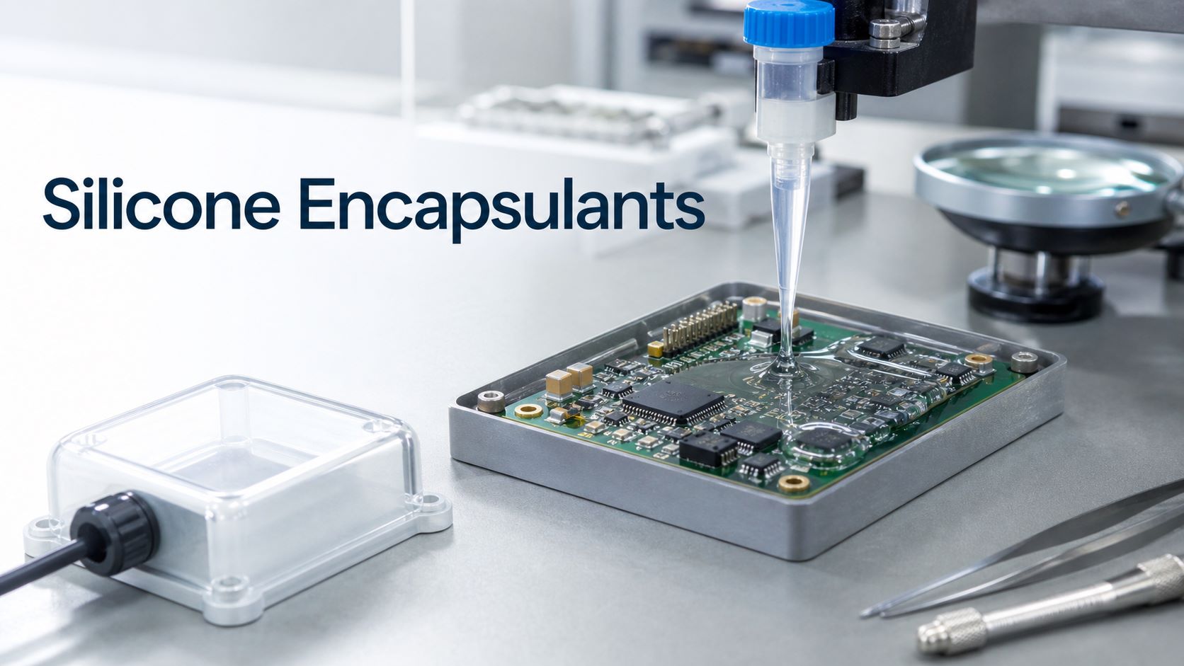
What Are Silicone Encapsulants for Electronics?
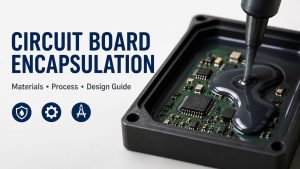
Silicone encapsulants for electronics are protective materials used to cover or surround electronic components, PCB assemblies, sensors, connectors, power modules, LED modules, and other electronic parts. After curing, the silicone forms a flexible protective layer or mass around the circuit.
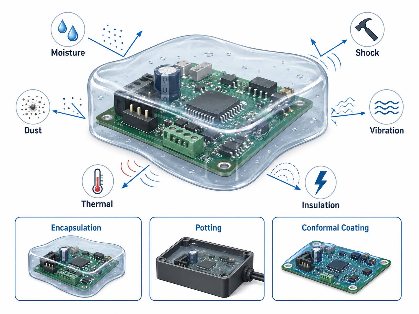
The main purpose is to protect electronics from environmental and mechanical stress.
Silicone encapsulants may help protect against:
| Risk | Why It Matters |
|---|---|
| Moisture | Reduces corrosion and leakage risk |
| Vibration | Helps absorb mechanical stress |
| Shock | Protects components from impact |
| Thermal cycling | Handles expansion and contraction |
| Dust and contamination | Reduces exposure to particles |
| Electrical stress | Improves insulation where suitable |
In electronics manufacturing, silicone encapsulants are often discussed together with PCB potting, PCB encapsulation, conformal coating, and electronic sealing. These terms are related, but they are not always the same.
Encapsulation usually means the electronic parts are covered or surrounded by a protective material. Potting usually means the assembly is placed in a housing or cavity and filled with a compound. Conformal coating is usually a thinner protective coating over the PCBA surface.
When Should Electronics Use Silicone Encapsulants?
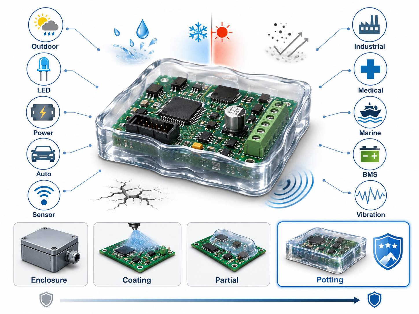
Electronics should use silicone encapsulants when the PCB assembly needs protection that a normal solder mask, enclosure, or conformal coating cannot fully provide.
Typical use cases include:
- Outdoor electronics
- LED lighting modules
- Power electronics
- Automotive electronics
- Sensor modules
- Industrial control boards
- Medical device electronics
- Marine or humid-environment electronics
- Battery management systems
- High-vibration equipment
Silicone encapsulants are especially useful when the product faces vibration, shock, moisture, or temperature changes. Compared with rigid materials, cured silicone is usually more flexible, which can reduce stress on components and solder joints.
However, silicone encapsulation is not always necessary. It can add cost, weight, process time, rework difficulty, and inspection complexity. Before choosing silicone encapsulants, engineers should confirm the real working environment and reliability requirement.
A practical question is not only “Can we pot this board?” but “Does this board need potting, conformal coating, partial encapsulation, sealing, or only better enclosure protection?”
Silicone Encapsulants vs Epoxy and Polyurethane
Silicone, epoxy, and polyurethane are common encapsulation or potting material families in electronics. Each material has different strengths and limitations.
| Material | Typical Strength |
| Silicone | Flexible, thermal cycling, vibration resistance |
| Epoxy | Hard, strong mechanical protection |
| Polyurethane | Balanced flexibility and protection |
Silicone encapsulants are often selected when flexibility, temperature cycling, and stress relief matter. They are useful for assemblies where components, solder joints, and substrates may expand and contract during operation.
Epoxy can provide strong mechanical protection, but it is usually harder and may create higher stress on components. It can also make rework very difficult.
Polyurethane can be a middle option in some projects, but material behavior depends strongly on formulation.
For PCB and PCBA projects, the best choice depends on:
- Product environment
- Temperature range
- Vibration level
- Moisture exposure
- Heat dissipation needs
- Component sensitivity
- Rework expectations
- Testing and inspection method
- Cost and production volume
EBest Circuit does not choose a material based only on the material name. The protection method should match the real product use environment and manufacturing process.
Silicone Encapsulants for PCB Potting and Encapsulation
Silicone encapsulants for electronics are often used in PCB potting and PCB encapsulation when a board needs more protection than standard assembly.
- In PCB potting, the assembled board is usually placed inside a housing or cavity, and the potting compound is poured or dispensed around the assembly. After curing, the material helps protect the board from moisture, vibration, and mechanical stress.
- In PCB encapsulation, the protective material may cover a selected area, component group, module, or full assembly depending on the product requirement.
Common applications include:
| PCB/PCBA Type | Why Encapsulation May Help |
| LED modules | Moisture and thermal cycling protection |
| Sensor boards | Environmental sealing |
| Power boards | Insulation and vibration resistance |
| Outdoor PCBA | Dust and moisture protection |
| Automotive modules | Shock and temperature cycling |
| Industrial controls | Harsh environment reliability |
For customers, the key is to define the protection requirement early. If potting or encapsulation is added after the PCB layout, enclosure, connector choice, and testing method are already fixed, some risks may be harder to solve.
Important details include connector exposure, test point access, heat-generating components, board cleanliness, housing clearance, material height, and curing process.
Thermal Management with Silicone Encapsulants for Electronics
Thermal management is an important consideration when using silicone encapsulants for electronics. Some silicone encapsulants are designed mainly for environmental protection, while others are formulated with thermally conductive fillers to help transfer heat.
For power electronics, LED boards, automotive modules, battery systems, and high-current PCBA, heat should be reviewed before encapsulation.
Key thermal questions include:
| Question | Why It Matters |
| Which components generate heat? | Identifies hot spots |
| Where does heat need to go? | Defines thermal path |
| Is the encapsulant thermally conductive? | Affects heat transfer |
| Is the enclosure part of heat dissipation? | Impacts structure |
| Are thermal vias or copper areas needed? | Supports PCB heat spreading |
Silicone encapsulation can protect electronics, but it can also change the thermal behavior of the assembly. If heat is trapped around sensitive components, reliability may be affected.
For this reason, engineers should review PCB copper thickness, thermal vias, metal core substrate options, ceramic PCB options, component spacing, and enclosure design before finalizing a potting or encapsulation process.
EBest Circuit can help review PCB manufacturing and PCBA assembly factors that affect thermal reliability, such as copper thickness, material selection, board structure, soldering process, component placement constraints, and inspection requirements.
Moisture, Vibration, and Shock Protection in Electronics Potting
Electronics potting is often used when the PCBA must survive a more difficult environment than a normal indoor device.
Moisture can cause corrosion, leakage current, insulation failure, and long-term reliability problems. Vibration can stress solder joints, connectors, and larger components. Shock can damage components or break weak mechanical points.
Silicone encapsulants can help because cured silicone is generally flexible and resilient. It can absorb movement better than very rigid materials in many applications.
Protection areas may include:
- Connector-adjacent zones
- Power components
- Sensor areas
- Wire bonding or delicate interconnects
- LED assemblies
- High-vibration module areas
- Outdoor exposed electronics
But potting is not a cure for every design or assembly risk. If a connector is not sealed correctly, if board cleaning is poor, if components are not suitable for the temperature range, or if the enclosure traps water, encapsulation alone may not solve the reliability issue.
Good protection starts before potting. The PCB, components, assembly process, cleaning requirement, enclosure, and inspection method should all be reviewed together.
How to Choose Customized Silicone Encapsulant for Electronics
A customized silicone encapsulant for electronics should be selected based on the actual product requirement, not only the phrase “silicone potting compound.”
The selection should consider:
| Factor | What to Check |
| Hardness | Stress on components |
| Viscosity | Flow and filling ability |
| Cure method | Production process fit |
| Thermal conductivity | Heat transfer requirement |
| Dielectric property | Electrical insulation |
| Temperature range | Product operating condition |
| Adhesion | Bonding to PCB and housing |
| Reworkability | Repair or failure analysis needs |
For example, a low-viscosity silicone may flow more easily around components and into small gaps. A thermally conductive silicone may be needed when heat transfer is important. A softer material may help reduce mechanical stress, but it may not provide the same rigidity as harder compounds.
Engineers should also confirm material compatibility with the PCB surface finish, solder mask, components, connectors, wires, labels, and enclosure material.
For PCBA production, the encapsulant choice also affects dispensing, curing, inspection, packaging, and testing. This is why the material decision should be made together with the manufacturing process.
PCB Assembly Checks Before Silicone Encapsulation
Before silicone encapsulation, PCB assembly quality must be checked carefully. Once a board is potted or encapsulated, rework and inspection become more difficult.
Important checks include:
| Check | Why It Matters |
| Solder joint quality | Defects may be hidden after potting |
| Board cleanliness | Residue may affect reliability |
| Component height | Impacts filling and clearance |
| Connector protection | Avoids blocked mating areas |
| Test point access | Testing may be harder later |
| Functional testing | Finds issues before encapsulation |
| Packing method | Prevents damage after curing |
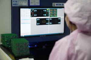
For SMT assembly, BGA, fine-pitch ICs, connectors, and sensor-related areas should be inspected before encapsulation. If X-ray, AOI, visual inspection, or functional testing is required, it should be done before the material covers the board.
Cleaning is also important. Flux residue, solder balls, dust, oil, or other contamination can create problems after encapsulation. If the customer has cleanliness requirements, those requirements should be defined before production.
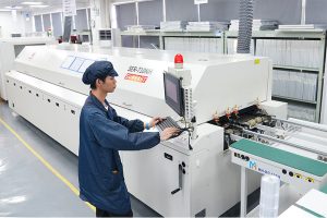
EBest Circuit supports DFM review, SMT assembly, inspection, testing coordination, and process review for PCBA projects that include coating, potting, or encapsulation-related requirements.
Silicone Encapsulants for Electronics Case Study
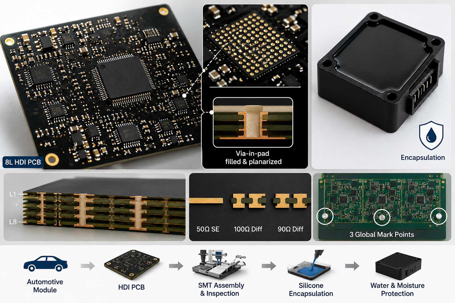
A U.S. customer needed an 8-layer HDI PCB for an automotive electronic module that would later use silicone encapsulation for moisture protection.
The key point was clear: silicone encapsulation can protect the assembly, but it cannot fix PCB fabrication, soldering, or cleanliness issues that are already sealed inside the module.
EBest Circuit manufactured the PCB with:
- 0.97mm FR4, Tg170
- L1-L2 and L7-L8 blind vias
- L2-L7 buried vias
- 0.10mm minimum holes
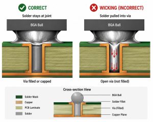
- Resin-filled and planarized via-in-pad in the BGA area
- 50 ohm, 90 ohm, and 100 ohm controlled impedance
- ENIG with 1uin gold
- Three global fiducial marks on the panel for SMT alignment
The resin-filled BGA via-in-pad structure helped create a flatter soldering surface. Controlled impedance supported signal stability, while panel fiducials improved solder paste printing, component placement, and inspection accuracy before encapsulation.
For this project, silicone provided the environmental barrier. The HDI PCB fabrication and PCBA process control provided the reliable foundation underneath it.
EBest Circuit can review HDI structures, BGA via-in-pad, impedance requirements, panel design, and SMT notes before a PCB assembly moves into silicone potting, partial encapsulation, or conformal coating.
Why Choose EBest Circuit for Encapsulated PCB and PCBA Projects?
EBest Circuit (Best Technology) supports encapsulated PCB and PCBA projects as part of a complete PCB and PCBA manufacturing service. We do not position silicone encapsulation as a standalone material-selling service. Instead, we help customers review whether the PCB fabrication, assembly process, inspection plan, and protection requirement can work together.
Our support may include:
- PCB fabrication
- Component sourcing
- SMT assembly
- DFM review
- PCBA inspection
- Functional testing coordination
- Conformal coating support
- Potting-related process support
- Packing and delivery planning
- Engineering review before production
This matters because encapsulation affects more than the final protection layer. It can affect component selection, connector access, testing, heat dissipation, cleaning, repairability, and final inspection.
EBest Circuit has over 20 years of PCB and PCBA experience and supports FR4 PCB, HDI PCB, metal core PCB, ceramic PCB, flexible PCB, rigid-flex PCB, component sourcing, and PCBA assembly. For customers developing outdoor electronics, LED modules, power electronics, sensors, industrial controls, medical electronics, and high-reliability modules, this one-stop support helps reduce handoff risk between PCB manufacturing, assembly, and protection requirements.
FAQs about Silicone Encapsulants for Electronics
1. What are silicone encapsulants for electronics used for?
Silicone encapsulants for electronics are used to protect PCB assemblies, components, sensors, modules, and power electronics from moisture, vibration, shock, dust, contamination, and thermal cycling.
2. Are silicone encapsulants the same as conformal coating?
No. Conformal coating is usually a thin protective layer over the PCB surface. Silicone encapsulation or potting is usually thicker and provides more mechanical and environmental protection.
3. Is silicone better than epoxy for PCB potting?
It depends on the product. Silicone is usually more flexible and better for thermal cycling and vibration. Epoxy is usually harder and stronger mechanically, but it may create more stress and make rework difficult.
4. Can silicone encapsulation help with heat dissipation?
Some silicone encapsulants are thermally conductive and can help transfer heat. However, thermal performance depends on the material, PCB copper design, thermal vias, component layout, enclosure, and heat path.
5. What should be checked before PCB encapsulation?
Before PCB encapsulation, check solder joint quality, board cleanliness, component placement, connector areas, test point access, functional testing, curing process, and packing requirements.
6. Can EBest Circuit help with PCB and PCBA projects that use silicone encapsulants?
Yes. EBest Circuit can support PCB fabrication, component sourcing, SMT assembly, DFM review, inspection, testing coordination, and potting-related production review for PCB and PCBA projects that require additional protection. Please send your Gerber files, BOM, drawings, protection requirements, and product use environment to sales@bestpcbs.com for review.
If your PCB or PCBA project needs protection from moisture, vibration, shock, thermal cycling, or harsh operating environments, please feel free to contact sales@bestpcbs.com. EBest Circuit’s engineering team can help review the PCB manufacturing, assembly, testing, and protection path before production starts.