PCB manufacturing PCB manufacturing
Home > Blog

parts of a pcb

Parts of a PCB: Components, Functions, and Identification
Tuesday, July 21st, 2026

The parts of a PCB include two distinct groups: the physical features built into the bare board and the electronic devices assembled on its surface. Keeping these groups separate is the fastest way to understand a circuit board, identify unfamiliar parts, and communicate accurately with a PCB or PCBA supplier.

A green board with chips and connectors is often called a PCB in everyday conversation. Technically, however, the bare board becomes a printed circuit board assembly, or PCBA, after components are soldered onto it. The distinction matters when you prepare fabrication files, purchase components, troubleshoot a failure, or request a quotation.

This guide explains the board structure, common component names, functions, reference designators, mounting methods, specialized layouts, and the basic PCB design workflow. It is written for readers who need practical recognition skills rather than a component-theory textbook.
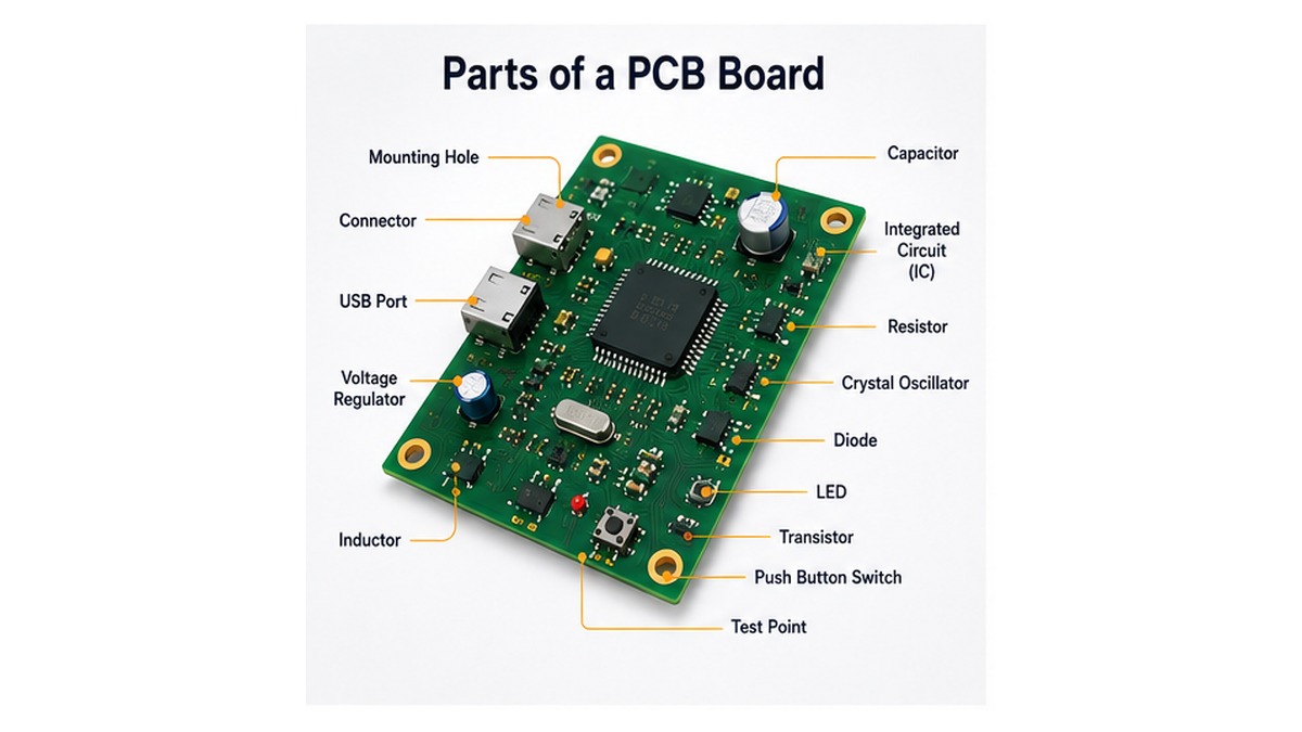
Parts of a PCB board diagram identifying the mounting holes, connectors, integrated circuit, resistor, capacitor, inductor, diode, LED, transistor, crystal oscillator, test point, and voltage regulator

What Are the Main Parts of a PCB?

The phrase “PCB parts” can refer to the board itself or to the components installed on it. A complete explanation should include both.

Category Typical Parts Main Purpose
Bare-board structure Core, prepreg, copper layers, solder mask, silkscreen, surface finish Provides mechanical support, electrical insulation, conductor patterns, protection, and readable markings.
Conductive features Traces, planes, pads, vias, plated holes, copper pours, edge fingers Carry power and signals and create electrical connection points.
Electronic components Resistors, capacitors, inductors, diodes, transistors, ICs, crystals, sensors Control current, store energy, process information, switch loads, and sense conditions.
Interconnection parts Headers, sockets, USB ports, terminal blocks, board-to-board connectors Link the board to power sources, cables, modules, displays, motors, antennas, or other boards.
Mechanical and thermal parts Mounting holes, standoffs, shields, clips, heatsinks, thermal pads Secure the assembly, control heat, and protect sensitive circuitry.
Test and service features Test points, jumpers, programming headers, fiducials, probe pads Support assembly alignment, programming, measurement, inspection, and repair.

The board features create the electrical “road system.” The mounted components are the devices that use those roads to perform a function. A board without components can still be inspected electrically, but it cannot perform the intended product function until assembly is complete.

PCB Board Structure: Substrate, Copper, Pads, Vias, Solder Mask, and Silkscreen
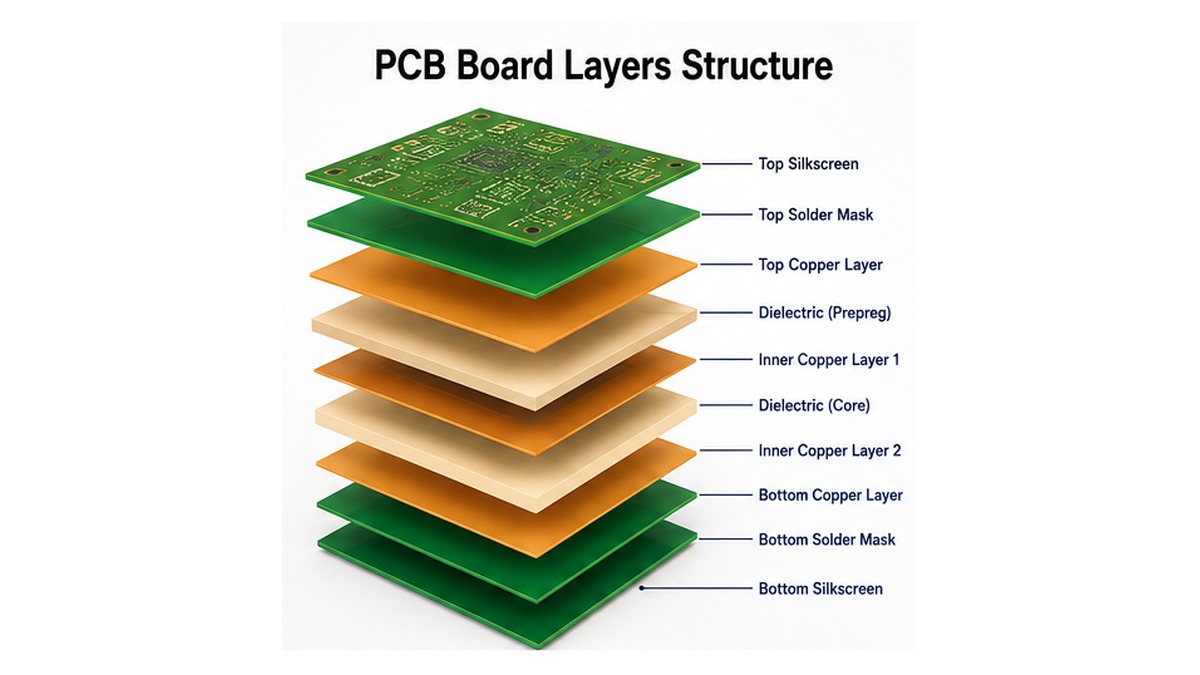
Exploded PCB board layers structure showing top silkscreen, solder mask, copper layers, prepreg, core, inner copper layers, and bottom silkscreen

A PCB is a laminated stack of insulating and conductive materials. The exact structure changes with the layer count, impedance requirement, voltage, heat load, flexibility, and manufacturing process, but the principal features remain recognizable.

Substrate, Core, and Prepreg

The substrate provides rigidity and electrical insulation. FR-4 glass-reinforced epoxy is common in industrial and consumer electronics, while flexible circuits use polyimide and high-frequency boards may use low-loss laminates. In a multilayer board, cured core material and partially cured prepreg bond the copper layers into one structure.

Copper Traces and Planes

Traces are patterned copper conductors that route signals or current between pads. Planes and copper pours cover larger areas and commonly distribute ground, power, or heat. Their width, thickness, spacing, reference plane, and return path influence current capacity, impedance, noise, and temperature rise.

Pads, Plated Holes, and Vias

  • SMD pads receive the terminations of surface-mount devices.
  • Through-hole pads surround drilled holes used by leads, pins, or mechanical hardware.
  • Vias connect copper between layers. Common types include through vias, blind vias, buried vias, and laser-drilled microvias.
  • Via-in-pad structures place a via directly inside a component pad and usually require filling and planarization for reliable assembly.

Solder Mask, Silkscreen, and Surface Finish

Solder mask covers most exposed copper and helps control solder placement while protecting the circuit surface. Silkscreen adds reference designators, polarity marks, connector labels, revision codes, and other readable information. The surface finish protects uncovered copper pads and provides a solderable interface; common choices include HASL, ENIG, immersion silver, immersion tin, and ENEPIG.

Practical distinction: solder mask is not the electrical insulator between internal copper layers. Core and prepreg provide that dielectric function; solder mask is a thin outer protective coating.

PCB Components List with Pictures and Functions
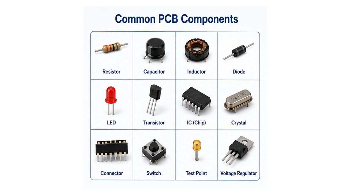
Common PCB components with pictures including resistor, capacitor, inductor, diode, LED, transistor, integrated circuit, crystal, connector, switch, test point, and voltage regulator

The table below is a practical PCB parts list. The reference letters are common conventions, but company libraries may use alternatives. The BOM and schematic remain the authoritative documents.

Component Common Designator Function Visual Identification Clues
Resistor R Limits current, divides voltage, sets bias, provides pull-up or pull-down paths, and terminates signals. Small rectangular SMD body or axial through-hole body with color bands. Larger current-sense parts may be metallic and marked with low resistance values.
Capacitor C Stores charge, filters noise, stabilizes power rails, couples AC signals, and supports timing networks. Small tan or dark SMD blocks, cylindrical aluminum electrolytics, molded tantalum packages, or film boxes. Polarized types have a polarity mark.
Inductor L Stores energy in a magnetic field and filters current in converters, RF networks, and power inputs. Coil, ferrite bead, molded block, or shielded square package. Power inductors are often among the tallest SMD parts.
Diode D Controls current direction, rectifies AC, clamps voltage, protects against reverse polarity, or suppresses transients. Two-terminal package with a stripe or line indicating the cathode. TVS diodes may resemble small IC packages.
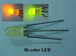
LED LED or D Emits light for status indication, illumination, optical sensing, or communication. Clear or colored through-hole lens, white SMD package, or compact multicolor package. Polarity must be observed.
Transistor or MOSFET Q Switches or amplifies electrical signals and controls motors, LEDs, relays, converters, and processor power rails. Usually 3 or more terminals. Packages range from tiny SOT styles to large power packages with exposed thermal tabs.
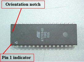
Integrated circuit U or IC Performs processing, memory, communication, sensing, regulation, amplification, or dedicated control functions. Black molded package with pins, gull-wing leads, bottom pads, or solder balls. A dot, notch, or chamfer identifies pin 1.
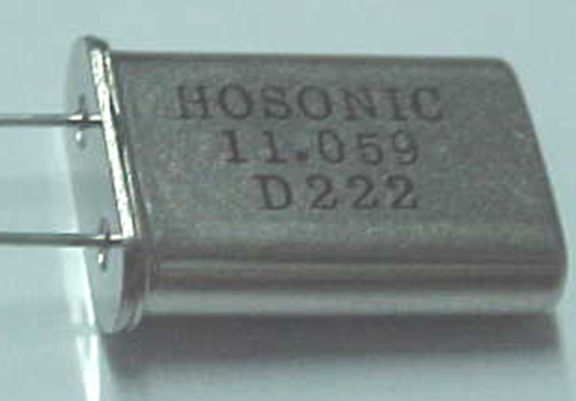
Crystal or oscillator Y or X Provides a stable clock or reference frequency for processors, radios, interfaces, and timers. Metal can, ceramic SMD rectangle, or small oscillator module. Frequently located close to an MCU, FPGA, RF IC, or USB controller.
Transformer T or TR Transfers energy or signals through magnetic coupling and may provide isolation or voltage conversion. Wound core or molded package. Ethernet magnetics may be integrated inside a connector.
Relay K, RLY, or RL Uses an electrical control signal to open or close isolated mechanical contacts. Rectangular plastic housing, often with a printed coil voltage and contact rating. Requires more board area than semiconductor switches.
Fuse F Opens the circuit when current exceeds a safe level. Glass cartridge, ceramic tube, polymer resettable fuse, or compact SMD body. A fuse should not be replaced with a higher rating without analysis.
Connector J, P, or CN Connects power, signals, cables, modules, displays, sensors, or another circuit board. Header pins, sockets, edge connectors, USB ports, terminal blocks, FFC connectors, coaxial connectors, or board-to-board arrays.
Switch or button SW or S Provides manual input, configuration, reset, mode selection, or power control. Tactile dome, slide switch, rocker, rotary encoder, DIP switch, or membrane contact area.
Sensor U, S, TH, or application-specific Measures temperature, pressure, light, motion, magnetic field, current, humidity, sound, or other conditions. Appearance varies widely. Open ports, optical windows, exposed thermal pads, or MEMS packages may indicate the sensing function.
Test point TP Provides a controlled location for probes, fixtures, programming, calibration, or production testing. Exposed round or rectangular pad, loop terminal, or plated post with a nearby TP label.

A visually similar package can contain very different internal functions. For example, a 6-pin SOT package may be a regulator, logic gate, sensor interface, or protection array. Package recognition narrows the possibilities; it does not prove the exact part number.

How Do You Identify PCB Components on a Circuit Board?

Reliable identification uses several clues together. A good process starts with non-destructive observation and moves toward documentation and measurement.

  1. Read the reference designator. Labels such as R12, C8, U3, or J1 reveal the component family and its unique location number.
  2. Inspect the package. Count pins, note the body dimensions, and identify whether the part is axial, radial, leaded, leadless, BGA, QFN, SOIC, SOT, connector, or custom mechanical hardware.
  3. Record the top marking. ICs often show a shortened code rather than the complete orderable part number. Photograph it under controlled lighting and search the marking together with the package and manufacturer logo.
  4. Check polarity and orientation. Look for pin-1 dots, notches, diode bands, electrolytic capacitor stripes, LED cathode marks, and PCB silkscreen symbols.
  5. Study the nearby circuit. A component beside an inductor and several ceramic capacitors may belong to a switching regulator. A crystal close to a microcontroller is probably part of its clock circuit.
  6. Confirm with documentation. Use the schematic, BOM, assembly drawing, pick-and-place file, approved vendor list, or original product service manual.
  7. Measure only when appropriate. Resistance, diode drop, capacitance, continuity, and rail voltage can provide evidence, but in-circuit measurements may be altered by parallel paths. De-energize the board before passive resistance or continuity checks.
Important: do not power an unknown or visibly damaged board merely to identify a component. Check for shorts, contamination, reversed parts, burnt areas, and incorrect supply polarity first.

Common Reference Designators

Designator Usually Means Useful Identification Detail
R Resistor Value may be printed as a 3-digit, 4-digit, or EIA-96 code on larger SMD packages.
C Capacitor Small ceramic capacitors are often unmarked; the BOM or measurement is usually required.
L / FB Inductor / ferrite bead Ferrite beads may look like resistors but are used mainly for high-frequency noise suppression.
D / LED Diode / light-emitting diode Orientation is critical. Confirm the board symbol and package mark.
Q Transistor or MOSFET Nearby gate resistors, drivers, inductors, or loads help reveal the role.
U / IC Integrated circuit Read the complete marking, logo, pin count, package, and pin-1 indicator.
J / P / CN Connector The schematic net names usually explain whether it carries power, communication, or general I/O.
Y / X Crystal or oscillator Frequency may be printed directly on the package.
F Fuse Check rated current, voltage, speed, interrupt rating, and whether it is resettable.
TP Test point A test procedure or net label is needed to understand the expected signal.

Surface-Mount and Through-Hole Parts: What Is the Difference?

Surface-mount technology attaches component terminals directly to pads on the board surface. Through-hole technology inserts leads or pins into drilled holes and solders them on the opposite side or inside a plated barrel. Modern PCB assemblies frequently combine both.

Comparison Surface-Mount Device Through-Hole Part
Board density Supports compact packages and placement on both sides. Consumes more board area because of drilled holes and lead spacing.
Assembly method Well suited to stencil printing, automated placement, and reflow soldering. Often assembled by insertion, selective soldering, wave soldering, or hand soldering.
Electrical behavior Short terminals can reduce unwanted inductance and capacitance at high frequencies. Longer leads may add parasitic effects but can be acceptable in many low-frequency or power applications.
Mechanical loading Strong enough for most components when land patterns and solder joints are designed correctly. Often preferred for connectors, switches, large transformers, and parts exposed to repeated mechanical force.
Repair access Small or leadless packages may require hot air, preheating, magnification, or X-ray inspection. Large leaded parts are usually easier to probe and replace manually.
Typical examples Chip resistors, ceramic capacitors, QFN ICs, BGAs, SOT transistors, compact LEDs. Pin headers, terminal blocks, large electrolytics, transformers, relays, power connectors.

The selection is not simply “new versus old.” It is an engineering decision based on space, volume, assembly process, current, heat, vibration, serviceability, component availability, and expected mechanical stress.

How Do PCB Parts Work Together in Functional Circuit Sections?

Components are easier to understand when they are grouped by circuit function instead of viewed as isolated packages. Most boards contain several recognizable zones.

  • Input protection: connector, fuse, TVS diode, reverse-polarity device, common-mode choke, and filtering capacitors.
  • Power conversion: regulator IC, MOSFET, inductor, diode, feedback resistors, and input/output capacitors.
  • Processing and control: MCU, FPGA, processor, memory, reset circuit, decoupling capacitors, and programming header.
  • Clock generation: crystal or oscillator, loading capacitors, and short controlled traces to the clock pins.
  • Analog signal conditioning: op-amps, precision resistors, filters, references, ADCs, DACs, and sensor interfaces.
  • Communication: transceiver ICs, termination resistors, isolation devices, ESD protection, magnetics, and connectors.
  • Load driving: MOSFETs, gate drivers, relays, flyback diodes, current-sense resistors, and output terminals.
  • Test and calibration: test points, jumpers, trim components, debug headers, and fixture contacts.

Placement often reveals these zones. Decoupling capacitors sit close to IC power pins. High-current paths use wider copper and cluster near power devices. Sensitive analog circuitry is commonly separated from switching nodes, motors, and fast digital interfaces. Connectors usually define where power and signals enter or leave the assembly.

How Do You Build a PCB Parts List from the Schematic and BOM?

A PCB parts list should not be reconstructed from photographs unless the original documentation is unavailable. The correct source is the approved design database and BOM.

  1. Start with the schematic. Verify that every placed symbol has a reference designator, value, manufacturer part number, and correct electrical connections.
  2. Check the footprint. Confirm package dimensions, pad geometry, pin numbering, thermal pad, courtyard, orientation, and assembly process.
  3. Generate the BOM. Group identical parts without losing location references. A useful BOM includes quantity, designators, description, manufacturer, manufacturer part number, package, rating, tolerance, lifecycle status, and approved alternatives.
  4. Review polarized parts. Diodes, LEDs, electrolytic capacitors, ICs, batteries, connectors, and some sensors need clear orientation control.
  5. Validate supply risk. Check stock, lead time, minimum order, moisture sensitivity, packaging format, compliance, and whether alternates are truly pin- and performance-compatible.
  6. Cross-check assembly data. The BOM, centroid file, assembly drawing, stencil data, and PCB revision must all describe the same product revision.
Recommended BOM Field Example Reason
Reference designators R12, R18, R24 Links the purchased line item to exact PCB locations.
Manufacturer part number Exact orderable code Prevents ambiguity caused by generic descriptions.
Electrical value and rating 10 kΩ, 1%, 0.1 W Defines the performance requirement.
Package 0603, QFN-32, SOT-23 Must match the land pattern and assembly capability.
Approved substitute Validated alternate MPN Supports continuity without uncontrolled substitution.
Do-not-populate status DNP / DNI Prevents optional or tuning positions from being assembled accidentally.
Lifecycle and compliance Active, RoHS, REACH Reduces redesign risk and supports product requirements.

What Are the Basic Steps of PCB Design?
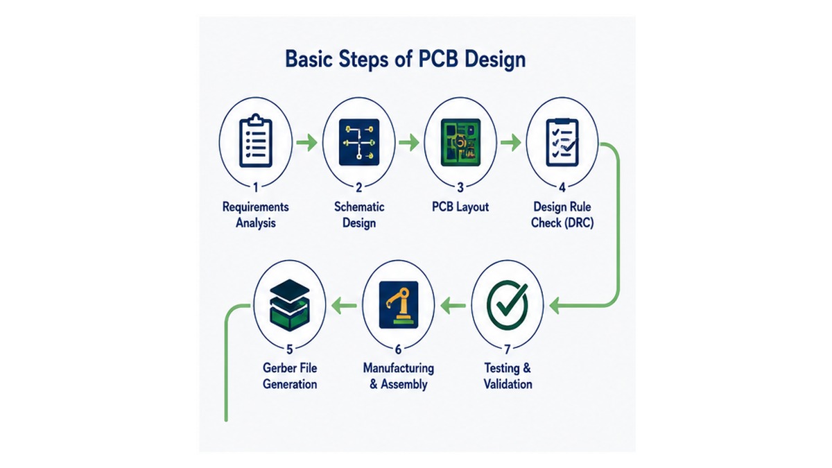
Basic steps of PCB design from requirements analysis and schematic design through PCB layout, design rule checking, Gerber generation, manufacturing, assembly, testing, and validation

PCB design converts product requirements into a manufacturable and testable assembly. The exact process varies by organization, but the core sequence is stable.

  1. Define requirements. Establish interfaces, supply rails, current, voltage, frequency, mechanical envelope, environment, compliance, cost, expected volume, and test strategy.
  2. Select components. Choose active and passive parts based on performance, availability, lifecycle, package, thermal behavior, and assembly constraints.
  3. Create and review the schematic. Add power architecture, signal conditioning, protection, decoupling, connectors, programming access, net labels, and design notes. Run electrical rule checks.
  4. Build the layer stack and rules. Define board thickness, copper weights, dielectric materials, controlled impedance, clearances, via structures, creepage, and manufacturing limits.
  5. Place components. Start with connectors, mechanical constraints, critical ICs, power stages, memory, clocks, and high-speed interfaces. Place support components close to the pins they serve.
  6. Route and pour copper. Protect return paths, separate noisy and sensitive circuits, control differential pairs, size current paths, and connect power and ground planes intelligently.
  7. Verify the design. Run design rule checks, review 3D fit, check signal and power integrity where required, evaluate thermal paths, and conduct DFM/DFA/DFT reviews.
  8. Generate production files. Release Gerber or ODB++/IPC-2581 data, drill files, netlist, fabrication drawing, stackup, BOM, centroid file, assembly drawings, stencil information, and test requirements.
  9. Prototype, assemble, and test. Inspect the bare board, assemble components, perform AOI or X-ray where appropriate, program firmware, run electrical and functional tests, and feed findings back into the next revision.

A clear component library and disciplined revision control connect every stage. A correct schematic with an incorrect footprint can still fail, and a correct layout paired with the wrong BOM revision can still produce the wrong assembly.

Frequently Asked Questions About PCB Parts

1. What is a PCB and what components does it contain?

A PCB is an insulating board with patterned copper conductors, pads, vias, coatings, and markings. When components such as resistors, capacitors, ICs, connectors, and switches are assembled onto it, the result is a PCBA.

2. What are the main parts of a PCB board?

The main bare-board parts are the substrate or core, dielectric layers, copper traces and planes, pads, vias, plated holes, solder mask, silkscreen, surface finish, board outline, and mounting features.

3. How can I identify an unknown PCB component?

Read its reference designator, package shape, top marking, pin count, polarity mark, and nearby circuit. Then confirm the result with the schematic, BOM, assembly drawing, datasheet, or service documentation.

4. What is the difference between a PCB and a PCBA?

A PCB is the fabricated bare board. A PCBA is the assembled board after electronic and mechanical parts have been placed and soldered.

5. Can capacitor values be identified by appearance?

Large electrolytic and film capacitors usually carry readable values. Small multilayer ceramic capacitors are often unmarked, so the BOM, schematic, or an appropriate measurement is required. In-circuit measurement may be affected by parallel components.

6. What information belongs in a PCB parts list?

Include quantity, reference designators, description, value, tolerance, rating, package, manufacturer, manufacturer part number, approved alternates, lifecycle status, assembly notes, and do-not-populate status where applicable.

7. Do keyboard and GPU PCBs use the same basic parts?

Yes. Both use copper features, vias, resistors, capacitors, ICs, connectors, and test points. Their layout priorities differ: keyboards focus on switch geometry and matrix scanning, while GPUs focus on high-current power delivery, high-speed memory routing, and thermal control.

8. How can this guide be saved as a PDF?

Open the HTML file in a modern browser, choose Print, and select “Save as PDF.” The print stylesheet removes shadows and formats tables for a cleaner document.

Need a manufacturability review or PCB/PCBA quotation? EBest Circuit can review your Gerber files, BOM, centroid data, stackup, and assembly requirements. Contact sales@bestpcbs.com.

You may also like

What are Parts of a PCB and Their Functions?
Wednesday, October 1st, 2025

Parts of a PCB form the backbone of every electronic product. In this blog, we break down the essential parts of a PCB, explain their types and functions, guide readers on component identification and reading reference designators, explore copper layers and the PCBA process, and etc.

Do you face the following dilemmas?

You’ll find effective solutions below:

  • Adopt advanced inspection technologies: To address PCB defect detection issues, image processing and machine learning techniques can be used for PCB defect detection and classification.
  • Provide detailed PCB component identification guides: To help customers better identify and understand components on a PCB, the detailed guides can be offered by EBest Circuit (Best Technology), including component types, functions, and identification methods.
  • Optimize PCB manufacturing and assembly processes: By adopting advanced soldering techniques and automated assembly equipment, the reliability and performance of PCBs can be significantly improved.
  • Offer customized PCB design and manufacturing services: Provide personalized PCB design and manufacturing solutions based on the customer’s specific requirements and application scenarios.

As a leading PCB board and PCBA factory, we manufacture and sell several types of PCB, such as single sided rigid PCB, rigid-flexible PCB, flexible PCB, Bluetooth module PCB, IMS PCB, copper MCPCB, AlN PCB, ceramic PCB assembly, and box build service. If you have any PCB fabrication or assembly service, just contact our sales team at sales@bestpcbs.com. Kindly be assured that there is no MOQ for our PCBs. We have worked in the PCB industry for nearly 2 decades. We have the whole experience to tackle your issues and provide you with practical solutions.

parts of a pcb

What are Parts of a PCB?

You will learn the parts of a PCB from two aspects: the physical structure of the board and the electronic components mounted on it. By understanding both, you will not only see how a printed circuit board works, but also understand how these parts interact to create reliable, functional devices.

1. The Structural Parts of a PCB

Every PCB starts with a layered foundation that makes signal transmission possible. These layers are not just materials; they each serve a distinct purpose:

  • Substrate (Base Material): Usually fiberglass such as FR4. It gives the board mechanical strength and electrical insulation.
  • Copper Layer: Thin copper sheets form the traces, pads, and planes that carry current and signals.
  • Pads: Small exposed copper areas where components are soldered. Pads act as the anchor points between the board and devices.
  • Vias: Tiny drilled holes plated with copper that connect one copper layer to another. They allow signals to pass vertically inside multilayer boards.
  • Solder Mask: The protective colored coating (often green) that covers copper traces. It prevents oxidation and short circuits during soldering.
  • Silkscreen: Printed labels showing reference designators, pin 1 indicators, and helpful text. It works like a map for engineers and technicians.
  • Traces (Conductive Paths): Copper lines that route signals from one component to another. Their width and spacing directly affect performance, especially in high-speed circuits.

Together, these elements form the “skeleton” and “nervous system” of the PCB. Without them, no component could be mounted or connected properly.

2. The Electronic Components on a PCB

While the structure gives shape, the mounted components bring the circuit to life. These are the common ones you’ll find:

  • Resistors: Control current flow and set voltage levels.
  • Capacitors: Store and release charge, filter noise, and stabilize circuits.
  • Inductors: Work with capacitors in filters and manage energy in magnetic fields.
  • Diodes: Allow current to flow in one direction only, protecting circuits.
  • LEDs (Light Emitting Diodes): Convert electrical energy into light for indicators or displays.
  • Transistors: Switch or amplify signals, forming the core of logic and power control.
  • Integrated Circuits (ICs): Miniaturized circuits inside a single package, handling everything from memory to processing.
  • Connectors: Provide interfaces to other boards, cables, or systems.
  • Crystal Oscillators: Generate precise clock signals that keep digital systems in sync.

These components, when placed on the PCB structure, transform a simple board into a functional system. Whether it’s a smartphone, a computer GPU, or industrial equipment, the synergy between the base structure and these devices defines reliability and performance.

What are the Types of PCB Parts?

When talking about PCB parts, it is not only about the visible components on the board but also how these components are categorized in the electronics industry. Understanding the classification methods helps engineers, designers, and even buyers to select the right components for their projects. The most common classification approaches are explained below.

1. Classified by Manufacturing Industry – Components vs. Devices

In the electronics field, “components” and “devices” are differentiated by whether the manufacturing process changes the molecular composition of the material.

  • Components: Products that do not change their molecular structure during processing. Examples include resistors, capacitors, inductors, potentiometers, transformers, connectors, switches, quartz/ceramic elements, and relays.
  • Devices: Products where the material structure is altered, often produced by semiconductor manufacturers. Examples include diodes, transistors, field-effect transistors, optoelectronic devices, integrated circuits (ICs), as well as vacuum tubes and liquid crystal displays.

2. Classified by Circuit Function – Discrete vs. Integrated

From a circuit function perspective, PCB parts can be divided into discrete and integrated devices.

  • Discrete Devices: Independent parts with relatively simple functions, mainly for voltage or current control. This group includes resistors, capacitors, inductors, diodes, and transistors.
  • Integrated Devices: Known as integrated circuits (ICs). They combine complete circuit functions within one package, enabling complex processing or control tasks. Examples include memory chips and processors.

3. Classified by Operating Mechanism – Passive vs. Active

Another way to categorize PCB parts is based on whether they require an external power supply to function.

  • Passive Components: They operate without an external power source and only consume or transfer the input signal energy. Common passive parts include resistors, capacitors, inductors, and diodes.
  • Active Components: They need a power supply to operate. This category includes transistors, field-effect transistors, and integrated circuits, most of which are semiconductor-based.

4. Classified by Assembly Method – Through-Hole vs. Surface Mount

With the evolution of assembly technologies, component packaging and installation methods have changed significantly.

  • Through-Hole Components: Require drilled holes on the PCB. Their leads pass through the board and are soldered on the opposite side. They are often larger in size and found in traditional designs.
  • Surface Mount Components (SMDs): Mounted directly onto the PCB surface without the need for drilled holes. They are compact, lightweight, and compatible with automated manufacturing. Most modern electronic products use SMD technology.

5. Classified by Application Environment – Reliability Grades

The same component may come in different reliability grades depending on its intended use environment.

  • Consumer Grade: General reliability, cost-effective, commonly used in household electronics, entertainment devices, and office equipment.
  • Industrial Grade: Higher stability, designed for industrial control systems, transportation, and instrumentation. Price and performance are balanced.
  • Military Grade: Extremely high reliability, used in aerospace, defense, and medical systems, where performance is mission-critical. Prices can be many times higher than consumer-grade parts.

What are SMD Components?

SMD (Surface Mount Device) refers to electronic components specifically designed for surface mount technology (SMT). Unlike traditional through-hole components, SMDs have short or no leads and are soldered directly onto the surface of a printed circuit board (PCB). These components are fundamental to modern electronics, enabling high-density, miniaturized circuit designs used in smartphones, tablets, industrial control boards, automotive electronics, and more.

Common Types of SMD Components

  1. Chip Components
    • Chip Resistors (e.g., 0402, 0603, 0805 packages)
    • Chip Capacitors (ceramic, tantalum, etc.)
    • Chip Inductors (used for filtering or power circuits)
  2. Diodes and Transistors
    • SMD Diodes (e.g., Schottky diodes)
    • SMD Transistors
  3. Integrated Circuits (ICs)
    • QFP (Quad Flat Package): medium pin density ICs
    • BGA (Ball Grid Array): high-density ICs with solder balls on the bottom
    • QFN (Quad Flat No-lead): low-profile, excellent thermal performance
  4. Other SMD Devices
    • SMD LEDs
    • Micro Switches
    • SMD Crystals and Oscillators

SMD components are designed to support automated production. For instance, BGA chips have solder balls spaced typically within 0.5mm, requiring high-precision placement machines and advanced optical recognition systems for accurate mounting. Even smaller CSP packages with 0.3mm spacing often necessitate machine upgrades for proper handling.

SMT vs. SMD: Understanding the Difference

Although closely related, SMT and SMD are fundamentally different concepts:

  • SMT (Surface Mount Technology) is a complete production process. It replaces traditional through-hole assembly by mounting components directly on the PCB surface. SMT includes solder paste printing, high-speed component placement, and reflow soldering. Its main advantages are higher assembly efficiency, smaller PCB footprint, and support for high-density, high-precision layouts. For example, using 0201 SMD components in a smartwatch or smartphone PCB can reduce board size by about 40%, although it also increases the requirements for temperature- and humidity-controlled environments.
  • SMD (Surface Mount Device) is the actual component designed for SMT. SMDs feature metallic terminals or short leads that allow direct soldering on PCB pads. Their miniaturized design enables higher circuit integration. For example, a 0402 chip resistor measures only 1.0mm × 0.5mm and relies entirely on SMT machines for precise placement.

The development of SMD components drives SMT equipment upgrades, while high-precision SMT processes fully leverage the performance and miniaturization of SMDs. Together, they form the foundation of modern electronic manufacturing, ensuring reliable assembly, lower defect rates, and easier maintenance for high-density or complex boards.

In summary, SMT is the assembly method, while SMD is the component being assembled. Understanding this distinction is essential for optimizing production processes, improving product quality, and supporting the ongoing miniaturization and integration of electronic devices.

What Part of a PCB Contains Reference Designators?

Reference designators on a PCB are primarily found on component footprints and the silkscreen layer. A reference designator is a unique alphanumeric code assigned to each component on a PCB, such as R1 for a resistor, C3 for a capacitor, or U5 for an IC.

Purpose and Function:

  • Identifies each component uniquely for assembly, testing, and maintenance.
  • Facilitates communication between designers, manufacturers, and technicians.
  • Helps locate components during inspection, troubleshooting, or repair.

Physical Location and Visual Representation

  • Silkscreen Layer:
    Reference designators are typically printed on the top (and sometimes bottom) silkscreen layer, near the corresponding component pads. They are visible to the naked eye and guide assembly or manual inspection.
  • Component Footprints:
    Some CAD software embeds reference designators directly into the copper layer or mask layer for automated processes, especially for automated optical inspection (AOI) alignment.

Visual Details:

  • Usually small, clear alphanumeric text.
  • Placed adjacent to the component but without overlapping pads to avoid soldering issues.
  • May appear on both sides for double-sided PCBs.

How Reference Designators Are Generated

  • Automatically assigned in PCB design software (e.g., Altium, KiCad, Eagle) based on component type.
  • Typically follow a standardized convention:
    • R → Resistors
    • C → Capacitors
    • L → Inductors
    • D → Diodes
    • U → ICs
    • Q → Transistors
  • Designators can be manually adjusted if needed for clarity or specific assembly requirements.

Common Exceptions and Special Cases

  • High-Density Boards: Some very small SMD components may omit reference designators on the PCB due to space constraints.
  • Hidden or Buried Components: On multi-layer or high-density PCBs, inner layers or tightly packed components may not show designators physically; these are tracked digitally in the BOM (Bill of Materials).
  • Custom Markings: Some PCBs may include manufacturer-specific codes or omit standard designators for proprietary or security reasons.
  • Double-Sided Boards: Reference designators may appear on both top and bottom silkscreen layers for clarity.

Ultimately, reference designators exist mainly on the silkscreen layer and component footprints. They are alphanumeric codes uniquely identifying each component, guiding assembly, inspection, and maintenance. Their placement is carefully chosen for visibility, non-interference with soldering, and manufacturability. Exceptions occur in high-density boards, inner layers, or specialized designs, but the designators remain critical for PCB documentation and lifecycle management.

How to Read PCB Components Identification?

1. Core Identification Principles: Classify First, Then Inspect

  1. Check the Package Type: Determine whether the component is a through-hole (DIP) or a surface-mount (SMD) component. This guide focuses primarily on through-hole components.
  2. Observe Shape and Color: The component’s shape, size, and color provide the first clues for quick classification.
    • Green disc-like components → ceramic capacitors
    • Black cylindrical with white stripes → resistors
    • Black cylindrical with polarity marking → electrolytic capacitors
  3. Check Symbols and Silkscreen:
    • PCB markings: The board usually has silkscreened symbols (R, C, L, D, Q, U) and reference designators (e.g., R1, C5) to indicate the component type.
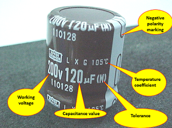
    • Component markings: Numbers, letters, or codes printed on the component indicate key parameters (resistance, capacitance, inductance) and specifications (tolerance, voltage rating, temperature coefficient).
  4. Check Polarity: For polarized components such as diodes, electrolytic capacitors, and ICs, correct polarity identification is crucial.
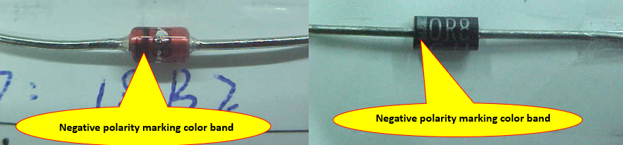
    • Diodes: The end with a white or black band is the cathode.
    • Electrolytic capacitors: The gray stripe indicates the negative lead, matching the PCB marking.
    • ICs: A notch or dot marks pin 1, typically located at the lower-left corner.

2. Detailed Methods for Key Components

1. Resistors (R)

  • Identification: Usually axial cylindrical with color bands or numeric markings.
  • Reading Parameters:
    • Color-coded resistors:
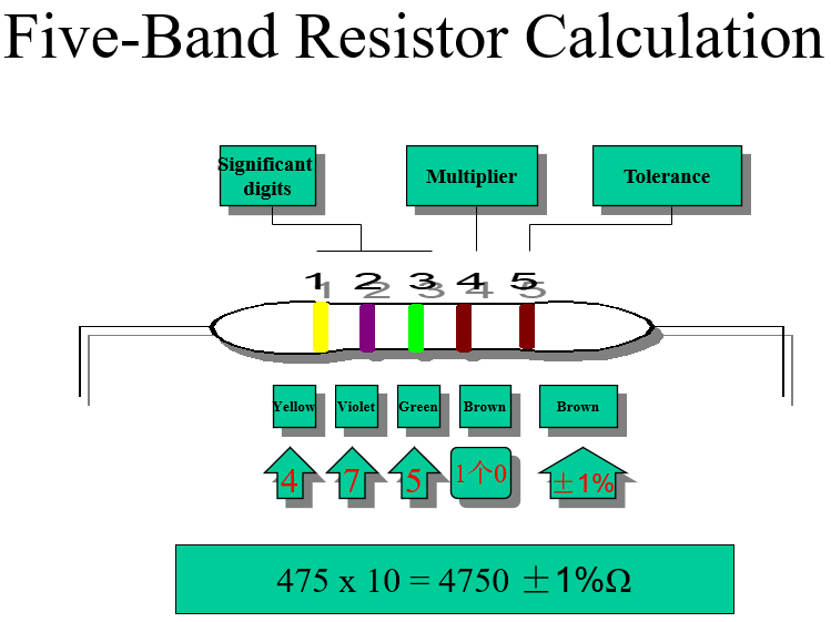
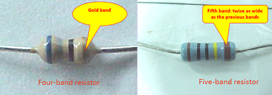
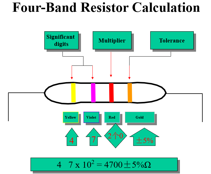
      • 4-band: First two bands = digits, third = multiplier, fourth = tolerance.
How to Read PCB Components Identification?
  • 5-band: First three bands = digits, fourth = multiplier, fifth = tolerance.
How to Read PCB Components Identification?
  • Reading direction: Start from the end closest to the gold/silver band or wider band.
How to Read PCB Components Identification?
  • Numeric codes: E.g., “102” = 10 × 10² Ω = 1 kΩ.
  • Special resistors: Varistors (voltage protection), thermistors (temperature sensing), potentiometers (adjustable), and fuses (sacrificial resistors).

2. Capacitors (C)

  • Identification: Based on shape and material.
    • Ceramic: Small, disc-shaped, brown or blue, non-polar, three-digit silkscreen code (e.g., 104 = 100 nF).
    • Electrolytic: Cylindrical, polarized, marked with capacitance (e.g., 10μF) and voltage (e.g., 25V).
How to Read PCB Components Identification?
  • Polyester: Box-shaped, green/red/transparent, non-polar, three-digit code.
How to Read PCB Components Identification?

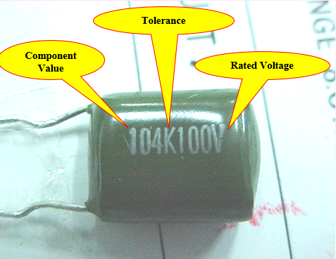
Here is an example of reading a polyester capacitor value. For the capacitor shown in the image, the silkscreen reads 104K. To read its value:
The first two digits: 10 × the third digit 4=10X10000=100000pF=0.1μF
K indicates tolerance: ±10%
100V indicates the rated voltage: 100V

  • Tantalum: Teardrop-shaped, polarized, capacitance and voltage labeled.
  • Unit conversion: 1 F = 10³ mF = 10⁶ μF = 10⁹ nF = 10¹² pF

3. Inductors (L)

How to Read PCB Components Identification?
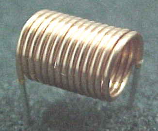
  • Identification: Usually coil-shaped; some use color bands.
  • Reading Parameters:
    • Color-coded inductors: Same method as resistor color codes; units in microhenry (μH).
    • Distinguishing from resistors: Color bands evenly spaced; resistor last band is separated.
  • Special inductors: Used in filters or surge absorbers.

4. Diodes (D) & Transistors (Q/TR)

  • Diodes: Identify polarity; the banded end is the cathode. Includes rectifier diodes and LEDs.
How to Read PCB Components Identification?
  • Transistors: Three leads; check datasheet for pinout.
  • Bridge rectifiers: Multiple diodes in one package for AC-to-DC conversion.

5. Integrated Circuits (ICs)

  • Identification: Usually black with multiple pins.
  • Key point: Identify orientation by notch or dot; pin 1 is lower-left corner, counting counterclockwise.
How to Read PCB Components Identification?

6. Other Components

  • Crystals (X): Metal cans with 2–4 leads, labeled with frequency (e.g., 11.0592 MHz).
How to Read PCB Components Identification?
  • Optocouplers: Like ICs but fewer pins (usually 4–6), used for electrical isolation.
  • Switches/Relays: Recognized by appearance and function.
  • Sockets/Connectors: Various types for connection or expansion.

3. Common Markings and Tolerance Codes

  • Tolerance codes: Letters on silkscreen indicate precision:
    • J = ±5%
    • K = ±10%
    • M = ±20%
    • Capacitors: B = ±0.1pF, C = ±0.25pF, D = ±0.5pF
  • Temperature coefficient codes: E.g., CH, Y5V, indicate capacitance variation with temperature.

In a nutshell, to read PCB components accurately:

  1. Check the PCB symbol: Identify the reference designator (e.g., R1, C2) to know the component type.
  2. Observe component appearance: Determine the general category (resistor, capacitor, diode, etc.).
  3. Read component markings: Decode color bands or printed numbers to get values.
  4. Check polarity: Identify positive/negative terminals for polarized components.
  5. Combine information: Cross-reference all observations to confirm component specifications.

This structured approach ensures accurate and efficient PCB component identification, even for complex or high-density boards.

What Parts of a PCB are Copper?

Simply put, all parts of a PCB responsible for conducting electricity and connecting electronic components are made of copper. Copper acts as the “lifeblood” of a PCB, carrying both electrical signals and power. Here are the main forms and functions of copper on a PCB:

1. Traces

These are the most obvious copper features. Traces act like “highways” or wires on the board, etched into precise patterns on the surface to connect component pins and carry signals and current.

  • Characteristics: The thin lines you see on the PCB are copper traces.

2. Pads

Pads are copper areas used to solder component pins. Whether it’s a copper ring around a through-hole component or a small copper patch under a surface-mount device (SMD), pads ensure a reliable electrical connection between components and traces.

  • Characteristics: Usually appear as slightly larger copper dots, squares, or rings at the end of traces.

3. Vias

To route signals between different layers of a PCB, small holes are drilled and the inner walls are plated with copper, creating a conductive path between layers. These copper walls are called “vias.”

  • Characteristics: Function like “copper bridges” connecting different layers of the PCB.

4. Copper Pour

Large copper areas, often connected to the ground plane (GND), are used to reduce impedance, suppress electromagnetic interference (EMI), and assist with heat dissipation.

  • Characteristics: Appear as large solid or hatched copper areas on the board.

5. Plated Through-Holes

For through-hole components, the inside walls of the holes are plated with copper to ensure the component pins connect to inner or opposite layer circuits.

  • Characteristics: The inner walls of through-hole component holes are copper.

6. Metal Core (Special PCBs)

In high-power or high-performance PCBs, such as metal-core boards used in LED lighting, the entire board core may be a thick copper or aluminum plate with an insulating layer on top, primarily for efficient heat dissipation.

Pls kindly note that the copper on a PCB is usually not exposed. To prevent oxidation and improve solderability, a protective layer is applied over the copper surface, most commonly solder mask. The green color of many PCBs comes from this layer. Silver or gold-colored areas, such as pads, are surface treatments (e.g., tin plating or gold plating), but the underlying material is still copper.

In conclusion, all metallic-looking conductive parts that are not covered by solder mask are fundamentally made of copper.

What are the Functions of PCB Components?

The PCB itself serves as the carrier for all electronic components and circuits. Its core function is to provide mechanical support and electrical connections for electronic components, allowing electrical signals and power to flow according to the design, so that the entire circuit can perform specific functions. Below are common PCB components and their specific functions:

1. Resistor

  • Core Function: Impedes current flow and dissipates energy.
  • Specific Roles:
    • Limiting Current: Controls the amount of current in the circuit to prevent damage to other components.
    • Voltage Division: Distributes voltage across different parts of the circuit, providing suitable operating voltage for other components.
    • Biasing: Establishes a stable operating point for active devices like transistors.
  • Special Resistors:
    • Varistor: Resistance changes with voltage, used for voltage protection and input stabilization, commonly in power supplies.
    • Thermistor: Resistance changes with temperature, used for thermal protection and temperature control.
    • Fuse: A special resistor that quickly blows or increases resistance during abnormal conditions, providing overcurrent protection.

2. Capacitor

  • Core Function: Stores electric charge; “blocks DC, passes AC”.
  • Specific Roles:
    • Filtering: Removes AC ripple from power supplies to smooth DC, or filters specific frequency components in signals.
    • Coupling: Transfers AC signals between circuit stages while blocking DC, preventing interference with DC operating points.
    • Bypass: Provides a low-impedance path for high-frequency noise, bypassing sensitive parts of the circuit.
    • Energy Storage: Charges and discharges rapidly, supplying instantaneous energy to local circuits (e.g., camera flash).
  • Safety Capacitor: Used in power filtering, meeting safety standards to prevent high-voltage surges.

3. Inductor

  • Core Function: Stores magnetic energy; “passes DC, resists AC” (creates reactance for AC).
  • Specific Roles:
    • Filtering: Forms LC filters with capacitors for power and signal filtering.
    • Choking: Blocks high-frequency AC while allowing DC to pass.
    • Resonance: Forms resonant circuits with capacitors for frequency selection and oscillation.
    • Transformer: Two or more coils on a magnetic core for voltage conversion, impedance matching, and electrical isolation.

4. Diode

  • Core Function: Provides unidirectional conduction, allowing current to flow only from anode to cathode.
  • Specific Roles:
    • Rectification: Converts AC to DC (e.g., rectifier diodes, bridge rectifiers).
    • Voltage Regulation: Stabilizes voltage using reverse breakdown characteristics (Zener diodes).
    • Switching: Acts as an electronic switch in digital circuits.
    • Light Emission: Converts electrical energy into light (LEDs).
    • Protection: Prevents reverse current and protects circuits.

5. Transistor

  • Core Function: Current amplification and electronic switching.
  • Specific Roles:
    • Amplification: Amplifies weak electrical signals (voltage, current, or power).
    • Switching: Controls circuit on/off states; fundamental for digital circuits.
    • Control: Used in control circuits, such as voltage regulation and dimming.

6. Integrated Circuit (IC)

  • Core Function: Integrates numerous miniature components—resistors, capacitors, diodes, transistors—into a single chip, forming a complete or partial functional circuit.
  • Specific Roles: Performs complex circuit functions, such as operational amplification, signal processing, microcontrol, logic operations, and power management. It greatly reduces size while improving reliability and performance.

7. Crystal Oscillator

  • Core Function: Generates a highly stable and precise clock frequency using the piezoelectric effect.
  • Specific Roles: Provides a reference clock for microprocessors and digital circuits, ensuring system synchronization and stable operation.

8. Optocoupler

  • Core Function: “Electrical-to-optical-to-electrical” conversion.
  • Specific Roles: Converts an electrical signal at the input to light, then converts it back to an electrical signal at the output. This achieves electrical isolation between input and output and provides excellent anti-interference performance, commonly used for signal isolation and level shifting.

9. Switches and Relays

  • Core Function: Connect, disconnect, or switch circuits.
  • Switch: Manually controls circuit on/off.
  • Relay: Uses a small current (coil) to control a larger current (contacts), enabling automatic control and electrical isolation.

10. Connectors / Sockets

  • Core Function: Provides pluggable connection points.
  • Specific Roles:
    • Connects the PCB to external devices (e.g., power, USB, audio interfaces).
    • Connects PCB to PCB (e.g., board-to-board connectors).
    • Facilitates module installation, replacement, and maintenance.

11. Transformer

  • Core Function: Transforms AC voltage, current, and impedance through electromagnetic induction.
  • Specific Roles:
    • Power Transformer: Steps voltage up or down to the level required by the device.
    • Isolation: Electrically isolates primary and secondary circuits to enhance safety.

In summary, the functions of PCB components work together to achieve these overarching goals:

  • Energy Management: Converts, distributes, and regulates electrical power (e.g., transformers, rectifiers, voltage regulators).
  • Signal Processing: Generates, amplifies, modulates, demodulates, and converts electrical signals (e.g., ICs, transistors).
  • Control and Computation: Performs logic operations and processes data (e.g., microprocessors, logic ICs).
  • Connectivity and Interfaces: Provides reliable connections internally and externally (e.g., connectors, sockets).
  • Protection: Prevents overcurrent, overvoltage, and overheating (e.g., fuses, varistors, thermistors).
  • Support and Mounting: Provides mechanical support for all components (the PCB itself).

What is the PCBA Process?

PCBA stands for Printed Circuit Board Assembly, the process of assembling electronic components onto a bare PCB to create a fully functional board. EBest Circuit (Best Technology) has operated PCB and SMT factories for over 19 years. Our SMT (Surface Mount Technology) production process follows a precise sequence to ensure quality and reliability:

  1. Incoming Materials (BGA/PCB) – All PCBs and components are checked and prepared for production.
  2. Baking – Components and boards are baked to remove moisture and prevent defects during soldering.
  3. Solder Paste Application – Solder paste is applied accurately to pads where components will be mounted.
  4. Printing – Precision printing ensures correct solder paste deposition.
  5. Solder Paste Inspection (SPI) – Verifies solder paste volume and placement for accuracy.
  6. Component Placement (Pick & Place) – Automated machines position components precisely onto the PCB.
  7. Reflow Soldering – Boards pass through a reflow oven, melting the solder paste to secure components.
  8. Tombstone / Tail Cleaning – Removes any excess solder or residue after reflow.
  9. Post-Reflow Inspection – Visual inspection of solder joints and component placement.
  10. Automated Optical Inspection (AOI) – Detects missing, misaligned, or defective components.
  11. X-Ray Inspection – Used for BGA or other hidden solder joints; skipped if no BGA is present.
  12. Secondary Soldering (Post-Solder / Through-Hole Rework) – Completes soldering for components not handled by SMT.
  13. Cleaning – Removes flux and residues to ensure a clean surface.
  14. Programming / Testing – Boards are programmed and tested for functionality.
  15. Conformal Coating – Optional protective coating for moisture and dust resistance.
  16. Gluing / Potting – Adds mechanical support or sealing for sensitive components.
  17. Final Assembly – Complete integration of boards into their final product housing or modules.
  18. Labeling – Applies product labels, serial numbers, and identification marks.
  19. Panel Separation (Depaneling) – Individual boards are separated from the production panel.
  20. Shipping Preparation – Boards are packaged according to customer requirements.
  21. Final Packaging – Options include antistatic bags, tray/knife card, bubble bags, or blister packs for safe shipment.

This workflow ensures that each PCB is highly reliable, fully tested, and ready for integration into final products.

Where to Get PCB Fabrication and PCB Assembly Service?

Choosing the right partner ensures quality, reliability, and right solutions. Our company stands out with five key advantages:

  1. Quality Assurance
    • Advanced equipment: LDI, high-precision drilling, automated VCP plating.
    • Full QC: SPI, AOI, X-ray, flying probe tests, and first-article inspections.
  2. On-Time Delivery
  3. Technical Support
    • Expert engineering support throughout design, production, and after-sales. For example, our free DFM analysis ensures smooth design-to-production workflow.
  4. Customization
    • Flexible tailored solutions in automotive, medical, industrial, aerospace, and telecom sectors.
  5. Customer Experience
    • Online quoting, file transfer, and order tracking systems.
    • Dedicated project managers for clear communication.

In short, EBest Circuit (Best Technology) deliver reliable, high-quality PCB and PCBA services from design to global delivery, giving you best PCBs and optimal solutions.

Above all, understanding the parts of a PCB is essential for anyone involved in electronics. This blog aims to provide a comprehensive overview of the components of a PCB and their Functions. If you have any procurement needs for parts of a PCB, PCB manufacturing, or SMT needs, just feel free to reach out to sales@bestpcbs.com for our expert help.

FAQs

1. What are the four basic components of a circuit?

  • The four fundamental components in most electronic circuits are:
  1. Resistors – Limit current flow and divide voltage.
  2. Capacitors – Store and release energy, filter signals, and block DC while passing AC.
  3. Inductors – Store magnetic energy and resist changes in current; often used in filters and transformers.
  4. Power Source – Provides the necessary electrical energy, such as a battery or power supply.

Together, these components control, store, and direct electrical energy to perform specific circuit functions.

2. What is the general structure of a PCB?

  • A PCB (Printed Circuit Board) is a flat board that mechanically supports and electrically connects electronic components. Its general structure includes:
  • Substrate (Base Material) – Provides mechanical support, commonly made of FR-4, aluminum, or flexible materials.
  • Copper Traces – Conductive paths that connect components.
  • Solder Mask – Protective layer that prevents short circuits and oxidation, typically green.
  • Silkscreen – Printed labels for component identification and orientation.
  • Components – Mounted on the board via surface mount or through-hole technology.

This layered structure allows a compact, reliable, and organized circuit layout.

3. What are the PCB layers?

  • PCBs can have multiple layers depending on circuit complexity. The main layers include:
  1. Top Layer – Usually holds most surface-mount components and signal traces.
  2. Inner Layers – Used for routing signals, power, and ground planes in multi-layer boards.
  3. Bottom Layer – May carry components and traces on the opposite side.
  4. Substrate Layer – The insulating base that separates conductive layers.
  5. Solder Mask & Silkscreen – Protective and labeling layers on the top and bottom surfaces.

Multi-layer PCBs allow higher component density and improved electrical performance, such as reduced EMI and better signal integrity.

You may also like