Stacked microvias connect successive HDI layers by placing filled microvias directly above one another. They save routing space under dense packages, but add interfaces that must survive fabrication, assembly reflow and service. Use them when a simpler fanout cannot meet the routing requirement—not simply because the CAD tool lets you stack vias.
Start with three decisions: which layers actually need connecting, whether lateral staggering fits, and what evidence qualifies that exact construction. A small hole that passes room-temperature continuity is not, by itself, proof of a reliable stacked interconnect.
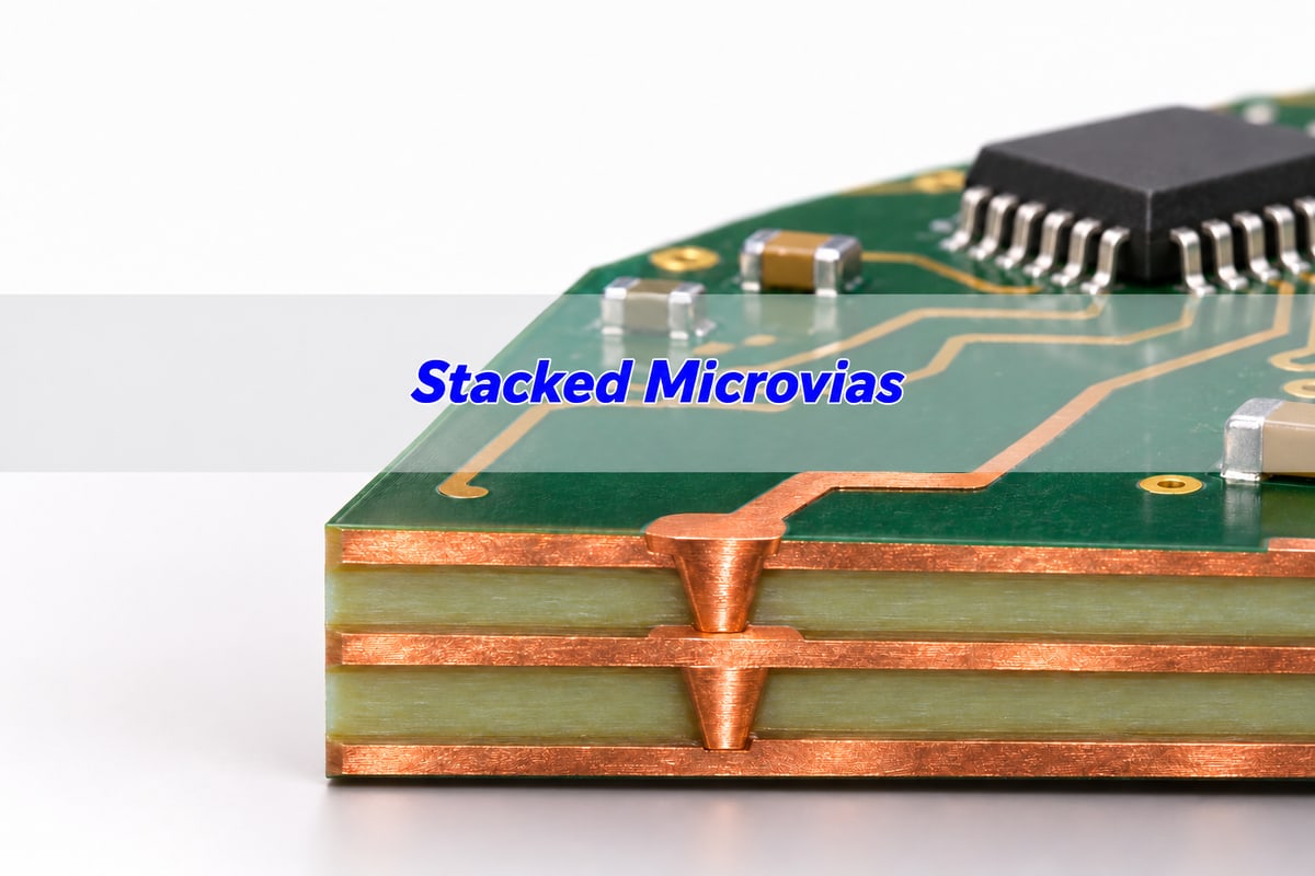
Stacked Microvias: How the Connection Works
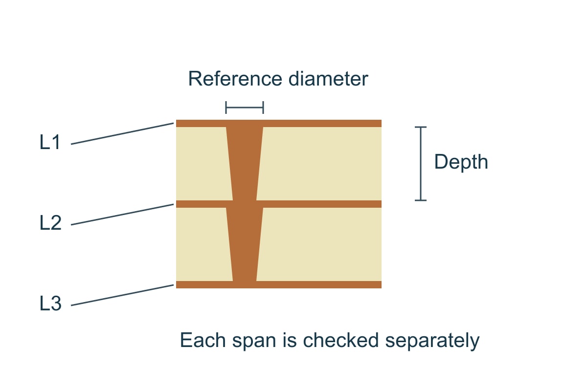
Each microvia connects a shallow layer pair. In a two-high stack, one connects L1 to L2 and a second connects L2 to L3. Their connection is through the intermediate copper landing structure, not through a single long laser hole. Sequential processing creates the lower interconnect before the next dielectric and via are added.
That distinction matters in a fabrication drawing. “L1–L3 connection” could describe different constructions. Identify the individual spans, copper filling, cap or landing requirements and permitted stack locations. Otherwise, electrical connectivity may match while the actual manufacturing structure does not.
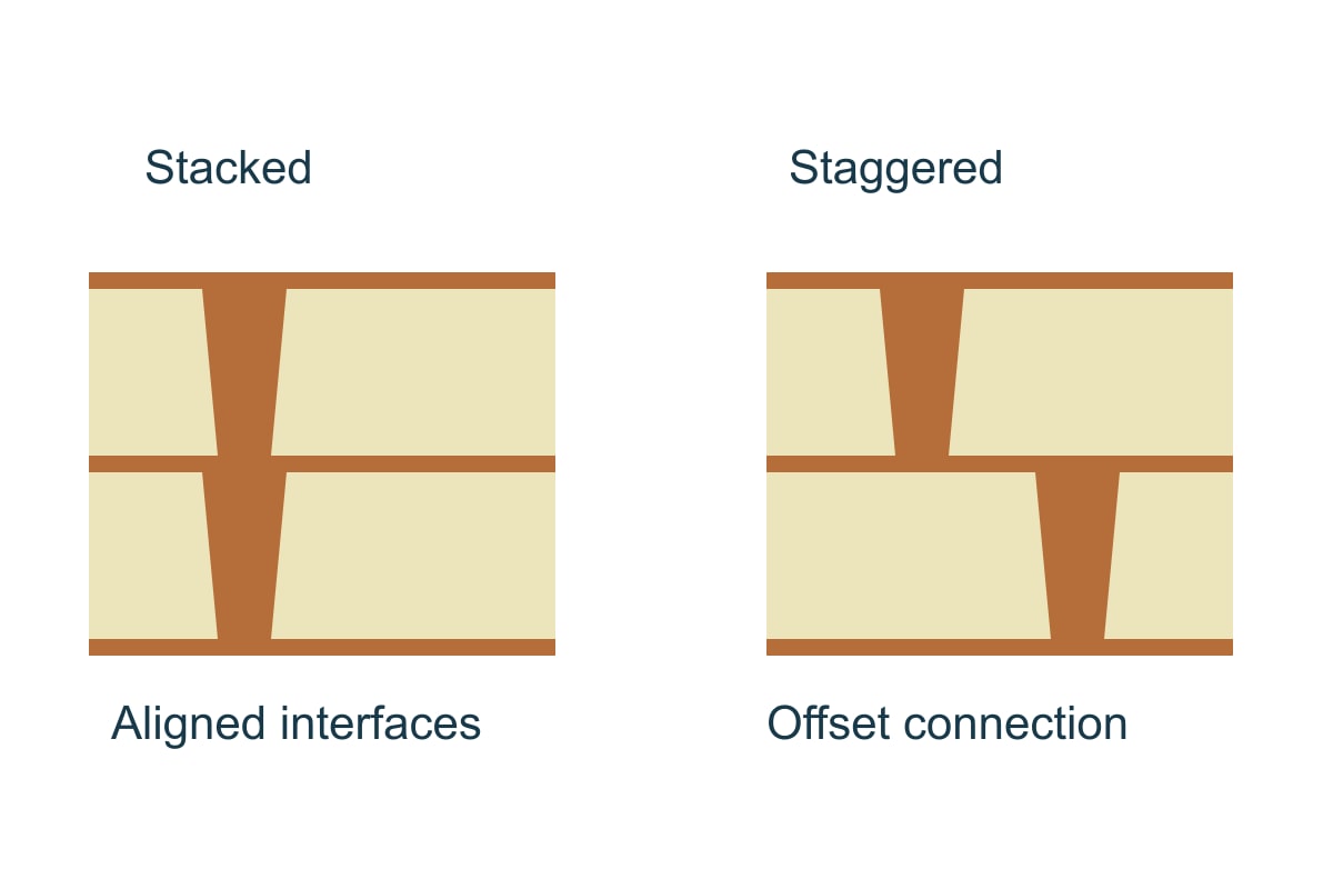
Stacked vs Staggered Microvias: Which Layout Fits?
Stacked microvias use less lateral space; staggered microvias move successive holes apart and connect them through an intermediate conductor. The better choice depends on escape space and qualified manufacturing—not a universal ranking of via types.
| Construction | What it gives you | What you must check |
| Stacked | Compact vertical escape through successive buildup layers | Filled target structure, stacked interfaces and thermal qualification for the exact stack |
| Staggered | An offset connection between layer-pair vias | Room for both capture lands and the connecting copper; no unintended hole intrusion |
| Single-level microvia | One shallow layer transition with fewer stacked interfaces | Whether one added routing layer actually completes the fanout |
| Through via | A full-board connection without sequentially stacked microvias | Drill/pad area, unused barrel and the layers it blocks |
Try the lowest-complexity construction that completes the escape. If staggering fits without unacceptable trace congestion, it deserves a layout trial. If it does not fit, stacking may be justified, but the saved area must be weighed against additional fabrication and qualification work. NCAB’s HDI guidance specifically highlights problems with unclear via requirements and overlapping staggered structures.
Microvia Aspect Ratio: Calculate Each Layer Span
Calculate aspect ratio for each individual microvia: AR = via depth ÷ agreed reference diameter. State which diameter the fabricator uses; a tapered laser hole has different entrance and target dimensions. Do not compare ratios calculated with different definitions.
For a hypothetical 60 µm-deep microvia and a 100 µm reference diameter, AR = 60/100 = 0.60. If dielectric depth becomes 100 µm while that diameter stays unchanged, AR becomes 1.00. The second structure is harder to process consistently; neither number alone establishes approval.
A two-high stack of 60 µm spans does not turn each microvia into a 120 µm-deep hole. Review each span and then review the complete stacked structure separately. Obtain approved minimum target size, capture land, registration allowance and fill criteria from the intended fabricator before finishing the escape.
Copper-Filled Microvias: Why the Target Surface Matters
A via stacked over another microvia needs a suitable conductive landing structure. Copper filling and the finished target surface serve an electrical and mechanical purpose; resin filling alone is not the same construction. “Filled via” is therefore an incomplete purchase requirement.
Specify the fill material and whether the location also serves as a component solder pad. A resin-filled, copper-capped through via and a copper-filled microvia are different structures, even if their top pads look similar. Do not substitute one based only on a flat surface or a generic via-protection description.
Ask how target preparation, plating and planarization are controlled. A visually flat pad cannot reveal every buried interface defect. Review representative sections together with electrically monitored thermal evidence rather than treating either as a complete substitute for the other.
Stacked Microvias Reliability: What Can Fail?
The critical concern is an interconnection that opens under thermal stress, even though it passed an earlier electrical test. Temperature changes create differential expansion between dielectric and copper; weak interfaces can separate when stressed and reconnect after cooling.
If a board works before assembly but fails after reflow, first establish when the resistance changes. Compare monitored behavior during a representative thermal exposure with room-temperature measurements, and use failure analysis to locate the discontinuity. A good room-temperature reading after the event does not exclude a transient open.
Changing only to a higher-Tg laminate is not a complete corrective action. Material expansion, buildup thickness, via geometry, target quality and process history all remain relevant. Treat a change in material, via stack height or fabricator as a qualification-impacting change, not a clerical substitution.
IPC Stacked Microvias: Specify the Right Evidence
Use IPC documents according to their purpose. IPC-2226 addresses HDI design; IPC-6012 addresses rigid-board qualification and performance; IPC-A-600 provides bare-board acceptability guidance. They are not interchangeable labels for “reliable.”
The public IPC standards overview pairs IPC-6012F with IPC-A-600K. Your purchase drawing must state the contractually applicable revision, performance class and any customer requirements; this guide does not reproduce paywalled clauses or invent a universal microvia pass limit. Ask the supplier to identify the applicable microvia structural-integrity and thermal-stress provisions in that agreed edition.
Würth Elektronik’s published HDI reliability presentation illustrates why via type and test conditions must be considered together. Its example recommendations and study results are not automatic acceptance limits for another factory or your product.
HDI PCB Stackup: Work Through One Escape Decision
Consider an illustrative dense controller board that must reach L3 from a top-side BGA. First check whether L2 routing can finish the escape. If not, compare a two-high stack with two staggered layer-pair microvias in the same actual fanout region.
| Planning input | Worked example | Decision or next action |
| L1–L2 depth / diameter | 60 µm / 100 µm = 0.60 AR | Confirm the fabricator uses the same diameter definition |
| L2–L3 depth / diameter | 60 µm / 100 µm = 0.60 AR | Approve this second span independently |
| Staggered land diameter and center offset | 250 µm land + 200 µm offset = 450 µm total envelope | Compare 450 µm with available escape space, before adding other clearances |
| Stacked alternative | 250 µm nominal land envelope in this simplified plan view | Check registration, routing and qualified stack construction; compact does not mean approved |
| Release evidence | Drawing revision + representative coupon + thermal test report | Hold release if the tested structure differs from the production structure |
These are hypothetical layout inputs, not factory capability limits. The 450 µm envelope is simply the distance from one outer land edge to the other for equal lands along the offset direction. It excludes adjacent-trace clearance and registration margins. If the corridor is only 400 µm wide, this trial staggered geometry does not fit; you must change the geometry, layer strategy or construction—not delete the missing clearance.
Stacked Microvias Applications: Match the Construction to the Job
Compact modules and wearables: stacking can free escape area when package density dominates. Check actual routing completion, land registration and assembly-pad requirements. Success means all necessary nets escape within approved rules and the built structure survives the agreed assembly profile; smaller board area alone is not success.
Network and high-speed boards: shallow interconnects can avoid a long unused via barrel, but a stacked connection is still an electromagnetic discontinuity. Review the signal transition, reference-plane path and return vias against the interface budget. Use suitable field analysis or measurements on representative transitions; do not infer insertion loss from “HDI.”
Industrial or other long-service products: thermal cycling and rework exposure can outweigh a small area saving. Compare staggered or simpler constructions early. Qualification must represent the intended material, board build and relevant service stresses; a consumer-board success story does not establish the same lifetime for another application.
Microvia Qualification Checklist: Read the Report Before Release
Use the following as a release tool. For every production stack, record the layer spans, fill and target structure, material and thicknesses, coupon correspondence, thermal exposure, electrical monitoring method and acceptance rule. Then mark each item supported, missing or not applicable.
Example: if your board has a two-high L1–L3 stack, but the supplied report covers only L1–L2 single microvias, mark “structure correspondence: missing” and request representative evidence. Do not record “pass” just because both documents say microvia.
Check how resistance was monitored, when readings were taken, and whether the report identifies transient events. Cross-sections help identify structure and localized defects; they sample specific locations. Neither a single attractive section nor continuity at the end of testing establishes every relevant failure mode.
For a closer look at the measurement issue, see our microvia reflow resistance-trace guide. Tie the final release to documented evidence and agreed acceptance—not to an unsupported maximum stack count.
Stacked Microvias FAQs
Are two stacked microvias automatically safe?
No. Stack count does not establish process quality or service suitability. Review the exact material, layer spans, filled target construction and qualification evidence. A qualified two-high structure from one process is not automatic approval for a changed process.
Can a stacked microvia land on a buried via?
That compound structure needs separate evaluation. The buried-via fill, cap, dimensions and interaction with the stacked microvias affect the construction. Do not assume evidence for a microvia stack on a solid internal land covers a stack over a filled buried via.
Does via-in-pad always require stacked microvias?
No. Via-in-pad describes the via location relative to a component pad. A single-level microvia can be via-in-pad without being stacked. Specify pad requirements and layer connectivity separately.
Can I use one CAD via definition for the whole stack?
Only if the output unambiguously communicates every layer-pair construction and matches the approved fabrication drawing. A net connection or a single drill symbol cannot replace the buildup and via-span definition.
Why can the board pass before assembly and fail afterward?
Reflow can expose an interconnect weakness that was not open during the original electrical test. Preserve the affected boards and thermal history. Compare monitored resistance through representative thermal exposure and use failure analysis before assigning the cause.
Does a thicker copper fill fix every reliability problem?
No. More copper does not remove a weak interface, incorrect target preparation or an unqualified geometry. A process or geometry change needs evidence showing which failure mechanism it addresses.
Are staggered microvias always cheaper?
No. Cost depends on sequential buildup cycles, panel utilization, fill, registration and yield requirements. Compare quotations for constructions that meet the same routing and qualification needs; do not apply a generic percentage discount.
What should I send before asking for an HDI quotation?
Send fabrication data, the stackup, via-span and fill definitions, quantities, assembly thermal exposure and required acceptance criteria. Include qualification requirements at quotation stage so the quoted route and release evidence describe the same product.
Technical References
- NCAB: HDI PCB technical specification and via-construction considerations.
- Würth Elektronik: HDI miniaturization, cost and reliability presentation; via-type and IST sections.
- IPC standards overview: design, performance and acceptability documents have different purposes.
Custom HDI PCBs with Engineering Review
Need a dense board that can be manufactured—not just routed? Send your HDI stackup and fabrication files to EBest Circuit. Our PCB manufacturing and PCBA services let you discuss the bare-board construction and assembly requirements together, so the quotation starts with the product you actually need.
Include via spans, fill requirements, quantities and reliability requirements. Ask us to confirm the supported construction and quotation scope before you freeze the design. Request your custom HDI PCB review and quote at sales@bestpcbs.com.
You may also like





Tags: HDI PCB, Microvia Reliability, pcb stackup, Stacked Microvias