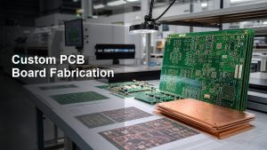
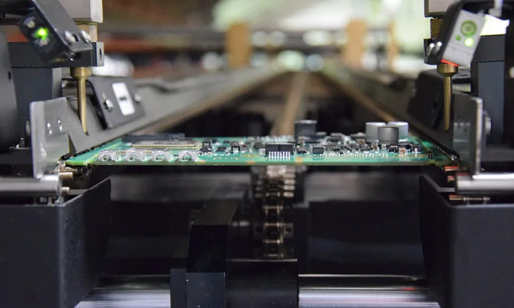
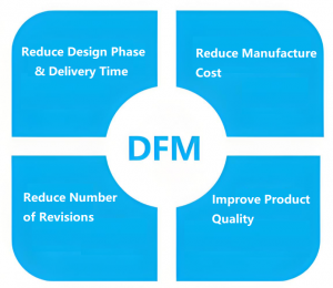
A custom through-hole PCB should be designed from the component leads outward: confirm the real lead dimensions, define finished holes and pads with the fabricator, reserve assembly access, and send complete fabrication and assembly files. The board is only ready for quotation when the manufacturer can identify every drilled hole, plated feature, component orientation, soldering method, inspection requirement, and acceptable substitution without guessing.
This guide focuses on the decisions that connect a through-hole schematic to a manufacturable board and an accurate RFQ. It complements our broader explanation of through-hole circuit board construction, plating, and assembly.
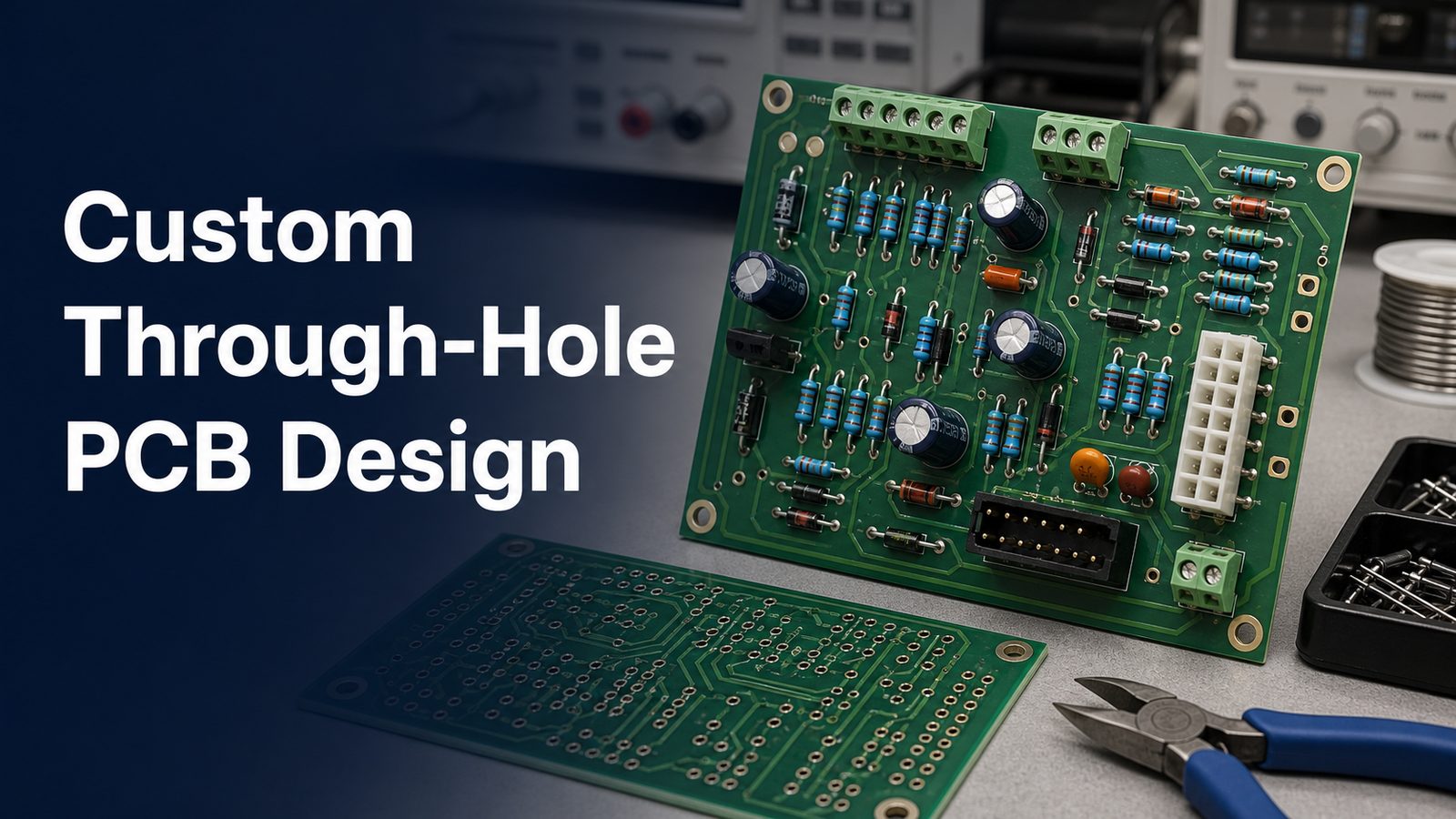
What Is a Custom Through-Hole PCB?
A custom through-hole PCB is a printed circuit board whose plated holes, pads, component footprints, mechanical outline, and assembly method are designed for a specific set of leaded components and operating constraints.
Through-hole technology (THT) places component leads through drilled holes and solders them on the opposite side. It is often selected for connectors, transformers, relays, terminal blocks, large electrolytic capacitors, switches, or other parts that need mechanical retention, serviceability, or compatibility with an existing design. A board can be entirely through-hole or use mixed technology, with SMT parts on one or both sides and selected THT parts added later.
“Custom” does not simply mean a nonstandard outline. The drill table, lead pattern, component height, copper connection, solder access, fixture needs, panel direction, and inspection criteria may all change the manufacturing route.
When Does Through-Hole Technology Make Sense?
Through-hole technology makes sense when component availability, mechanical loading, manual service, high-mass parts, or legacy compatibility matters more than maximum placement density.
| Design condition | Why THT may help | What to verify |
| Frequently mated connector | Leads can transfer mechanical load through the board | Connector retention, board support, pad geometry, enclosure load |
| Large transformer, relay, or capacitor | Lead insertion provides stable placement before soldering | Mass, vibration, creepage, keepouts, adhesive or mechanical support |
| Prototype or field-service design | Leaded parts may be easier to probe and replace manually | Expected rework cycles and pad durability |
| Legacy product | Existing BOM and mechanical interfaces can be retained | Lifecycle, alternates, obsolete footprints, documentation quality |
| Mixed SMT and THT assembly | Dense SMT circuitry can coexist with mechanically loaded THT parts | Process order, bottom-side clearances, soldering method, fixture access |
THT is not automatically more reliable in every design. Reliability depends on the complete interconnect system: component construction, hole and pad design, laminate, copper plating, solder process, mechanical support, cleanliness, inspection, and operating environment.
How Should You Build a Through-Hole Footprint?
A through-hole footprint should be built from the current component drawing, not from a nominal package name or an unverified library symbol.
Check the lead count, pitch, lead cross-section, body size, standoff, insertion side, pin-one convention, polarization, mating direction, tolerance, and any locating or retention features. For rectangular or tab-shaped leads, the diagonal and orientation may control the required hole more than the nominal width.
- Record the component manufacturer and exact orderable part number.
- Use the latest mechanical drawing and note its revision.
- Separate electrical leads from tooling, locating, or non-plated mounting holes.
- Show polarity and pin-one marks on assembly documentation and silkscreen where space permits.
- Check the courtyard against neighboring parts, insertion tools, test probes, and enclosure walls.
- Confirm whether the part must sit flush, use a controlled standoff, or receive extra mechanical support.
A library footprint can be a starting point, but the released footprint should be traceable to a controlled component drawing. This is especially important for connectors and electromechanical parts whose similar product names may hide different pin spacing or retention posts.
How Do You Specify Finished Holes and Pads?
Specify the required finished-hole size and let the PCB fabricator account for its validated drilling and plating process; do not assume the drill tool equals the finished plated hole.
The required clearance depends on the maximum lead envelope, lead shape, component tolerance, insertion method, board fabrication tolerance, plating allowance, and assembly process. The correct value is therefore a design decision to confirm with both the component drawing and the selected manufacturer rather than a universal number copied from another board.
| Feature | Design input | Manufacturing question |
| Finished plated hole | Maximum lead envelope plus validated insertion clearance | What finished-hole tolerance can be held for this stackup and quantity? |
| Pad and annular ring | Current, mechanical load, breakout risk, routing space | What minimum retained annular ring is supported after registration tolerances? |
| Thermal connection | Required current, heat flow, solderability | Will the copper connection cause difficult heating or insufficient solder fill? |
| Non-plated hole | Fastener, locating post, tooling, isolation | Is it clearly separated from plated drill data and copper clearances? |
| Slot or unusual lead | Tab dimensions and orientation | Is the slot plated, routable, and compatible with the assembly process? |
Large copper planes around a THT pad can draw heat away during soldering. Thermal-relief geometry may improve solderability, but it must still meet current and mechanical requirements. Ask the fabricator and assembler to review the actual copper connection instead of applying one default rule to power terminals, signal pins, and structural leads.
What Layout Details Affect Through-Hole Assembly?
Through-hole layout must reserve physical access for insertion, lead trimming, soldering, inspection, rework, and any fixture that supports the board.
Keep polarized parts consistently oriented where practical. Leave enough space to read assembly markings and to reach solder joints without damaging adjacent components. Tall or heavy parts may need spacing from board edges and vibration-sensitive areas. Connectors must be checked in the mated condition, not just as an isolated footprint.
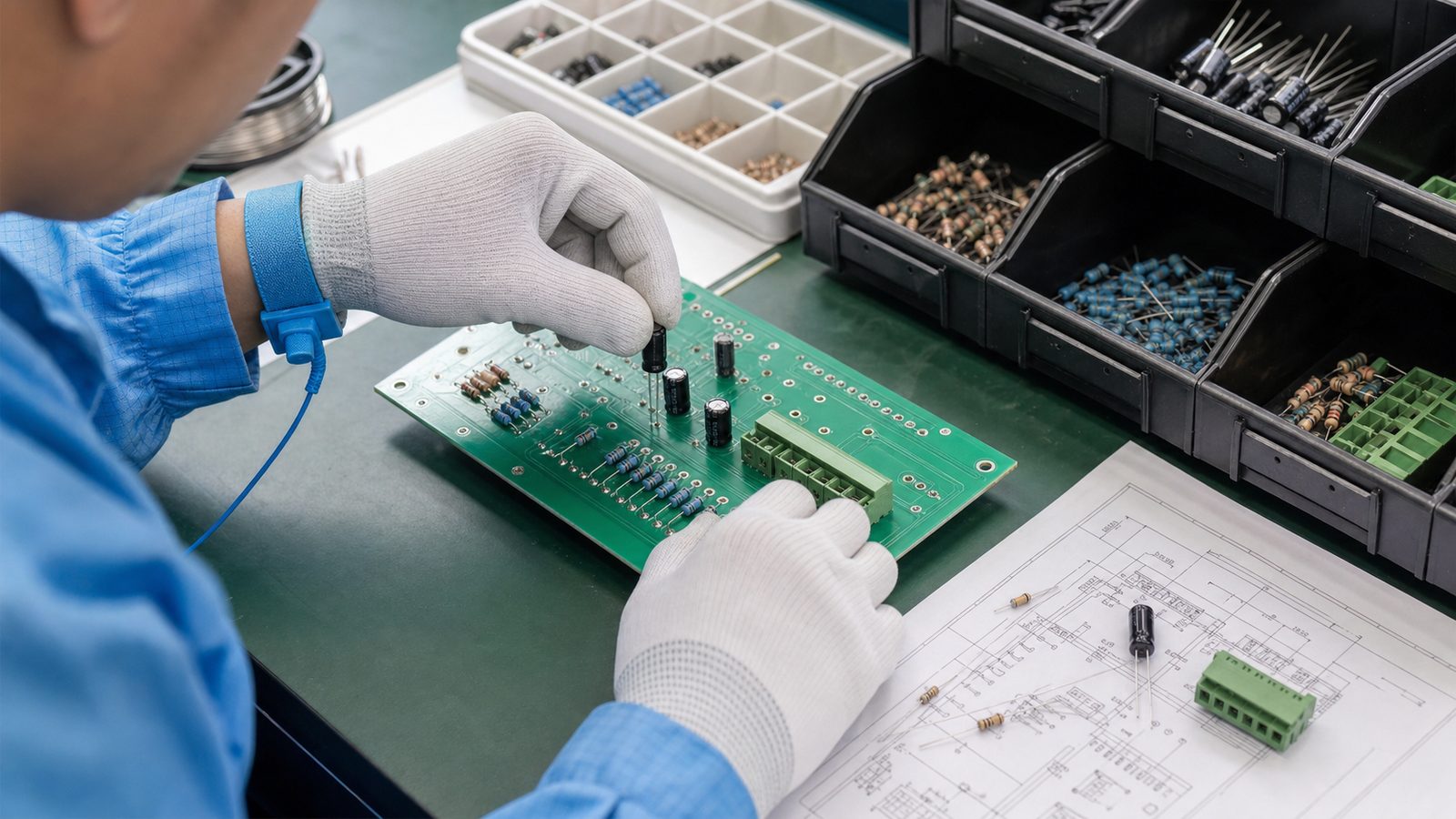
For mixed-technology boards, review the entire process sequence. Bottom-side SMT components can interfere with wave pallets or selective-solder nozzles. A component that is easy to place by hand may still block automated soldering or inspection. If prototype and production quantities will use different soldering methods, design for both routes or document the intended change.
Which Soldering Method Should You Plan For?
Choose hand soldering, wave soldering, or selective soldering according to volume, component distribution, thermal mass, bottom-side obstructions, repeatability needs, and fixture cost.
- Hand soldering suits prototypes, repairs, low volumes, and joints that need individual access, but workmanship consistency and cycle time require control.
- Wave soldering can process many accessible THT joints efficiently when the underside layout, component orientation, masking, and pallet strategy support the process.
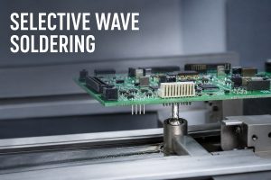
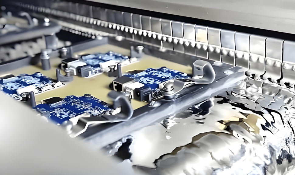
- Selective soldering targets defined joints or regions and can suit mixed-technology boards where a full solder wave would contact protected areas.
The short comparison below shows the practical difference between wave and selective soldering. It belongs here because the decision directly changes layout clearances, fixtures, process time, and RFQ assumptions.
When the assembly route is not yet fixed, ask for a DFM review from the intended through-hole assembly service before freezing the bottom-side layout.
What Quality Checks Matter for a Custom Through-Hole PCB?
Quality checks should verify the bare board, component installation, solder joints, cleanliness, electrical function, and any mechanical load that the assembly must carry.
Bare-board review can include drill and plating conformity, continuity and isolation testing, hole position, annular ring, board dimensions, and surface condition. Assembly inspection should check correct components, orientation, seating, lead condition, solder coverage, bridges, void-related concerns where visible or otherwise inspectable, flux residues, and damage from handling or rework.

Do not write “IPC Class 2” or “Class 3” on an RFQ without identifying the applicable acceptance document, revision, product requirements, exceptions, and evidence expected from the supplier. If a connector carries repeated mechanical load, a functional or mechanical test may be more informative than appearance alone.
What Causes Common Through-Hole PCB Problems?
Most through-hole problems can be traced to an incorrect footprint, poorly defined hole or copper connection, unstable component retention, unsuitable solder access, uncontrolled thermal demand, or incomplete work instructions.
| Observed problem | Possible design or process cause | Review action |
| Part will not insert consistently | Lead envelope, hole tolerance, pitch, slot orientation, or bent leads | Compare the physical part, drawing, footprint, and finished-hole data |
| Weak or inconsistent solder joint | Thermal imbalance, contamination, access, process window, or geometry | Review copper connections, materials, cleaning, profile, and acceptance criteria |
| Component lifts or tilts | Poor retention, uneven leads, fixture limits, or solder forces | Define seating, lead forming, retention, and fixture method |
| Pad or barrel damage during rework | Excess heat, force, dwell time, or repeated repair cycles | Define approved rework method and evaluate repairability during design |
| Connector fails mechanically | Board flex, enclosure load, inadequate support, or incorrect footprint | Review the complete mated mechanical system and load path |
What Files Are Needed for an Accurate RFQ?
An accurate RFQ needs enough controlled data for fabrication, procurement, assembly, inspection, and acceptance without relying on assumptions.
- Gerber or ODB++ fabrication data with a clearly identified revision.
- NC drill files that distinguish plated and non-plated holes, plus slot definitions.
- Fabrication drawing with board outline, stackup expectations, material, copper, finish, thickness, tolerances, and notes.
- BOM with manufacturer part numbers, approved alternates, quantities, and do-not-fit status.
- Assembly drawings for each populated side, including polarity and reference designators.
- Centroid data for SMT portions of mixed-technology boards.
- Special instructions for lead forming, insertion depth, standoff, clinching, adhesive, hardware, conformal coating, cleaning, or masking.
- Inspection and test requirements, including fixtures, firmware, test limits, and acceptance records.
- Prototype and forecast quantities, packaging needs, and any component consignment plan.
For early builds, a prototype PCB assembly run can confirm footprint fit, insertion access, soldering behavior, and test coverage before production tooling is finalized. If schedule is critical, compare the files and approvals needed for a quick-turn PCB assembly route rather than asking only for the shortest calendar lead time.
Custom Through-Hole PCB Pre-Release Checklist
A design is ready to release when the electrical, mechanical, fabrication, assembly, and inspection data agree with one another.
- Match every footprint to the current component drawing and exact orderable part.
- Confirm maximum lead dimensions, pitch, orientation, and retention features.
- Define finished plated holes, non-plated holes, slots, pads, and copper connections.
- Check component body, height, mating, tool, probe, enclosure, and rework clearances.
- Select the intended soldering route and review bottom-side access and fixture needs.
- Review heavy parts, connectors, board flex, vibration, and mechanical support.
- Align fabrication drawing, BOM, assembly drawing, drill data, and revision identifiers.
- Define inspection, electrical test, functional test, cleanliness, and acceptance evidence.
- Run DFM and assembly review before ordering production quantities.
- Validate the prototype with the actual enclosure, cables, mating connectors, firmware, and test fixture.
Frequently Asked Questions
Is a through-hole PCB the same as a plated-through-hole PCB?
Not necessarily. “Through-hole PCB” often describes a board assembled with leaded components, while “plated through-hole” describes a hole with conductive plating connecting pads or copper layers. A board may contain plated through-holes as component holes or vias even when most components are surface mounted.
Can a custom board use both SMT and through-hole components?
Yes. Mixed-technology assemblies are common when dense SMT circuitry must coexist with connectors, relays, transformers, or other leaded parts. The layout must account for process order, bottom-side SMT parts, wave pallets or selective-solder access, inspection, and rework.
How much clearance should a lead have inside a finished hole?
There is no single clearance that fits every component and process. Use the maximum lead envelope, lead shape, insertion method, component tolerance, finished-hole tolerance, plating process, and assembly capability. Confirm the final value with the component drawing and manufacturer before release.
Should the PCB drawing specify drill size or finished-hole size?
The design documentation should clearly communicate the required finished feature and tolerance. The fabricator normally selects a process drill that accounts for plating and its controlled manufacturing route. Ambiguous drill notes can lead to incorrect assumptions, so align the drill files and fabrication drawing.
Are thermal reliefs always required on through-hole pads?
No. Thermal reliefs can improve solderability when a pad connects to a large copper area, but high-current, heat-transfer, or mechanical requirements may call for a different connection. Review electrical and thermal needs together with the solder process.
When is selective soldering better than wave soldering?
Selective soldering is useful when only defined THT joints can contact solder or when bottom-side SMT parts and sensitive areas prevent full wave exposure. Wave soldering can be efficient for layouts designed around broader underside access. Volume, fixture cost, spacing, and thermal demand also affect the choice.
What should be included in a through-hole assembly drawing?
Show component locations, reference designators, insertion side, polarity, pin one, orientation, do-not-fit parts, special seating or standoff requirements, hardware, lead forming, and revision. Add separate controlled instructions when soldering, masking, cleaning, coating, or test requirements need more detail.
How can connector solder joints be protected from mechanical stress?
Design the load path across the connector, board, mounting hardware, enclosure, and cable. Board supports, retention features, fasteners, strain relief, adequate pad and hole design, and controlled mating forces may all matter. Do not expect solder joints alone to absorb repeated external load.
What should be tested on a first prototype?
Verify component fit, polarity, insertion and solder access, electrical continuity, programmed function, connector mating, enclosure fit, temperature behavior, mechanical loads, test-point access, and rework feasibility. Record every change against the controlled design revision before production release.
How do I reduce quotation delays?
Send synchronized fabrication data, drill files, BOM, assembly drawings, test requirements, quantities, and revision identifiers. Flag alternate parts and special processes clearly. A concise question list for unresolved items is better than leaving the supplier to infer missing requirements.
Final Design Decision
A custom through-hole PCB succeeds when the component drawing, finished-hole definition, copper connection, assembly access, soldering route, inspection plan, and RFQ package describe the same product. Resolve those interfaces before production, not during component insertion.
If you are preparing a through-hole or mixed-technology PCB for prototype or production, send the engineering files, BOM, expected quantities, soldering constraints, and test requirements to sales@bestpcbs.com for DFM review and quotation.