PCB manufacturing PCB manufacturing
Home > Blog

Circuit Board Ground Plane

Circuit Board Ground Plane: Layout Rules and Return Paths
Wednesday, September 2nd, 2026

A circuit board ground plane is a broad copper region connected to a PCB’s ground net. It provides a voltage reference and a path for returning current. Its effectiveness depends on continuity, distance from the signal layer and the connections between layers, not simply how much copper fills the screen. A layout can pass a continuity test yet still force fast return currents through a noisy detour.
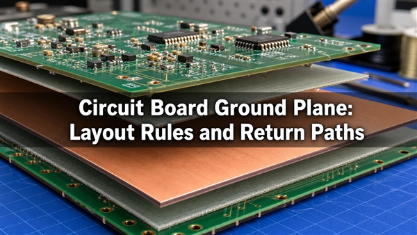
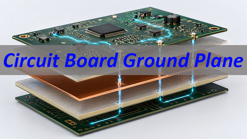
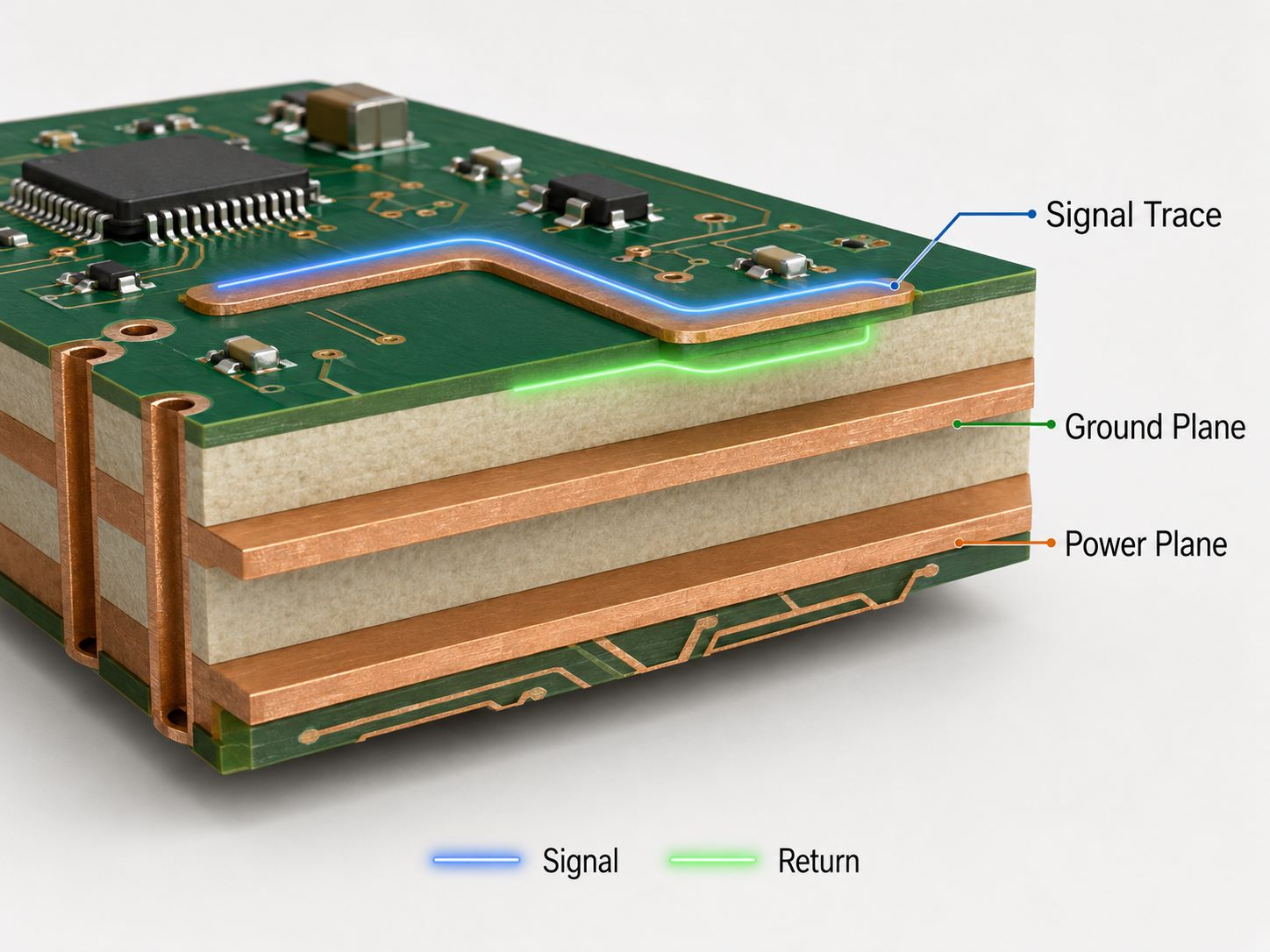
Circuit board ground plane illustrated as a continuous copper layer beneath insulated signal routing

What Is a Ground Plane?

A ground plane in PCB design is the physical copper conductor assigned to the reference net, usually named GND. In PCB terminology, a GND plane or grounding plane, sometimes written groundplane, can occupy most of an outer layer or a dedicated internal ground layer. It is not automatically connected to earth: a battery-powered circuit can have a local ground reference without an earth connection.

For the question “what is a ground plane PCB?”, the distinction is straightforward: the PCB is the complete board, while its ground plane is one part of the copper structure. Schematic ground symbols specify connectivity; the manufactured copper determines the impedance of that connection.

Ground planes are also different from chassis bonds and protective-earth conductors. Those connections address enclosure, fault-current and system-level requirements. A common net name does not make their functions interchangeable.

How Does a Ground Plane Work?

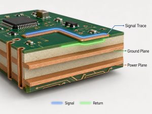
A ground plane completes the current loop between a source and its load. At low frequency, resistance strongly influences current distribution; with fast signal transitions, inductance and electromagnetic coupling become important. The high-frequency portion of the return current tends to concentrate on the nearby reference plane beneath the signal path.

The return is a distributed current, not a narrow physical track etched into the plane. A continuous reference lets that distribution follow the signal. A slot, a chain of clearance holes or a long narrow copper neck can force it elsewhere, increasing loop area and changing the local transmission-line geometry.

For example, routing a clock over an uninterrupted ground region and routing the same clock over a connector cutout are not equivalent, even if both endpoints connect to GND. Trace length alone will miss that difference. Circuit board grounding must be evaluated as a complete outgoing-and-returning path.
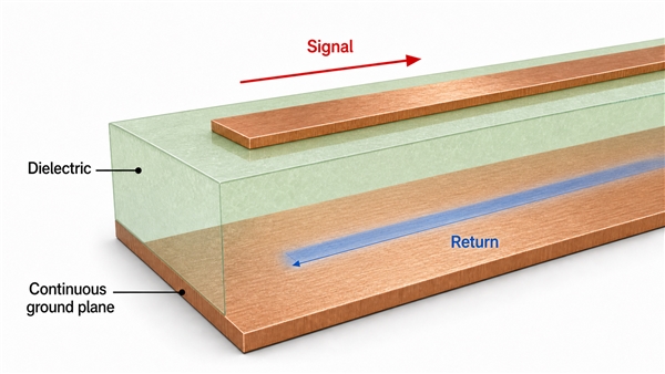
Conceptual signal and opposing high-frequency return directions on separate layers, not to scale

Which PCB Ground Plane Rules Matter Most?

The most useful PCB ground plane rules protect a continuous reference under critical routes and control where noisy currents travel. A large copper percentage is not a substitute for these checks.

  • Choose the stack-up before routing. Identify the reference conductor for each signal layer, including the layer after every transition.
  • Keep critical routes over continuous copper. Check slots, antipads, plane edges and narrow connections, not only obvious split lines.
  • Place by current flow. Keep switching loops and digital interfaces away from low-level analog input paths.
  • Provide local return transitions. Connect same-net ground references near signal-layer changes where the return must change planes.
  • Preserve clearances. Copper fill must not violate electrical spacing, board-edge or isolation requirements.
  • Inspect the filled result. Refill copper after layout changes and review the manufacturing output, not just the polygon boundary.

PCB ground plane design should also account for edge rate. A low clock frequency does not mean its digital edges are slow. Plane spacing, trace geometry and the device’s transition times together determine whether a seemingly short connection needs transmission-line treatment.

How Should a 2 Layer PCB Ground Plane Be Arranged?

A 2 layer PCB ground plane is usually easiest to preserve when most components and signal routing remain on one side and the other side stays predominantly ground. Every trace inserted into that ground side consumes some of the available return path.

On a 2 layer circuit board, a short crossover may be manageable, but a row of parallel bottom-side traces can divide the copper into long strips. Move components or reroute the upper layer before accepting a ground region connected only by a thin neck. Inspect the copper underneath each fast or sensitive route from source to load.

A 2 layer PCB board is not automatically unsuitable for fast signals, but it provides fewer routing options for maintaining a close, continuous reference. A thick two-layer dielectric can also make practical controlled-impedance routing more difficult. Compare the proposed geometry with a manufacturable four-layer stack before locking the board thickness.

We manufacture FR4 printed circuit boards for these constructions. Layer count, dielectric spacing and copper thickness should be considered together; adding a copper pour after routing cannot correct every return-path problem.

What Changes with a 4 Layer PCB Ground Plane?

A 4 layer PCB ground plane can provide a dedicated internal reference that routing does not repeatedly interrupt. The benefit comes from the actual layer arrangement, not the number four itself.

Illustrative stack-up Useful feature Design limitation
Signal / dielectric / GND Simple two-layer construction Ground-side routing and large dielectric spacing can constrain performance
Signal / GND / power / signal Dedicated ground and power distribution Bottom routing often references the power plane; splits and reference transitions need attention
Signal-power routing / GND / GND / signal-power routing Both outside signal layers can have adjacent ground references Power must be distributed in suitable traces or pours; current capacity still needs checking

PCB power and ground planes serve different nets. A PCB power plane can act as an AC reference in a suitable design, but return transfer to ground depends on the power-distribution network, including decoupling and plane coupling. Do not assume a signal via automatically provides that transfer.

For multilayer circuit board planes, specify the copper order and actual dielectric thicknesses. Two boards with the same total thickness can have very different trace-to-reference spacing. The drawing below illustrates two possible arrangements, not a production stack-up specification.
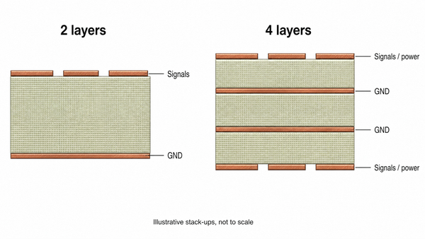
Two-layer and four-layer examples showing signal conductors separated from continuous ground copper by dielectric

Should a PCB Ground Plane Be on the Top and Bottom?

Using a PCB ground plane top and bottom can be useful when both copper regions connect to the same ground net and support the intended return paths. Two pours connected only at a remote point do not necessarily behave as one low-impedance reference at high frequency.

Place ground connections where currents actually change layers, near appropriate connector returns and where local copper would otherwise be poorly connected. Avoid leaving disconnected copper islands. Revisit fill clearance and thermal-relief settings if the pour looks connected visually but the final geometry contains only weak connections.

More copper is not always appropriate. Antenna keepouts, isolation barriers and some sensitive high-impedance or switching nodes require deliberately controlled copper placement. Preserve those requirements instead of filling every unused area by default.

Ground Plane vs Ground Pour: What Is the Difference?

A ground pour describes a CAD-generated copper area; a ground plane describes the electrical reference structure it is intended to provide. A ground pour can form an effective plane, but its name does not guarantee continuity.

In PCB ground plane layout, evaluate the final copper rather than the rectangle used to define it. Track clearances, pad clearances and via antipads remove copper from that rectangle. A nearly full layer can still have an obstructed return path beneath one critical signal.

Solid fill generally offers more continuous conductive area than a hatched region. Hatching may be required in specific flexible constructions or for mechanical reasons, but it changes the return geometry. It should be an intentional construction choice, not a cosmetic setting applied to every design.

Where Should Ground Stitching Vias Be Placed?

PCB ground plane stitching is most useful where it connects return structures that otherwise have an inconvenient path between them. Place vias according to the signal transition, connector structure and frequency-dependent field behavior, not a universal spacing rule.

If a signal changes from a layer referenced to one GND plane to a layer referenced to another GND plane, nearby ground vias can shorten the return transition. A signal via is not itself a ground connection. If the reference changes between power and ground, a same-net ground stitching via alone does not solve the problem.

Dense packages introduce a second issue: closely spaced antipads can leave little copper between holes. Adding more ground vias without examining those openings can make the reference geometry worse. Check drill and copper clearances as well as the net connections.

Our HDI boards support compact routing structures where this interaction matters. Blind and buried via choices affect which layers can actually be connected; use the approved layer span rather than assuming every via reaches every ground plane. Our PCB via types guide explains those construction differences.

Should Signal Ground and Power Ground Be Split?

Signal ground and power ground should be arranged to prevent large or rapidly changing currents from corrupting sensitive references. They do not automatically require a physical split in the plane.

On many mixed-signal boards, sensible placement over a continuous plane keeps local return loops separated without forcing signals across a gap. AGND, DGND and power GND labels must still be interpreted using the actual IC documentation. They describe circuit functions; they are not a universal instruction to cut the board’s copper into separate regions.

A deliberate split may be necessary for a particular architecture. In that case, define how signals cross the boundary and how their returns close. True galvanic-isolation barriers are different: do not add stitching vias or casual copper bridges across them to improve signal return.

A PCB ground loop problem also needs a system view. Multiple cable and chassis connections can create unwanted current paths, while several local stitching vias between the same ground planes can be beneficial. Removing vias simply because they form a geometrical loop is not a reliable noise cure.

How Do You Create and Check Ground Copper in CAD?

Assign the copper region to the correct GND net, configure its clearances and pad connections, refill it, then inspect the exported layers. A colored polygon with the wrong net assignment is not a working ground plane.

Ground Plane PCB KiCad Workflow

For a KiCad ground plane, use a copper zone on the intended layer, set its net and review clearance, thermal and island-removal settings. Refill after editing and run the design-rule checker. Inspect isolated regions and narrow copper necks in addition to reported violations.

Ground Plane EasyEDA Workflow

The ground plane EasyEDA workflow follows the same electrical checks: choose the copper-area layer and GND net, review fill and pad-connection settings, and rebuild the copper. Command labels can differ by editor version. Confirm the final Gerber copper matches the intended return path before treating the preview as complete.

A rule checker verifies configured constraints. It does not by itself prove that a fast return current has a favorable path or that an isolated island is harmless. Net highlighting and a layer-by-layer review remain necessary.

How Can You Verify a Circuit Board Ground Plane?

Verify both connectivity and behavior. Electrical testing can find opens or shorts, while signal-integrity and EMC checks address problems that a DC continuity measurement cannot reveal.

Check What it can reveal What it does not prove
Netlist and filled-layer review Wrong nets, missing joins, copper slots and isolated regions Actual high-frequency performance
Unpowered continuity and resistance tests Open connections or unintended shorts Low inductance or correct impedance
Stack-up and impedance review Reference spacing and geometry consistency Every return transition is well designed
Waveform and noise measurements Ringing, ground-reference movement and load-related interference Regulatory EMC compliance
EMC evaluation System emissions and susceptibility under defined conditions Reliability under every operating condition

Disconnect power and discharge stored energy before continuity checks. For powered low-voltage measurements, use an appropriate short probe reference; a long ground lead can add misleading ringing. A grounded oscilloscope must not be attached casually to a floating or hazardous node. Use measurement equipment and isolation methods rated for the actual circuit.

Manufacturing review also covers copper balance, thermal connections and the clearance left between holes. These checks complement circuit validation rather than replacing it.
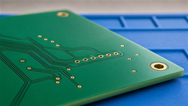
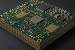
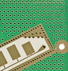
Close-up illustration of PCB ground copper, isolated signal pads and plated vias for layout review

Ground Plane Questions

1. Can a circuit board ground wire replace a plane?

A circuit board ground wire can provide a return connection in a suitable low-frequency or low-current circuit. It does not reproduce the broad, closely coupled reference of a plane for fast signals. Evaluate wire length, loop geometry and transient current, not just DC resistance.

2. Does a larger ground area always reduce noise?

No. A large area can still have narrow necks, unsuitable current sharing or poor connections between layers. Placement, continuity and the return-loop geometry matter more than copper coverage alone.

3. How is a ground plane antenna different?

A ground plane antenna intentionally uses a conductive reference as part of its radiating structure. An antenna ground plane may function as a counterpoise rather than simply as a shield. Design the ground plane for antenna operation together with the feed geometry and keepout. Flooding copper beneath every antenna is not a universal improvement.

For our RF printed circuit boards, material properties, reference spacing and copper geometry must be reviewed together. Ground copper useful beside an RF feed may still be prohibited in the antenna’s keepout region.

4. Do differential pairs need a reference plane?

Differential routing does not eliminate reference-plane considerations. Coupling between the pair, coupling to the plane, common-mode behavior and asymmetry all matter. Avoid routing the pair across an arbitrary reference gap merely because the signals are differential.

5. Can thermal reliefs be used on ground connections?

Yes, when their geometry meets electrical and assembly requirements. Thermal spokes can improve solderability, but their width and count also affect current capacity and impedance. High-current terminals and high-frequency connections may require a different attachment strategy.

Ground Plane Fabrication Support

We review manufacturability together with the specified stack-up and copper geometry. At EBest Circuit (Best Technology), our FR4 capability extends to up to 32 layers, and our HDI capability includes line/space down to 2/2 mil, subject to materials, board dimensions, stack-up and engineering review. These are capability limits, not default dimensions for every ground-plane design.

Our PCB manufacturing capabilities support construction planning, but finer traces and more layers do not guarantee a better return path. The finished board must preserve the reference geometry specified by the circuit design, and the assembled product still needs its appropriate electrical and EMC validation.

Conclusion

A useful circuit board ground plane is continuous where signals need it, connected where return currents change layers, and kept clear where isolation or antenna requirements demand it. Review the filled copper beneath critical routes, not just the GND net name. For stack-up and fabrication support, contact our team at sales@bestpcbs.com.


You may also like

What Is a Circuit Board Ground Plane in PCB Stackup?
Thursday, June 25th, 2026

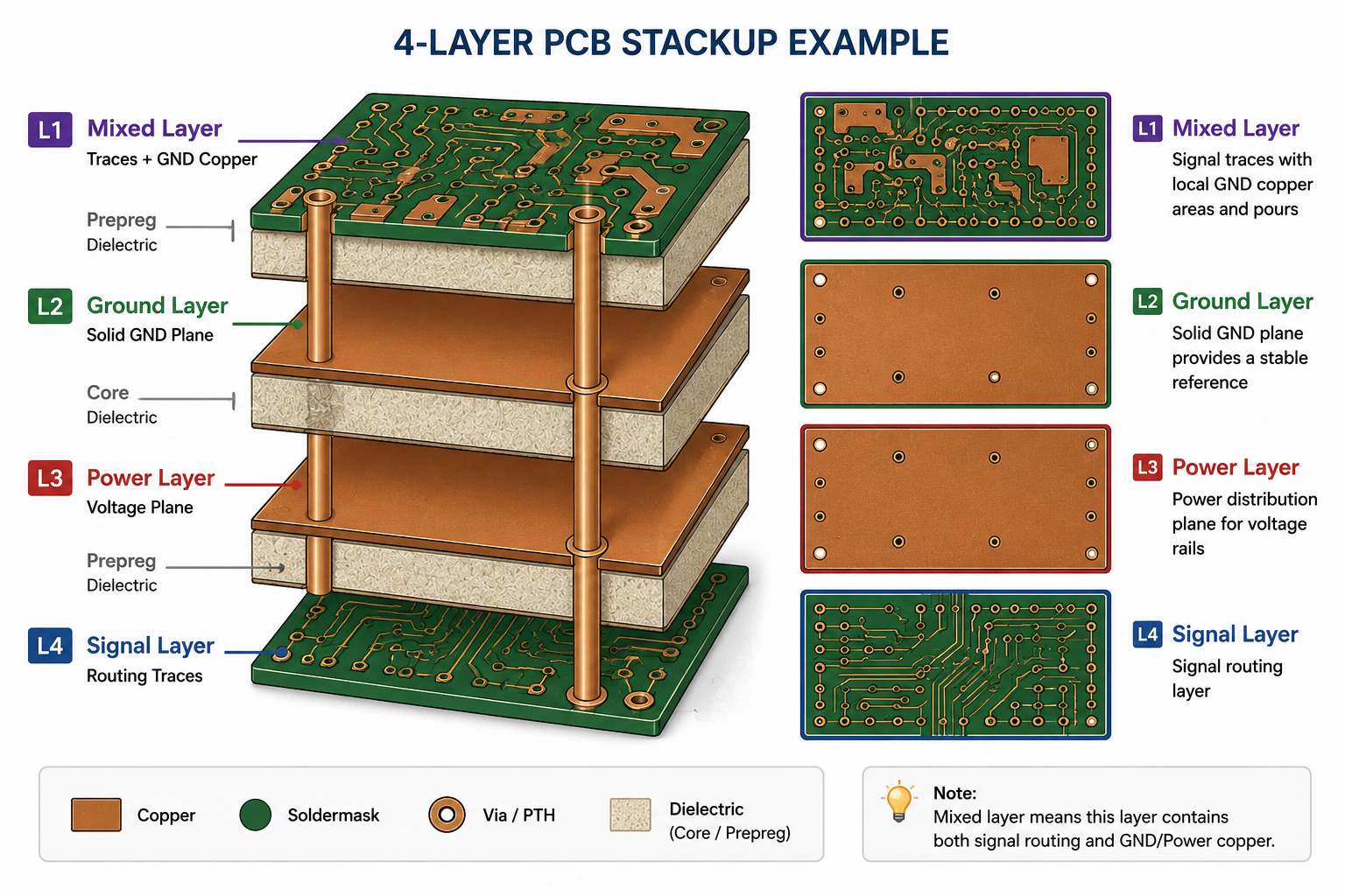
Circuit board ground plane is a key part of PCB stackup design, not just a large copper area connected to GND. It can be a bottom-side copper pour on a 2-layer PCB, a full internal ground layer in a multilayer PCB, or a mixed layer that combines GND copper with signal routing. For PCB and PCBA projects, the real question is not only what a ground plane is, but whether the design provides a stable ground reference for signal quality, EMC performance, impedance control, production reliability, and long-term use.

At EBest Circuit, also known as Best Technology, our engineering team helps customers review ground plane design together with PCB stackup, copper thickness, Core and Prepreg selection, impedance requirements, via structure, EMC risk, and manufacturability before production. We support FR4 PCB, high Tg PCB, impedance control PCB, heavy copper PCB, aluminum PCB, ceramic PCB, rigid-flex PCB, and turnkey PCBA services. If your project needs stackup review, grounding optimization, DFM checking, or PCB assembly support, please send your Gerber files, BOM, drawings, or technical requirements to sales@bestpcbs.com for a practical engineering review.

What Is a Circuit Board Ground Plane?

A circuit board ground plane is a copper area or copper layer connected to the GND net of a PCB. It provides a stable reference for signals and a low-impedance return path for current.

In a 2-layer PCB, the ground plane is usually a copper pour on one side of the board. In a 4-layer or multilayer PCB, it is often a dedicated inner ground layer. This dedicated layer is usually more stable because it is less interrupted by routing traces, pads, and component placement.

From a customer’s point of view, the most important thing is not whether the design has “some GND copper.” The key is whether the ground copper is continuous enough to support the signal, power, EMC, and manufacturing requirements of the product.

A ground plane should be reviewed together with PCB layer count, board thickness, copper thickness, Core, Prepreg, impedance requirements, via structure, and copper balance.

Why Does a Ground Plane Matter to PCB Buyers?

A good ground plane helps reduce electrical and production risks before the PCB enters fabrication.

  • For electrical performance, it provides a stable signal reference. High-speed traces, clock lines, RF circuits, ADC/DAC circuits, and communication interfaces all need a clean reference plane. If the reference is broken, the signal may become unstable, noisy, or difficult to control.
  • For EMC, the ground plane helps reduce current loop area. Smaller loop area usually means lower radiation and better noise control. This is important for industrial control, medical electronics, automotive electronics, power supplies, and products that need EMC testing.
  • For manufacturing, the ground plane also affects copper distribution and lamination. A large copper area may influence resin flow, board flatness, and copper balance. This is why PCB manufacturers check ground layers together with stackup and material structure, not only as an electrical net.

In short, the ground plane affects both how the PCB works and how the PCB is built.

How Do PCB Manufacturers Check the Ground Plane from Customer Files?

When a PCB factory reviews a project, engineers usually check Gerber or ODB++ files, drill files, stackup drawings, impedance tables, fabrication notes, and customer specifications together.

They mainly look for four things.

  • First, they confirm which layer is GND, which layer is power, and which layer is signal. If the layer naming is unclear, the engineering team may need to pause the review and ask the customer for confirmation.
  • Second, they check whether the ground plane is continuous under important signal traces. A high-speed trace routed over a split or broken ground plane may cause return path and EMI problems.
  • Third, they check whether the ground plane can support impedance control. Controlled impedance traces need a clear reference plane. If the reference plane has gaps or mixed copper, the final impedance may not match the expected value.
  • Fourth, they check whether copper distribution is manufacturable. Large copper areas, heavy copper, and uneven residual copper can affect lamination and warpage.

A complete file package helps reduce these questions. For complex boards, customers should provide Gerber or ODB++, drill files, stackup drawing, board thickness, copper thickness, impedance requirement, material notes, and any EMC or high-current requirements.

Ground Layer, Power Layer, Signal Layer, and Mixed Layer: What Should Customers Know?

In a PCB stackup, not every copper layer has the same purpose.

  • A Ground Layer is connected to GND and usually works as the main reference plane.
  • A Power Layer distributes voltage such as 3.3V, 5V, 12V, or other power rails.
  • A Signal Layer carries routing traces for digital, analog, RF, clock, or control signals.
  • A Mixed Layer contains signal routing together with GND or power copper.

This distinction is important because a mixed layer should not automatically be treated as a full ground plane. If signal traces cut through the GND copper, the return path may become less stable. If an impedance trace references a mixed layer with copper gaps, the impedance result may change.

For customers, the key check is simple: each important signal layer should have a clear and stable reference plane. This is especially important for high-speed, impedance-controlled, RF, and EMC-sensitive boards.

When Does a PCB Need a Dedicated Ground Plane?

Not every PCB needs a dedicated internal ground plane. Some simple products can work well with a 2-layer board and a good ground pour. But when the product has higher signal speed, higher current, stronger noise, or stricter EMC requirements, a dedicated ground layer becomes much more useful.

PCB ConditionBetter Ground Strategy
Simple low-speed board2-layer ground pour may be enough
Switching power circuitKeep power loop and GND return short
USB, Ethernet, HDMI, DDR, RFUse a dedicated ground layer
Controlled impedance PCBUse a clear reference plane
Medical, automotive, industrial PCBPrefer stable multilayer GND reference
Heavy copper or high-current PCBReview copper thickness, PP, and lamination

A 4-layer PCB is often a practical upgrade from a 2-layer PCB. A common structure is top signal layer, inner ground layer, inner power layer, and bottom signal layer. This gives important signals a nearby reference plane and makes EMC control easier.

For customers, the decision should not be based only on PCB unit price. If a 2-layer board causes repeated EMC failure, signal instability, or layout redesign, the total project cost may become higher than using a proper multilayer stackup from the beginning.

How Does the Ground Plane Affect Return Path and Impedance?

Every signal current needs a return path. In high-speed PCB design, the return current usually flows through the nearest reference plane, often directly under the signal trace.

If the signal has a continuous ground plane nearby, the return path is short and predictable. This reduces loop area, lowers radiation, and improves signal stability.

If the ground plane is cut, split, or missing under the trace, return current must detour. The trace may look fine in the layout, but electrically the loop becomes larger. This may cause EMI, crosstalk, impedance discontinuity, or unstable communication.

For impedance control, the ground plane is part of the transmission structure. Trace width, spacing, copper thickness, dielectric thickness, material dielectric constant, and distance to the reference plane all affect impedance. If the reference plane is not stable, impedance control becomes less predictable.

For layer changes, ground vias are also important. When a high-speed trace changes layers through a via, nearby GND vias help provide a clean return path between reference planes.

How Does a Circuit Board Ground Plane Affect EMC?

A circuit board ground plane affects EMC by controlling return current and reducing loop area. Large current loops behave like small antennas. When return current is forced to travel through a long or broken path, the PCB may radiate more noise.

This is where the importance of ground plane in PCB EMC design becomes clear. Ground plane design is not only about shielding. It also affects return current, common-mode noise, connector grounding, cable radiation, decoupling performance, and high-frequency stability.

Many EMC problems do not happen because the board has no GND. They happen because the GND path is poorly controlled. Typical examples include high-speed traces crossing split ground, switching current returning through a large loop, weak connector grounding, or shield copper with too few ground vias.

A good ground plane helps, but it cannot solve EMC alone. It must work with proper stackup, routing, decoupling capacitors, filtering, shielding, enclosure design, and cable grounding.

For PCBA projects, connector areas deserve special attention. Cables can easily become radiation paths. Stable ground copper, suitable via stitching, and a clear chassis ground strategy can reduce this risk.

Can a Large Ground Plane Create Manufacturing Problems?

Yes, if it is not reviewed properly.

  • A large ground plane is usually good for electrical performance, but it may affect manufacturing when copper distribution is unbalanced or copper thickness is high.
  • One concern is copper balance. If one layer has a nearly full copper plane while another layer has very little copper, the board may become less balanced during lamination. This can increase warpage risk, especially for thin, large, multilayer, or heavy copper boards.
  • Another concern is resin filling. For heavy copper ground planes, Prepreg resin must flow properly between copper areas during lamination. If the resin amount is not enough, the board may face voids, weak bonding, or reliability issues. When copper thickness reaches 2oz or above, the stackup may need higher-resin PP or a suitable PP combination.
  • Large ground copper can also affect soldering. Pads directly connected to large copper areas may lose heat quickly during assembly. For some pads, thermal relief can improve solderability. For high-current terminals, solid connection may still be required. The choice depends on current, heat, assembly, and reliability needs.

This is why a PCB manufacturer reviews the ground plane not only as a GND net, but also as part of the physical stackup.

What Ground Plane Mistakes Are Common in DFM Review?

Several ground plane issues often appear during DFM or engineering review.

  • A high-speed trace crosses a split ground plane. This breaks the return path and may create EMI or signal integrity problems.
  • A 2-layer board has too many traces cutting through the bottom GND copper. The board may pass continuity testing, but the return path becomes long and weak.
  • A copper island is left floating. Floating copper can pick up or radiate noise, so it should be removed or connected to GND with enough vias.
  • Ground vias are too few. Weak via connection between GND copper areas may reduce shielding and return path continuity.
  • Connector grounding is incomplete. Since cables can radiate noise, connector ground, shield pins, chassis ground, and nearby GND vias should be reviewed carefully.
  • Heavy copper GND is not matched with proper PP selection. This may increase resin filling or lamination risk.

These issues are not always obvious from a simple PCB screenshot. They require checking Gerber layers, stackup, copper distribution, via placement, and design intent together.

What Should Customers Confirm Before PCB Production?

Before production, customers should confirm the information that directly affects ground plane performance and manufacturability.

The most important items are board thickness, layer count, ground layer position, power layer position, copper thickness, Core and Prepreg structure, dielectric spacing, impedance requirements, via structure, material grade, and copper balance.

  • For controlled impedance boards, the customer should clearly state the impedance value, tolerance, routing layer, trace width, spacing, and reference plane.
  • For high-current PCB boards, the customer should mark current paths, finished copper thickness, via requirements, thermal pads, connector areas, and any special soldering needs.
  • For EMC-sensitive boards, the customer should provide grounding, shielding, connector, chassis ground, and testing requirements if available.
  • For special materials or non-standard stackups, early confirmation is important. Many PCB factories use common Core, PP, and copper foil materials to shorten lead time. Non-standard material may increase cost or delivery time.

Clear information helps the PCB manufacturer review the design faster and reduces repeated engineering questions.

FAQs about Circuit Board Ground Plane

Q1: What is a circuit board ground plane?
A circuit board ground plane is a copper area or copper layer connected to GND. It provides a stable reference and a low-impedance return path for current.

Q2: Is ground copper pour the same as a ground plane?
Not always. Ground copper pour can act as a ground area, especially on a double layer PCB. A dedicated ground plane usually means a more continuous copper layer in a multilayer PCB.

Q3: Does every PCB need a dedicated ground plane?
No. Simple low-speed PCBs may use ground pour only. High-speed, RF, controlled impedance, automotive, medical, and EMC-sensitive PCBs usually benefit from a dedicated ground layer.

Q4: Why does a ground plane matter for impedance control?
Controlled impedance traces need a clear reference plane. The trace width, copper thickness, dielectric spacing, and distance to the ground plane all affect impedance.

Q5: Can a power plane replace a ground plane?
Usually not. A power plane can sometimes act as an AC reference when properly coupled with ground, but it should not be treated as a direct replacement for a continuous ground plane.

Q6: Should analog ground and digital ground be split?
It depends on the circuit. Poorly split ground can break return paths and increase noise. Careful placement and controlled return current are often more important than simply cutting the ground plane.

Q7: What is PCB ground plane via stitching?
Via stitching means using multiple GND vias to connect ground copper across layers. It improves grounding, shielding, and return path continuity.

Q8: Can a large ground plane affect PCB manufacturing?
Yes. Large or heavy copper ground planes may affect copper balance, resin filling, lamination stability, warpage, and soldering behavior.

Q9: What should I send to a PCB manufacturer for ground plane review?
Send Gerber or ODB++ files, drill files, stackup drawing, board thickness, copper thickness, impedance requirements, material notes, and any EMC or high-current requirements.

In closing, a circuit board ground plane is not just a copper area connected to GND. For real PCB and PCBA projects, it affects stackup design, return path control, EMC performance, impedance stability, copper balance, solderability, and manufacturing reliability.

For simple low-speed boards, a 2-layer ground pour may be enough. For high-speed, RF, controlled impedance, medical, automotive, industrial, power electronics, or EMC-sensitive products, a dedicated ground layer in a clear multilayer stackup is usually the safer choice.

The most practical approach is to review the ground plane together with layer assignment, Core, Prepreg, copper thickness, dielectric spacing, via structure, impedance requirements, copper distribution, and DFM rules before production.

EBest Circuit, also known as Best Technology, provides PCB manufacturing and PCB assembly services for FR4 PCB, high Tg PCB, impedance control PCB, aluminum PCB, copper core PCB, ceramic PCB, heavy copper PCB, rigid-flex PCB, and turnkey PCBA. If your project needs stackup review, grounding optimization, impedance control, EMC improvement, or manufacturability checking, you can send your Gerber files, BOM, drawings, and technical requirements to our engineering team for a practical review.

You may also like