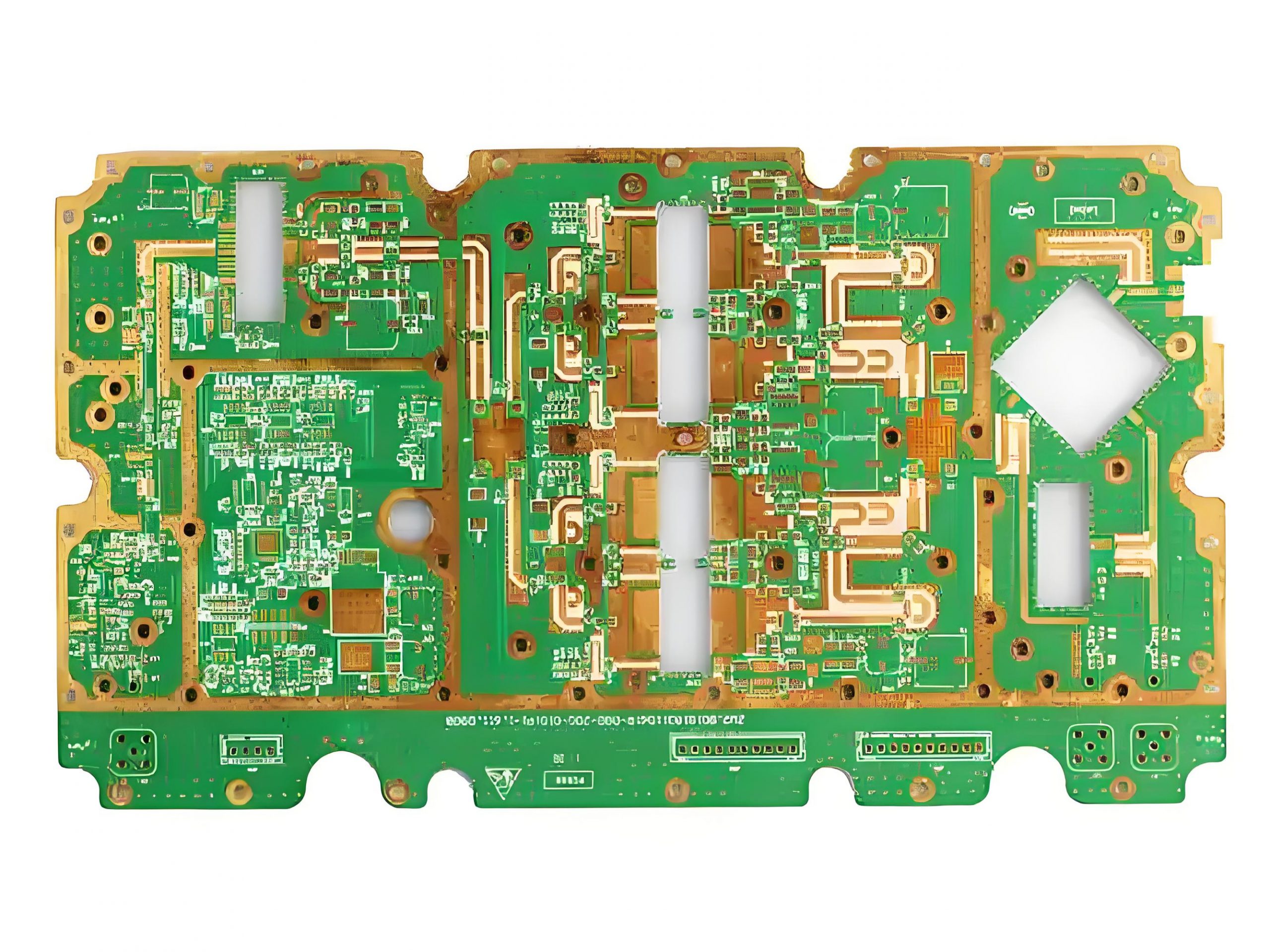
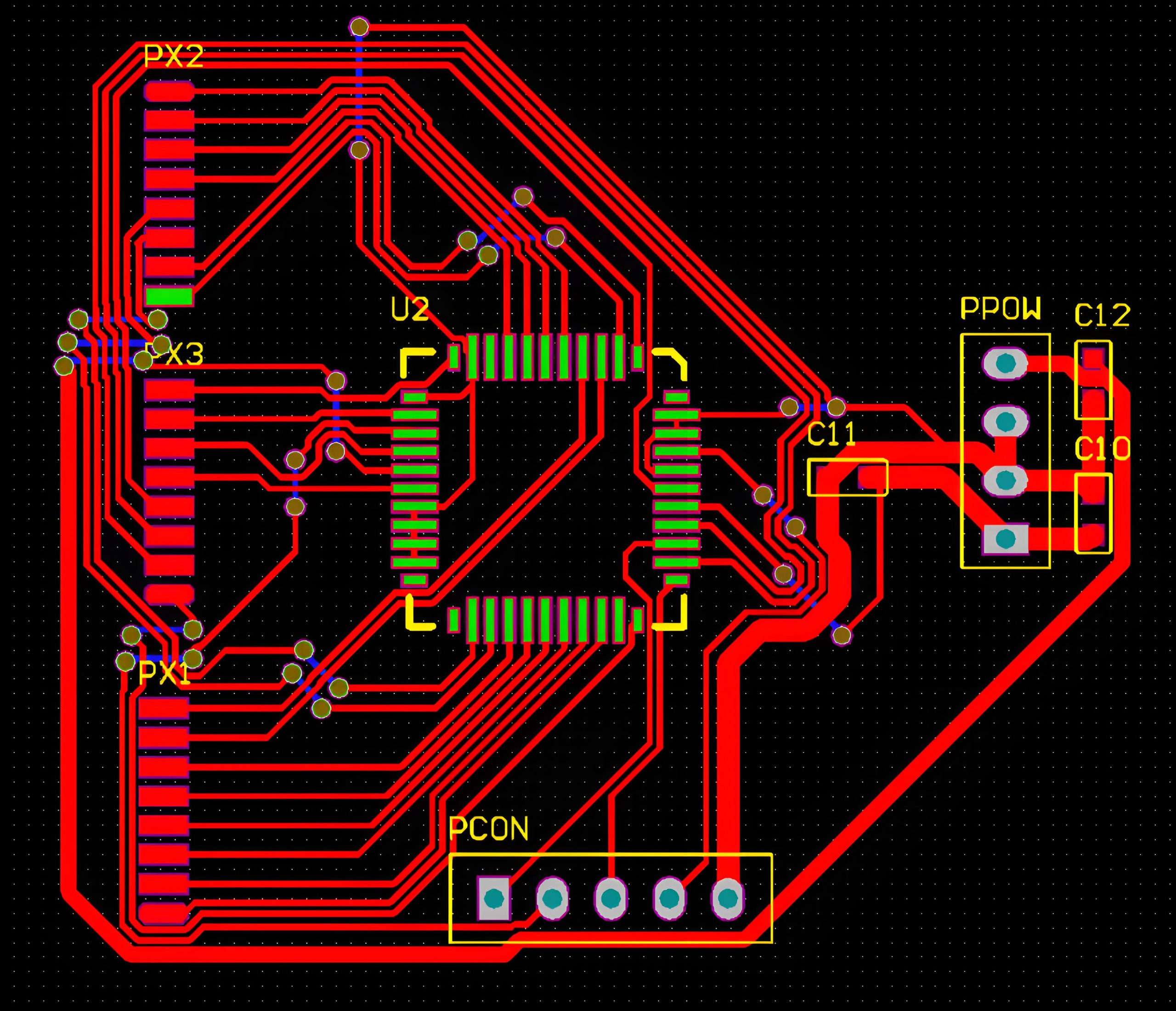
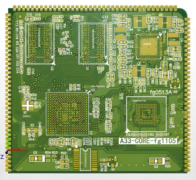
PCB manufacturing PCB manufacturing
Home > Blog

Basic Electron Devices and Circuits

June 27th, 2025

Electron devices and circuits are the foundation of modern electronics. From smartphones and computers to medical scanners and satellite systems, these components quietly manage the flow of electricity behind the scenes. This blog explores how they work, what types exist, and how they power the electronic world around us.

Basic Electron Devices and Circuits

What Are Electron Devices?

Electron devices are components that either control, modify, or amplify electrical signals. These devices rely on the movement of electrons to function and are used in countless applications, from simple toys to complex industrial machinery. Their job is to manage electrical energy in ways that produce useful output—such as turning on lights, processing data, or amplifying sound.

At their core, electron devices convert electrical energy into other forms or modify electrical signals to perform a specific function. Without them, modern electronic systems wouldn’t be possible.

Types of Electronic Devices

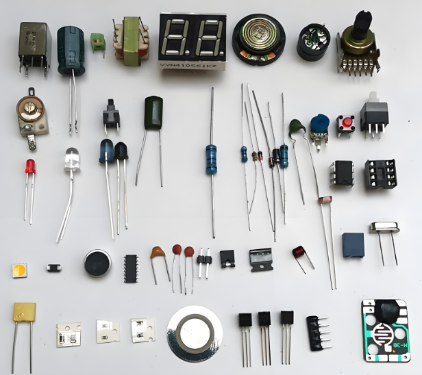
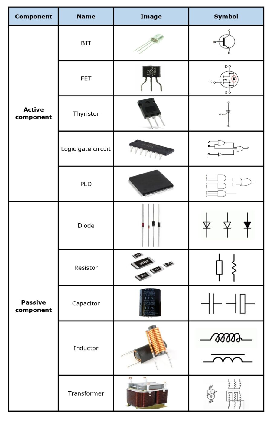
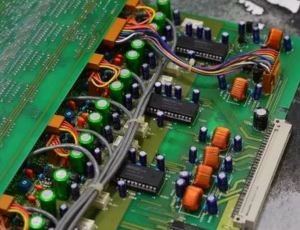
Each electronic component has specific properties that determine how it behaves in a circuit. The choice of components depends on the designer’s goal and the function the circuit is meant to perform. The image below highlights common electronic components used across various types of circuits. To better understand their roles, components are generally classified into two categories: Active Components and Passive Components.

1. Active Devices

    Active devices can control current flow and even amplify weak electrical signals. These devices require an external power source to operate. Some common active devices include:

    • Transistors: Used in amplifiers and switches.
    • Diodes: Let current flow in one direction.
    • Integrated Circuits (ICs): Tiny packages that contain complex electronic functions.

    Active devices are central to any system that processes signals, computes information, or boosts communication signals.

    2. Passive Devices

    Passive devices do not generate energy. Instead, they store, dissipate, or transfer it. Common examples include:

    • Resistors: Limit the flow of current.
    • Capacitors: Store and release electrical energy.
    • Inductors: Resist sudden changes in current.
    Types of Electronic Devices

    These components support the work of active devices and help shape how signals behave in a circuit.

    What Are the 5 Basic Electronic Devices?

    The five basic devices you’ll find in nearly every circuit are:

    • Resistor

    Resistors manage the current flowing through different parts of a circuit. They help in dividing voltage, controlling signal levels, and protecting components from excessive current.

    • Capacitor

    Capacitors store electrical charge temporarily. They’re used in filtering noise, smoothing power supply outputs, and creating time delays.

    • Inductor

    Inductors store energy in a magnetic field when current flows through them. They’re commonly used in filters, power supplies, and transformers.

    • Diode

    Diodes allow current to flow in only one direction. They are essential in power rectification, signal demodulation, and voltage regulation.

    • Transistor

    Transistors act as switches or amplifiers. They control the flow of current and are fundamental to logic circuits and digital electronics.

    How Do Electronic Devices Work?

    Each electronic device has a specific function based on its physical and electrical characteristics:

    • Resistors slow down current.
    • Capacitors store energy in an electric field.
    • Inductors build magnetic fields.
    • Diodes control direction.
    • Transistors regulate and amplify signals.

    Together, these devices shape how electricity behaves inside a circuit. When connected in specific arrangements, they form circuits capable of performing tasks like amplifying a sound, storing digital information, or controlling a motor.

    How Do Electronic Devices Work?

    What Are Electronic Circuits?

    An electronic circuit is a system of connected components that guide electrical currents to perform a specific job. These circuits can be as simple as a battery lighting an LED or as complex as the logic boards inside a computer.

    Circuits make electronic devices work by controlling where and how electricity flows. Each component in the circuit has a role—some store energy, others shape signals, and some respond to external inputs like light or sound.

    Types of Electronic Circuits

    Electronic circuits come in a few major types, depending on how they handle signals:

    • Analog Circuits

    Analog circuits work with continuous signals. They are used in audio systems, radio receivers, and temperature sensors. They process real-world inputs like sound or light.

    • Digital Circuits

    Digital circuits work with binary signals (0s and 1s). They form the backbone of computers, smartphones, and digital watches. Logic gates and microcontrollers are key components.

    • Mixed-Signal Circuits

    These combine analog and digital elements. Examples include digital audio converters, embedded controllers, and power management circuits.

    Types of Electronic Circuits

    Key Components in Electronics Circuits

    A functioning circuit depends on a combination of components, each with a distinct role:

    • Power Supply: Provides the necessary voltage and current.
    • Resistors: Manage current flow and protect sensitive parts.
    • Capacitors & Inductors: Shape or filter signals and manage timing.
    • Diodes & Transistors: Control signal direction, switching, and amplification.
    • Integrated Circuits (ICs): Combine multiple components in one small package for complex functions.
    • Switches, Connectors & PCBs: Physically support and route current throughout the system.

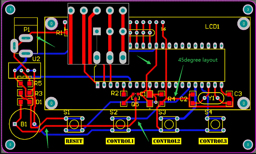
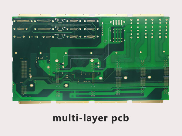
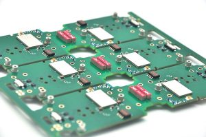
    All these parts are arranged on a printed circuit board (PCB), which provides the mechanical structure and electrical connections.

    Key Components in Electronics Circuits

    How to Design an Electronic Circuit?

    Designing a circuit starts with a clear goal. Once the purpose is defined, follow these steps:

    1. Outline Your Requirements: What do you want the circuit to do?
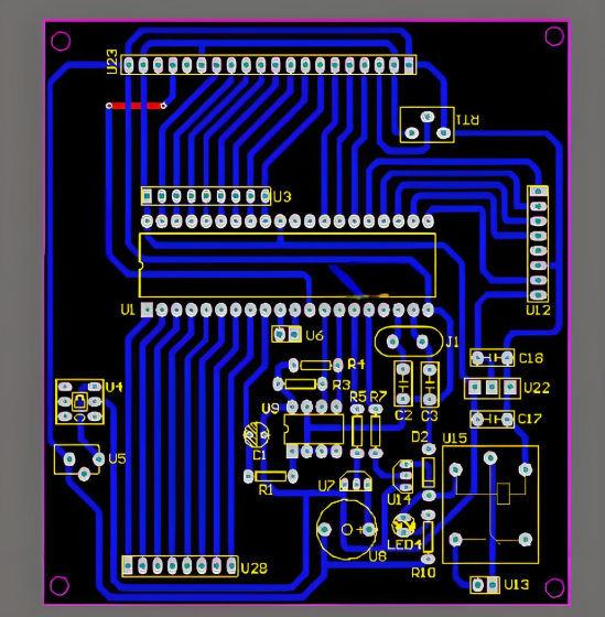
    2. Create a Schematic: Use circuit design software to build the layout using symbols for each component.
    3. Select Components: Choose values for resistors, capacitors, etc., based on your requirements.
    4. Simulate the Circuit: Check how it behaves using tools like LTspice or Proteus.
    5. Build a Prototype: Use a breadboard or PCB to assemble and test your design.
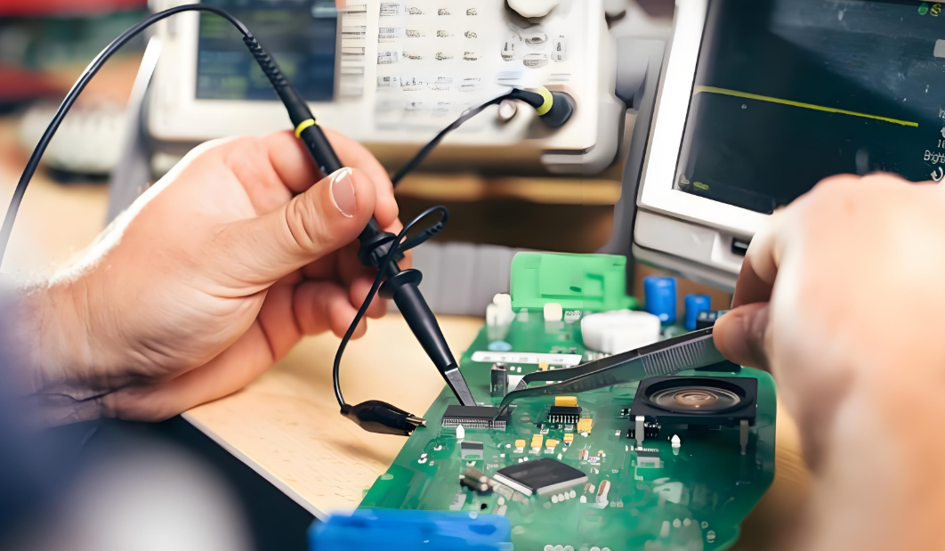
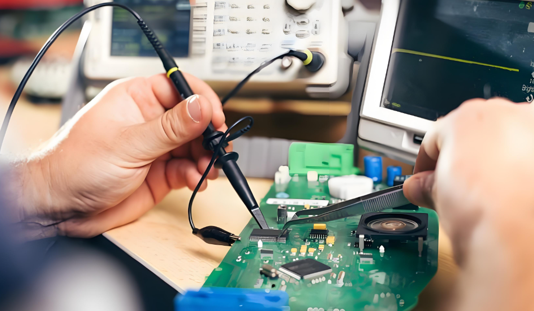
    6. Test & Debug: Measure voltages and currents to confirm it works as expected.
    7. Final Layout: Once tested, you can design a PCB for the final version.

    Even simple circuits need careful planning, as incorrect wiring or value choices can lead to failure or inefficiency.

    Common Measurement Devices for Electronic Circuits

    To check and troubleshoot circuits, engineers use various tools:

    • Multimeter: Measures voltage, current, and resistance. Essential for almost any testing.
    • Oscilloscope: Displays how signals change over time—helpful for analyzing waveforms.
    • LCR Meter: Measures inductance (L), capacitance (C), and resistance (R).
    • Logic Analyzer: Helps in debugging digital signals and timing issues.

    These devices ensure that the circuit performs properly under different conditions.

    Applications of Electron Devices and Circuits

    Electron devices and circuits power virtually all technology we use today. Here are a few major application areas:

    • Consumer Electronics: Televisions, phones, game consoles, and home appliances all rely on sophisticated circuits.
    • Automotive Systems: Used in engine control units (ECUs), ABS brakes, GPS modules, and more.
    • Medical Devices: Circuits manage everything from heart monitors to imaging systems.
    • Telecommunications: Signal boosters, routers, and network devices depend on electronic components.
    • Industrial Equipment: Used in automation, robotics, and machine control systems.
    • Defense & Aerospace: Critical in radar systems, flight control computers, and satellite communications.

    No matter the industry, the role of electron devices and circuits is critical in innovation, performance, and safety. Whether you’re a student, hobbyist, or professional, grasping how circuits function and how devices interact is essential to designing or repairing electronic equipment.

    For those looking to build reliable circuit boards or need help bringing their electronic designs to life, partnering with an expert manufacturer is key.

    Why Choose EBest Circuit (Best Technology) for Electronic Circuit Projects?

    EBest Circuit (Best Technology) is a trusted PCB manufacturer specializing in both prototype and volume production. With ISO-certifications, our team ensures your circuits meet international standards. Whether you need rigid PCBs, flexible circuits, or mixed-signal board assemblies, we help turn your ideas into high-quality products—on time and within budget. By choosing EBest Circuit (Best Technology), you can enjoy:

    1. Fast Turnaround from Prototype to Mass Production

    We help you move quickly from design to final product. Whether it’s a first-run prototype or a full production batch, we adapt to your schedule and keep your project on track.

    2. Hands-On Engineering Support

    Our experienced engineers work with you on component selection, stack-up optimization, and layout suggestions—helping you avoid design flaws before production begins.

    3. High Customization, No Fear of Complexity

    Need a non-standard stack-up, hybrid materials, or bendable structures? We handle complex builds with confidence and tailor every detail to match your design requirements.

    4. Clear Quotes and On-Time Delivery

    Our pricing is transparent, and our timelines are realistic. Dedicated project coordinators provide regular updates, so you’re never left guessing.

    5. Quality is a Daily Practice, Not Just a Promise

    We don’t just inspect a few boards—we test every unit. From flying probe tests to X-ray and AOI, our quality process ensures every board performs reliably.

    FAQs

    1. What’s the difference between an electronic and electrical device?

    Electronic devices use the flow of electrons to process signals, while electrical devices typically handle power distribution and energy conversion.

    2. Can I build electronic circuits without a PCB?

    Yes, prototypes are often built on breadboards or perfboards, but PCBs are used for stability and durability in final products.

    3. What software is best for circuit design?

    Popular tools include KiCad, Eagle, Altium Designer, and Proteus for simulation and layout.

    4. What is the most common cause of circuit failure?

    Overheating, poor soldering, incorrect component values, or voltage surges are common failure causes.

    5. How do I start learning electronics as a beginner?

    Start with basic components, build simple circuits using breadboards, and gradually move to microcontroller projects using kits like Arduino or Raspberry Pi.

    You may also like

    Flexible Foldable PCB: Types, Advantages & Applications

    June 26th, 2025

    Foldable PCB technology has changed how engineers design compact and flexible electronics. From smartphones that fold in half to medical devices that wrap around the body, a foldable PCB board helps make these designs possible. Unlike traditional rigid boards, these PCBs bend or twist without breaking. They save space, reduce weight, and often need fewer connectors.

    In this blog, we’ll explore different types of foldable PCBs, their pros and cons, where they’re used, and why certain types—like bendable aluminum—cost more. We’ll also share the key design tips and how to find a reliable foldable PCB manufacturer for your next project.

    What is a Foldable PCB?

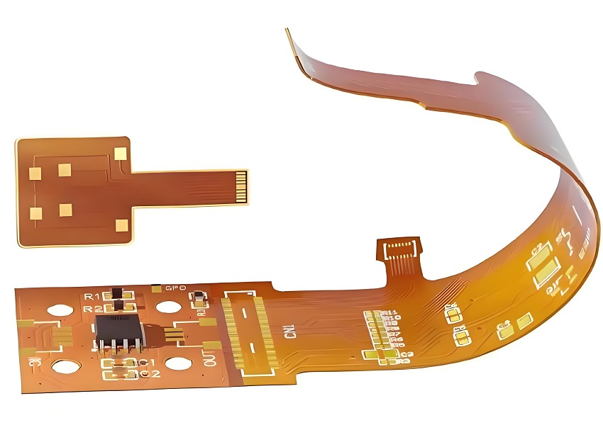
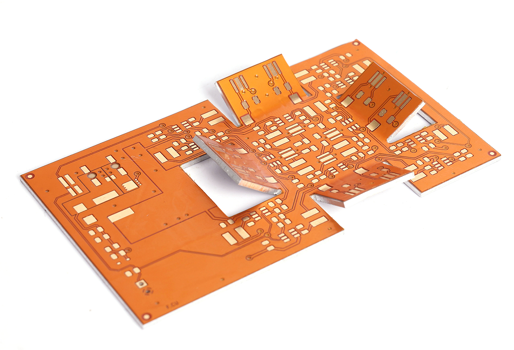
    A foldable PCB is a printed circuit board designed to bend, flex, or fold without damaging the electrical pathways. These PCBs are made using flexible materials like polyimide or specially treated FR4. They are often thin, light, and durable, which makes them useful in tight or moving spaces.

    Unlike rigid boards, foldable PCBs can take on 3D shapes. They can be used in hinges, curves, or tight enclosures where a regular FR4 PCB won’t fit. These designs cut down on cables and connectors, making the device smaller, lighter, and more reliable.

    What is a Foldable PCB?

    Foldable PCB Types

    Foldable PCBs come in several forms. Each has its own strength and is used in different applications.

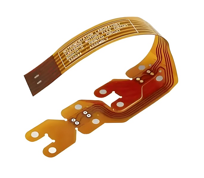
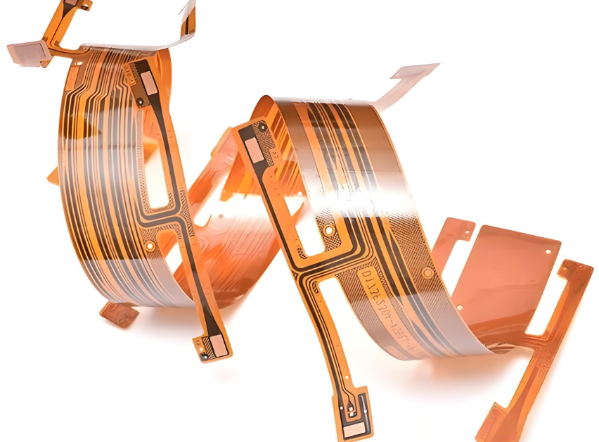
    • Flexible Circuits

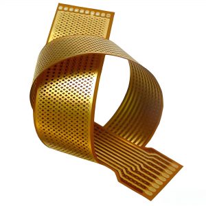
    This is the most common flexible circuits, called FPC as well. These use a thin polyimide film instead of standard fiberglass. They can bend freely in any direction and are ideal for cameras, printers, wearables, and foldable phones. They’re often single-sided but can be multilayered.

    Flexible Circuits
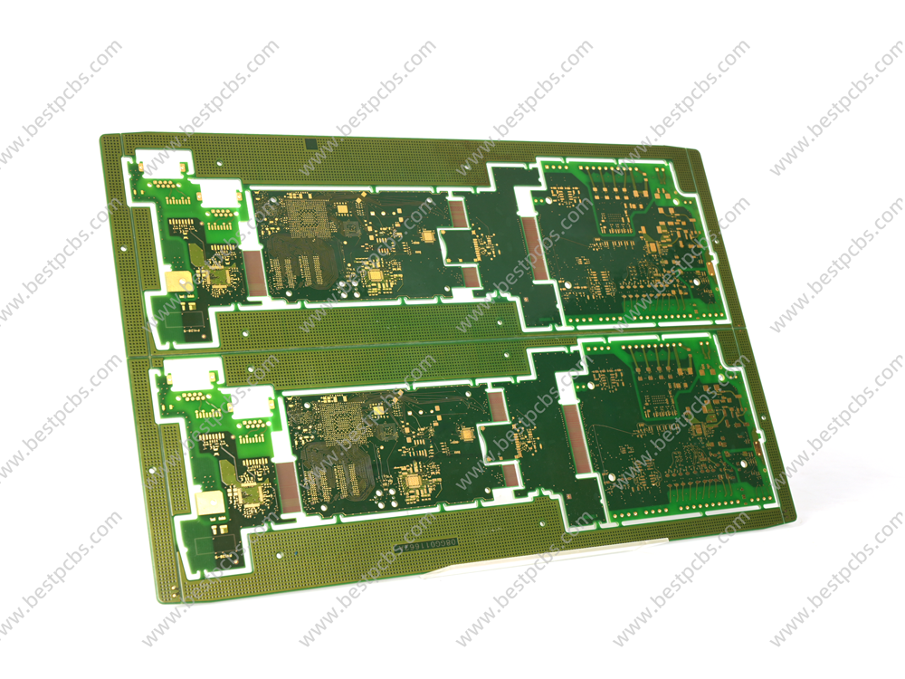
    • Rigid-Flex PCBs

    A rigid-flex PCB combines the best of both worlds—rigid sections for stable component mounting and flexible areas to allow folding. These are popular in complex devices like military gear, satellites, and high-end medical tools.

    Rigid-Flex PCBs
    • Semi-Flexible PCBs

    Semi-flexible PCB uses a flexible version of standard FR4. It’s bendable only once or twice during installation. It’s cheaper than flex PCBs but more limited. You’ll find these in LED modules or automotive electronics where minor bending is needed.

    Semi-Flexible PCBs
    • Bendable Aluminum PCBs

    Bendable aluminum boards use aluminum cores with bendable material series. They are mostly used in LED strips, vehicle lighting, or static fold setups. While they aren’t as flexible as polyimide boards, they handle heat well and provide strong mechanical support.

    Bendable Aluminum PCBs

    Advantages of Foldable PCBs

    • Saves space: They fit in tight spots and allow for creative layouts.
    • Reduces weight: Ideal for portable or wearable devices.
    • Fewer connectors: Fewer mechanical connections mean fewer failure points.
    • Shock resistance: Flex PCBs can absorb vibrations better than rigid ones.
    • Better reliability: Strong signal paths without added cables.

    Disadvantages of Foldable PCBs

    • Higher cost: Especially true for rigid-flex or aluminum options.
    • Complex design: Requires careful layout and material selection.
    • Bending fatigue: Repeated flexing can wear out traces over time.
    • Limited layer options: Fewer layers compared to rigid boards.

    Foldable PCB Applications

    Foldable PCB boards are now used across many industries thanks to their size and flexibility. Common applications include:

    • Smartphones and tablets: Especially foldable or flip models.
    • Wearable devices: Smartwatches, health bands, or fitness trackers.
    • Medical devices: Flexible sensors, hearing aids, or body patches.
    • LED lighting systems: Flexible LED strips, curved lighting, or signage.
    • Automotive interiors: For dashboards, control panels, and ambient lighting.
    • Consumer electronics: Cameras, game controllers, or fold-out gadgets.
    • Aerospace and military: Lightweight systems that must handle vibration.
    Foldable PCB Applications

    Why Bendable Aluminum PCB Costs More Than Flexible Circuits?

    You might notice that bendable aluminum PCBs often cost more than regular flexible circuits. Here’s why:

    • Material cost: Aluminum cores and dielectric layers used in bendable boards are more expensive than polyimide film used in flex PCBs.
    • Thermal performance: These boards are built for high-heat environments, so they require special treatment and thermal interface materials.
    • Machining difficulty: Bending metal without damaging the circuit paths takes precision and specialized tools.
    • Lower yield rate: These boards are harder to process in large volumes, especially when custom bending angles are needed.

    So while bendable aluminum PCBs offer great heat management and durability, their manufacturing process drives up the cost compared to standard flexible circuits.

    Design Considerations of Foldable PCB Board

    When designing a foldable PCB, there are several rules to follow:

    • Bend radius: Always keep the bend radius at least 6 to 10 times the board thickness to avoid cracks or delamination.
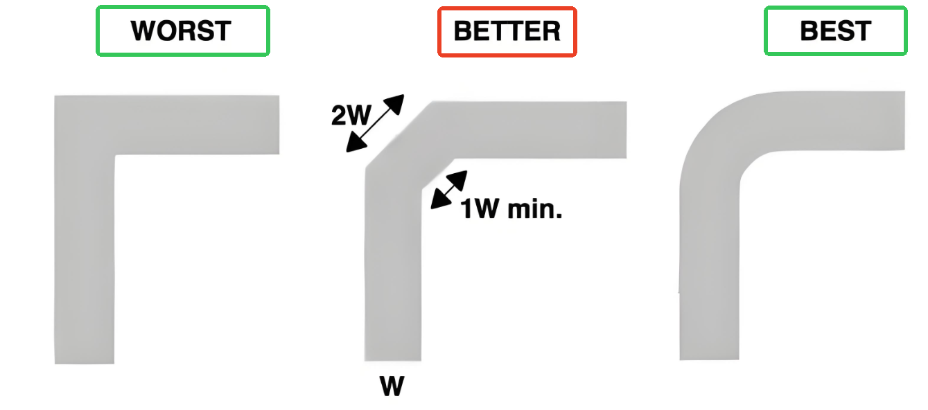
    • Trace layout: Avoid sharp corners or 90-degree bends in traces, especially in flexible sections. Use curved paths for less stress.
    • Stress relief: Add slots or wider copper pads in flex areas to reduce strain.
    • Material selection: Choose polyimide for high flex use or semi-flex FR4 for limited bends. For heat-heavy setups, use bendable aluminum.
    • Stack-up planning: Place sensitive components away from fold zones. Keep fewer layers in the flex area to maintain reliability.
    • Bending direction: Plan the layout to avoid stress on solder joints or component leads when the board is bent.

    Designing for foldability takes extra care, but it pays off in product performance and durability.

    Where to Find a Foldable PCB Manufacturer?

    If you’re building devices with foldable designs, it’s important to work with a manufacturer that understands the details. Here’s what to look for:

    • Specialized experience: Choose a factory with proven capability in flex, rigid-flex, and semi-flex designs.
    • Engineering support: You’ll need layout reviews, DFM checks, and prototyping advice.
    • Clean production: Flex and bendable PCBs need precise etching and lamination in controlled environments.

    EBest Circuit (Best Technology) is one of the leading manufacturers offering complete support for foldable PCB boards. At EBest Circuit (Best Technology), “Total Customer Satisfaction” is our goal, and it is the core of EBest Circuit (Best Technology)’s operation as a PCB manufacturer. Procurement, sales, engineering, manufacturing, inventory, and quality have the same common goal of ensuring directly or indirectly “Total Customer Satisfaction”. We provide flexible circuit production, rigid-flex builds, and even custom aluminum-based PCBs for thermal control. With our ERP traceability system and professional engineering team, we help clients go from prototype to mass production with speed and reliability.

    Call To Action

    Get in touch with us today for a quick quote or engineering consultation—we’ll help bring your folding design to life.

    FAQs

    Q1: Can foldable PCBs be reused after bending?

    Some types, like polyimide flex circuits, can bend thousands of times. Others, like semi-flex or bendable aluminum PCBs, are designed for limited bending during assembly.

    Q2: What’s the lifespan of a flexible PCB?

    With proper design, a flex circuit can last over a million bending cycles. It depends on material, bend radius, and stress exposure.

    Q3: Are foldable PCBs safe for high-current applications?

    Yes, with the right trace width and copper thickness. However, heat management and durability must be carefully planned.

    Q4: Can I mount heavy components on the flexible part?

    No. Heavy or rigid components should be placed on the rigid or reinforced sections to avoid stress damage.

    Q5: How fast can I get a foldable PCB prototype?

    At EBest Circuit (Best Technology), we offer fast-turn prototyping in as little as 5–7 working days, depending on design complexity.

    When you’re ready to build a reliable and high-performance foldable circuit, EBest Circuit (Best Technology) is here to help. Our expert team, quality certifications, and full-service support make us the go-to foldable PCB manufacturer in China.

    You may also like

    What is DTP MCPCB? DTP Copper MCPCB Structure

    June 25th, 2025

    A DTP MCPCB, or Direct Thermal Path Metal Core PCB, also known sinkpad MCPCB, is a type of printed circuit board designed for high-power and high-heat applications. It helps electronics stay cool and stable, even under heavy loads. Compared to standard MCPCBs, DTP PCBs offer better thermal transfer and stronger mechanical support. Many industries, including LED, power supply, automotive, and telecom, now prefer DTP copper MCPCBs for reliable performance.
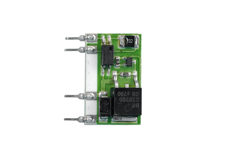
    In this blog, we’ll explain what DTP means, its features, structure, design tips, manufacturing process, and how it fits into modern electronics.

    What Is DTP and Its Features?

    DTP stands for Direct Thermal Path. It refers to a design where heat moves directly from hot components to the metal base without many thermal barriers. This path lowers thermal resistance and keeps components cooler.

    Main Features of DTP:

    • Direct connection between heat source and metal base
    • Higher heat dissipation than traditional MCPCBs
    • Stronger thermal conductivity through thick copper or copper convexity
    • Better reliability in high-power circuits
    • Long-lasting even under thermal cycling and vibration

    This structure reduces the chance of overheating, which helps the whole system run longer and safer.

    What is DTP MCPCB? DTP Copper MCPCB Structure

    DTP Copper MCPCB Structure

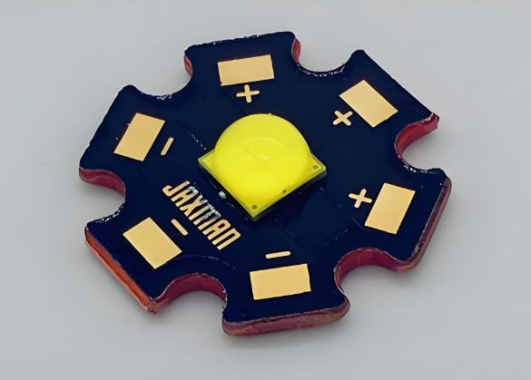
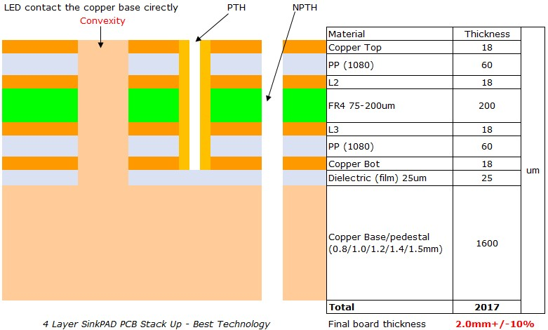
    A DTP copper MCPCB uses a raised copper structure (called a copper convexity or copper boss) formed directly on the metal base. This convex feature aligns under the heat source, typically a power component like a MOSFET or high-wattage LED. The DTP copper PCB layers are:

    • Top Layer: Copper trace for electrical routing
    • Dielectric Layer: High thermal conductivity insulation
    • Copper Convexity: Directly contacts both the component and the base
    • Metal Base: Usually aluminum or copper for heat spreading

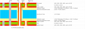
    Its stackup layers is:

    What is DTP MCPCB? DTP Copper MCPCB Structure

    This design bypasses traditional insulation layers and allows heat to flow directly into the metal core.

    DTP MCPCB vs Traditional MCPCB

    Standard MCPCBs have a thin dielectric layer between the copper trace and the metal base. This layer adds thermal resistance. In contrast, a DTP PCB reduces this resistance by forming a direct path between the component and the base metal using copper convexities.

    FeatureDTP MCPCBTraditional MCPCB
    Heat TransferDirect (through copper convexity)Through dielectric
    Thermal ResistanceVery LowMedium
    Use CaseHigh-power, LED, EV, power supplyGeneral LED, moderate power
    CostHigherLower
    PerformanceExcellentGood

    Where Are DTP PCBs Used?

    DTP MCPCBs are perfect for any application where heat is a big issue. They’re now standard in many thermal-critical products. The main applications including:

    • High-power LED lighting
    • Power supplies and inverters
    • Electric vehicles (EVs) and battery packs
    • RF and telecom base stations
    • Solar energy systems
    • Laser modules and sensors

    Whenever components get hot and space is tight, DTP copper MCPCBs offer a smart solution.

    Tips for MCPCB Design with DTP Structure

    Designing a DTP PCB requires special attention to thermal paths, layout, and material selection.

    1. Place heat-generating components directly over copper convexities
    2. Use high-conductivity dielectric materials to keep thermal resistance low
    3. Align thermal vias with component pads for effective heat flow
    4. Choose a suitable base material: aluminum for cost, copper for performance
    5. Ensure planarity and flatness for solid thermal contact

    A carefully designed DTP MCPCB handles more power without compromising safety or reliability.

    Why Is the Price of DTP MCPCB Higher Than a Normal MCPCB?

    The cost of a DTP MCPCB is higher due to the complexity of its design and processing. It uses thicker copper or custom copper convexities, which are more expensive than standard copper foil. Creating a precise raised copper feature under each heat source requires extra machining steps, tight alignment, and rigorous quality checks.

    Additionally, the dielectric materials used must have very high thermal conductivity and are usually more costly. The manufacturing process also involves advanced methods like X-ray alignment, CNC machining, and thermal performance testing. Despite the higher price, DTP MCPCBs offer long-term savings by improving thermal efficiency, reducing failure rates, and extending product lifespan.

    How DTP MCPCBs Are Manufactured?

    The manufacturing of a DTP MCPCB is more advanced than a standard MCPCB manufacturing process. It focuses on forming a raised copper boss (convexity) that provides a one-piece thermal bridge between the heat source and the metal base.

    1. Base Metal Preparation

    The aluminum or copper base is cleaned and pre-treated. This forms the foundation for the entire board.

    2. Creating the Copper Convexity

    A raised copper feature is formed on the base metal. This copper boss is placed directly beneath high-heat components. The convexity may be CNC machined or created during the copper plating process.

    3. Dielectric Layer Lamination

    A thin, high-thermal-conductivity dielectric is laminated around the copper convexity and onto the metal base. The copper bump remains exposed to make direct contact with the top copper circuit.

    4. Copper Foil Application & Circuit Etching

    Copper foil is laminated onto the surface and patterned using photolithography. The exposed part of the copper boss connects directly to a pad on the top layer.

    5. Drilling & Plating (if required)

    If the design includes signal vias or multi-layer connections, micro-drilling and copper plating are applied carefully to avoid damaging the copper boss.

    6. Solder Mask & Surface Finish

    Solder mask is printed, leaving heat transfer pads exposed. Surface finish (e.g., ENIG, HASL) is applied for soldering protection.

    7. Inspection & Testing

    • X-ray confirms alignment of copper convexity under the pad
    • Thermal resistance is measured
    • Electrical continuity is tested
    • Visual and mechanical checks ensure no delamination or defects

    This process requires tight process control and high-end fabrication equipment.

    Benefits of Using DTP Copper MCPCB in High-Power Electronics

    • Superior thermal performance for high-wattage components
    • Longer component life due to reduced junction temperatures
    • Smaller form factor with higher power density
    • Stable performance under vibration, shock, and thermal cycling
    • Improved system efficiency and lower cooling requirements

    These benefits make DTP MCPCBs an excellent investment for demanding applications.

    What is DTP MCPCB? DTP Copper MCPCB Structure

    DTP PCB Material Choices

    A high-quality DTP PCB relies on the right materials:

    • Copper Convexity: Pure copper, usually 1–4mm thick
    • Dielectric Layer: Ceramic-filled epoxy or other high-conductivity material

    Metal Base:

    • Aluminum: Lightweight, good for general use
    • Copper: Best thermal conductivity, ideal for extreme conditions

    The right combination depends on your project needs, thermal limits, and cost targets.

    Why Work With a Reliable DTP MCPCB Manufacturer?

    Not all PCB manufacturers can build DTP MCPCBs. You need a supplier with tight process control, CNC machining, and advanced lamination tools.

    A good DTP supplier should offer:

    • Custom DTP MCPCB design support
    • In-house thermal simulation and analysis
    • CNC or stamping for copper convexity
    • X-ray and AOI for high-precision quality control
    • Quick prototyping and scalable volume production

    About EBest Circuit (Best Technology)

    At EBest Circuit (Best Technology), we are experts in DTP MCPCBs, aluminum PCBs, and thermal solution boards. We serve industries including LED, automotive, telecom, and medical electronics. We also use MES systems to provide full traceability of materials and processes. Our team can support you from design to mass production with reliable engineering and fast service.

    Call To Action

    If you’re working on a demanding project, contact EBest Circuit (Best Technology) to learn how a custom DTP copper MCPCB can power your next innovation.

    FAQs

    1. What is a DTP MCPCB?

    A Direct Thermal Path MCPCB uses a raised copper convexity to transfer heat directly from the component to the metal base.

    2. How does a DTP copper MCPCB differ from a standard one?

    It bypasses insulating layers by forming a direct copper path, reducing thermal resistance.

    3. What are the main uses of DTP PCBs?

    Used in LED lighting, power supplies, automotive electronics, and telecom base stations.

    4. Why is the DTP MCPCB more expensive?

    It uses more copper, complex machining, high-end materials, and tighter quality control.

    5. Does EBest Circuit (Best Technology) offer custom DTP MCPCB services?

    Yes, we provide full engineering support, fast prototyping, and scalable production.

    You may also like

    IMS PCB Full Form, Insulated Metal Substrate PCB Manufacturer

    June 24th, 2025

    IMS PCB full form is Insulated Metal Substrate PCB—a type of printed circuit board built to manage high heat and maintain strong mechanical support. It’s a popular choice for LED lighting, power supplies, and automotive electronics, where heat control is critical.
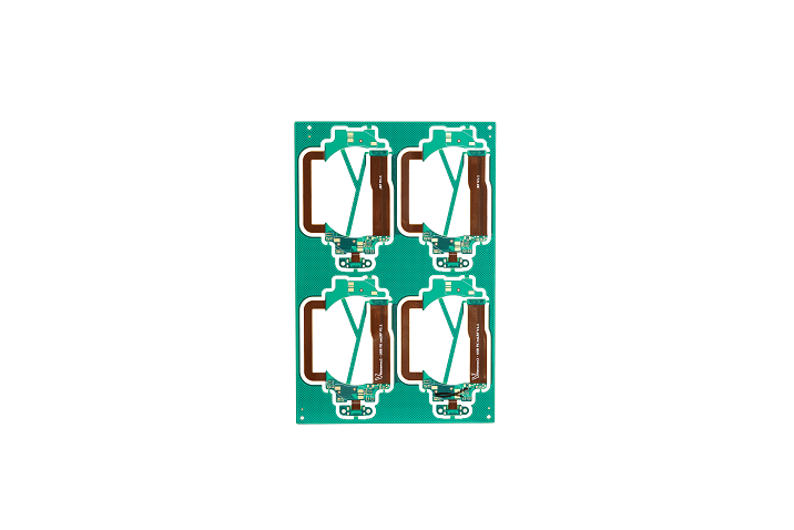
    At EBest Circuit (Best Technology), we’re a trusted IMS PCB manufacturer in China, providing custom thermal management solutions with high precision, reliable materials, and a full range of engineering support. But let’s dig deeper into what makes insulated metal substrate PCBs unique—and why they’re so important in modern electronics.

    IMS PCB Full Form, Insulated Metal Substrate PCB Manufacturer

    What Is IMS Insulated Metal Substrate PCB?

    An IMS (Insulated Metal Substrate) PCB is a type of circuit board that uses a thermally conductive dielectric layer bonded between a metal base (often aluminum or copper) and a copper circuit layer. The metal base helps dissipate heat more efficiently, especially compared to traditional FR4 boards.

    When it comes to IMS PCB thermal conductivity, this is the most valuable feature. The dielectric layer in IMS boards typically offers a thermal conductivity range from 1.0 W/mK to over 8.0 W/mK, depending on the application. The metal base, like aluminum or copper, works as a built-in heat sink—pulling heat away from active components like LEDs, power transistors, or ICs. That’s why IMS PCBs are commonly used in LED modules, power converters, automotive lighting, and solar inverters—where both heat and performance need to be tightly controlled.

    IMS PCB Material

    Choosing the right material for an IMS board is essential. Three layers make up a standard IMS PCB: the metal base, the dielectric layer, and the copper foil. And for the metal base, there are two options: copper base and aluminum base.

    • Copper IMS PCB

    Copper IMS PCBs offer superior heat transfer capabilities. Copper has a thermal conductivity of nearly 400 W/mK, much higher than aluminum. This means copper is ideal for applications with extreme power densities or where space is limited but heat is a concern.

    However, copper is also more expensive and heavier than aluminum, so it’s generally reserved for high-performance needs like laser modules, RF circuits, or military-grade devices.

    Copper IMS PCB
    • IMS Aluminum PCB

    The IMS aluminum PCB is the most common choice. Aluminum provides good thermal conductivity (typically around 200 W/mK), excellent mechanical strength, and lower cost compared to copper.

    Aluminum IMS PCBs are often used in LED lighting systems, electric vehicle chargers, power control modules, and industrial automation systems. They provide a balanced solution between cost and thermal management, which is why they’re the industry standard. Some common aluminum grades used include:

    • 5052 aluminum: Strong, corrosion-resistant, and suitable for structural use.
    • 6061 aluminum: Versatile, high-strength alloy.
    • 1060 aluminum: Excellent thermal conductivity, ideal for cost-sensitive applications.
    IMS Aluminum PCB

    IMS PCB Stackup

    The stack-up of an IMS PCB refers to how the layers are arranged. A typical IMS PCB stackup includes:

    • Top copper trace layer – for routing signals and power.
    • Thermal dielectric layer – usually made of epoxy resin filled with ceramic for heat transfer.
    • Metal base – usually aluminum or copper.

    For more advanced applications, 2 layer IMS PCBs are often used. In a 2 layer IMS PCB, an additional copper circuit layer is placed above the dielectric, and interconnections are formed using plated through-holes. These are useful when you need more complex routing or higher power density.

    Multilayer IMS stackups are possible but require special lamination techniques. These are often customized depending on the mechanical, electrical, and thermal needs of the application.

    IMS PCB Applications

    Thanks to their excellent thermal performance and mechanical strength, IMS PCBs are widely used in demanding environments. Here are some key application areas:

    • LED lighting: Street lights, high-bay lights, grow lights, automotive headlights.
    • Power electronics: DC-DC converters, voltage regulators, motor drivers.
    • Automotive systems: Electric vehicle controllers, battery management units.
    • Industrial equipment: Robotics, welding machines, servo drivers.
    • Telecommunication: 5G base stations, power amplifiers.
    • Renewable energy: Solar panel inverters, wind turbine converters.

    IMS PCB HS Codes

    For companies that export or import IMS PCBs, understanding HS codes (Harmonized System codes) is essential for customs clearance and compliance.

    The general HS Code for IMS PCB falls under:

    8534.00 – Printed Circuits

    Subcategories can vary depending on whether the board is populated (assembled) or bare.

    To be more precise:

    a. Bare IMS PCBs (unassembled):

    • HS Code 8534.00.90 (for 1-4 layer ims pcb)
    • HS Code 8534.00.10 (4 or above layer ims pcb)

    b. Assembled IMS PCBs:

    HS Code 8537.10 or others depending on final product classification and applications.

    Always check with your local customs authority or logistics provider for the exact code applicable to your product type and destination country.

    IMS PCB Assembly

    IMS PCB assembly involves more care than standard FR4 boards due to thermal management and mechanical rigidity. Special attention must be given to soldering profiles and thermal expansion to prevent cracking or delamination.

    Key points during assembly:

    • Use low-stress soldering methods (e.g., vapor phase or controlled reflow).
    • Ensure proper thermal profile during reflow to avoid damage to the metal base or insulation.
    • Choose high-Tg solder masks and components to handle high power density applications.

    For high-volume needs, automated SMT lines should be optimized for heat dissipation and tight placement tolerances.

    EBest Circuit (Best Technology) offers one-stop IMS PCB assembly, including:

    • DFM (design for manufacturability) & DFA (design for assembly) checks
    • SMT and through-hole soldering
    • AOI, X-ray inspection
    • Functional testing
    • Box building assembly
    • Final inspection

    Our strict quality control ensures your boards are built to meet thermal and mechanical demands.

    Best IMS PCB Manufacturer – EBest Circuit (Best Technology)

    When choosing an IMS PCB manufacturer, experience, quality, and customization capabilities matter most. That’s where EBest Circuit (Best Technology) stands out.

    We specialize in insulated metal substrate PCBs with over a decade of industry focus. Our strength lies in advanced thermal management PCBs, from aluminum IMS boards to copper-core multilayer solutions.

    Why Choose EBest Circuit (Best Technology) for IMS PCBs?

    ✅ Technical Support Before & After Sales

    ✅ 99% Customer Satisfaction ISO9001, ISO13485, IATF16949, UL

    ✅ Material options: Wide range of metal bases (Al, Cu, Stainless Steel), dielectric materials with 1–8 W/mK.

    ✅ Full-stack service: From DFM support to final assembly and testing.

    ✅ MES traceability: Real-time tracking and control throughout production.

    ✅ Engineering support: Custom stackups, prototyping, thermal analysis, and layout review.

    Whether you need a 2 layer IMS PCB for automotive lighting or a high-power copper IMS board for industrial drives, we can tailor the solution to fit your needs. With our strong supply chain and experienced team, we help customers worldwide bring their designs to life.

    EBest Circuit (Best Technology) is your go-to partner for custom IMS PCB fabrication and assembly. We combine deep technical knowledge, certified quality, and flexible manufacturing to deliver solutions that work—every time.

    Ready to upgrade your thermal management? Contact EBest Circuit (Best Technology) today for a quick quote or technical consultation.

    FAQs

    1. What is the difference between IMS PCB and FR4 PCB?

    IMS PCBs use a metal base for better heat dissipation, while FR4 boards use fiberglass, which has low thermal conductivity.

    2. Can IMS PCBs be multilayered?

    Yes, multilayer IMS PCBs are possible but require special lamination techniques and are more complex to manufacture.

    3. What are typical thermal conductivity values for IMS PCBs?

    The dielectric layer in IMS boards usually ranges from 1 to 8 W/mK. Copper and aluminum also contribute to heat dissipation.

    4. What is the HS code for an assembled IMS PCB?

    Typically, 8537.10, but check with local customs authorities as codes can vary by region.

    5. How can I request a custom IMS PCB quote from EBest Circuit (Best Technology)?

    Simply email us your Gerber files, BOM, and design requirements, or use our online quote form. Our engineers will get back to you quickly.

    You may also like

    PCB Layer Count and Thickness: Why 1.6mm Isn’t Always Just 1.6mm

    June 24th, 2025

    Printed Circuit Boards (PCBs) come in a variety of layer configurations and thicknesses, each suited to specific electrical and mechanical needs. One of the most common total thicknesses in the industry is 1.6mm, but depending on copper weight and dielectric material selection, the actual thickness can vary—sometimes leaning closer to 1.7mm, especially in high copper-weight designs.

    PCB Layer Count and Thickness: Why 1.6mm Isn't Always Just 1.6mm

    A Closer Look at 6-Layer PCBs with Heavy Copper

    For example, a 6-layer PCB with 4oz copper on all layers and a nominal thickness of 1.6mm can practically reach 1.68mm. This is because each 4oz copper layer measures about 35”m, and the dielectric materials—commonly Prepreg (PP)—must be of equal or compatible thickness to match the structural and electrical integrity.

    Thickness Calculation Example:

    • 4oz copper ≈ 140”m per layer (both sides)
    • Dielectric material (PP) thickness ≈ matches the copper layers
    • Total stack-up: 4oz × 35”m × 6 layers × 2 (copper + PP) = ~1.68mm

    Such a construction is ideal when higher current-carrying capacity, thermal performance, and mechanical strength are required—for example, power distribution boards, automotive controllers, and industrial automation equipment.

    6-Layer PCBs with Heavy Copper

    When More Layers Matter: 12-Layer PCBs and Beyond

    As systems grow more complex, 12-layer PCBs are commonly used in high-speed data communication, AI computing platforms, and server mainboards. These applications require not only signal integrity but also EMI shielding, controlled impedance, and dedicated power/ground planes.

    • A 12-layer stack-up typically includes:
    • Multiple signal layers for differential pairs and high-speed routing
    • Dedicated ground and power planes
    • Carefully chosen PP and core materials to maintain target thickness (often still around 1.6mm)

    Maintaining 1.6mm with more layers means thinner individual dielectric layers and copper foils, making material selection and lamination control critical.

    12-Layer PCBs

    Thickness, Materials, and Dielectric Strength

    The interplay between copper thickness, prepreg, and core materials affects not only the final PCB thickness but also electrical isolation and breakdown voltage. Thicker copper increases current capacity but reduces the available space for dielectric layers—potentially compromising dielectric strength if not properly managed.

    To ensure breakdown voltage requirements are met, manufacturers must:

    • Use high-quality, high-resin content prepregs
    • Maintain minimum dielectric spacing between high-voltage nets
    • Control resin flow during lamination to avoid thin spots

    For example, FR-4-based PCBs typically require at least 100”m spacing to withstand 500V or more, depending on the resin system.


    Conclusion

    While 1.6mm is a standard thickness in PCB manufacturing, the internal layer structure determines the real-world electrical and mechanical performance. From 6-layer power boards with 4oz copper to 12-layer high-speed boards, designers must strike a balance between copper weight, material thickness, and breakdown strength.

    You may also like

    Top 10 China Electronic Prototype Manufacturing

    June 23rd, 2025

    When developing new electronic products, fast and reliable prototyping is critical to success. Choosing the right partner for electronic prototype manufacturing can significantly impact your product quality, development timeline, and cost. China has become a global leader in PCB and electronics manufacturing, offering cutting-edge capabilities with competitive pricing and fast turnaround.

    In this article, we’ve selected the Top 10 electronic prototype manufacturers in China based on their service quality, industry reputation, technical strengths, and certifications. Whether you’re a startup launching your first hardware product or an established brand looking for a dependable supplier, this list will help you identify the best partners for your prototyping needs.

    1. EBest Circuit (Best Technology) Co., Ltd.

    EBest Circuit (Best Technology) is a leading electronic prototype manufacturer in China specializing in all types of PCBs, from standard FR4 boards to advanced ceramic substrates. They provide quick-turn prototyping and small-batch production, focusing on high-reliability applications.

    Location: Shenzhen, Guangdong, China

    Services:

    • PCB prototyping (FR4, metal core, ceramic, flex, rigid-flex)
    • PCB assembly (SMT, THT, mixed assembly)
    • Design support and engineering services
    • One-stop EMS

    Industries Served: Medical, aerospace, automotive, industrial control, LED lighting, and communication

    Key Differentiators:

    • In-house DFM & DFT engineering support
    • MES system for full traceability
    • Fast delivery (as quick as 24 hours)
    • Strong ceramic PCB capability

    Certifications:

    ISO9001, ISO13485, IATF16949, AS9100D, UL, RoHS, REACH

    Top 10 China Electronic Prototype Manufacturing

    2. Seeed Studio Fusion

    Seeed Studio offers rapid prototyping services through its Fusion PCB platform, aimed at makers, startups, and hardware innovators globally.

    Location: Shenzhen, Guangdong, China

    Services:

    • PCB prototyping and assembly
    • CNC machining and 3D printing
    • BOM sourcing
    • Turnkey PCB solutions

    Industries Served: IoT, robotics, consumer electronics, education, and R&D

    Key Differentiators:

    • Maker-friendly with global shipping
    • Low-cost prototype offers
    • Open-source hardware community engagement

    Certifications: ISO9001, RoHS

    3. JLCPCB

    JLCPCB is one of the most well-known PCB prototyping companies in China, recognized for its ultra-low-cost PCB production and fast turnaround.

    Location: Jiangxi and Shenzhen, China

    Services:

    • PCB fabrication
    • PCB assembly
    • SMT stencil service
    • Online ordering system

    Industries Served: Consumer electronics, education, prototyping labs, startups

    Key Differentiators:

    • Extremely low-cost PCBs (as low as $2)
    • Mass production capabilities
    • 24/7 customer support

    Certifications: ISO9001, ISO14001, UL, RoHS

    Top 10 China Electronic Prototype Manufacturing

    4. PCBWay

    PCBWay is a trusted online PCB prototyping and assembly platform offering services from design to finished product.

    Location: Shenzhen, Guangdong, China

    Services:

    • PCB manufacturing
    • PCB assembly
    • CNC, 3D printing
    • Component sourcing

    Industries Served: Medical devices, robotics, consumer electronics, automotive

    Key Differentiators:

    • Intuitive online quote system
    • No minimum order quantity
    • Active community and sponsorship programs

    Certifications: ISO9001, UL, RoHS

    5. ALLPCB

    ALLPCB is a fast-growing PCB manufacturer offering ultra-fast delivery and instant quoting, ideal for prototyping and urgent projects.

    Location: Hangzhou, Zhejiang, China

    Services:

    • PCB fabrication
    • SMT assembly
    • Component sourcing
    • Online instant quotation

    Industries Served: Automotive, LED, wearables, smart appliances

    Key Differentiators:

    • Express delivery (same-day shipping)
    • Automated ordering system
    • Multi-language customer service

    Certifications: ISO9001, UL, RoHS, IATF16949

    6. Hitech Circuits Co., Ltd.

    Hitech Circuits is a professional PCB manufacturer with a focus on quick-turn prototypes and HDI PCB solutions.

    Location: Shenzhen, Guangdong, China

    Services:

    • Quick-turn PCB manufacturing
    • HDI PCB and multilayer boards
    • PCB assembly
    • DFM/DFT support

    Industries Served: Industrial control, telecom, defense, medical

    Key Differentiators:

    • High-end PCB capabilities (HDI, via-in-pad)
    • Fast delivery and engineering expertise
    • IPC Class 3 production

    Certifications: ISO9001, ISO13485, IATF16949, UL

    7. Sunthone Electronics

    Sunthone offers low-to-medium volume PCB manufacturing and assembly with a strong focus on cost-effective prototyping.

    Location: Shenzhen, Guangdong, China

    Services:

    • PCB production
    • PCB assembly
    • PCB design and layout services
    • Turnkey solutions

    Industries Served: Smart home, wearable tech, industrial automation

    Key Differentiators:

    • Competitive pricing for small runs
    • Component procurement support
    • Quick prototype turnaround

    Certifications: ISO9001, UL, RoHS, IPC

    Top 10 China Electronic Prototype Manufacturing

    8. Shenzhen Kinwong Electronic Co., Ltd.

    Kinwong is one of China’s top 100 PCB manufacturers, offering full-range PCB solutions with strong R&D capabilities.

    Location: Shenzhen, Guangdong, China

    Services:

    • Rigid PCB
    • FPC and rigid-flex
    • HDI and multilayer PCB
    • Engineering support

    Industries Served: Automotive, mobile, telecom, medical electronics

    Key Differentiators:

    • Large-scale manufacturing
    • Independent R&D team
    • Trusted by global Tier 1 customers

    Certifications: ISO9001, ISO14001, IATF16949, AS9100D, UL

    9. A-TECH Circuits Co., Ltd.

    A-TECH specializes in precision PCB manufacturing for time-critical and advanced PCB prototypes.

    Location: Shenzhen, Guangdong, China

    Services:

    • Single to 20-layer PCB
    • High-frequency boards
    • Impedance control
    • PCB prototypes

    Industries Served: RF communications, power electronics, medical, aerospace

    Key Differentiators:

    • Strong in RF/high-speed boards
    • Customized engineering service
    • On-time delivery for prototypes

    Certifications: ISO9001, UL, RoHS, TS16949

    10. Weller Technology Co., Ltd.

    Weller Technology is an advanced PCB and PCBA manufacturer focused on rapid prototyping and precision assembly.

    Location: Dongguan, Guangdong, China

    Services:

    • PCB prototyping
    • High-precision SMT and THT
    • Rigid-flex and FPC manufacturing
    • Component sourcing

    Industries Served: Medical devices, avionics, automotive, consumer electronics

    Key Differentiators:

    • Strong R&D for special boards
    • Cleanroom-level SMT assembly
    • Fast cycle prototyping

    Certifications: ISO13485, ISO9001, IATF16949, UL

    FAQs

    1. Why choose a Chinese manufacturer for electronic prototypes?

    Chinese manufacturers offer a unique combination of speed, cost-effectiveness, and advanced production capabilities. Many companies also support low-volume orders and rapid prototyping, making them ideal for startups and engineers in the R&D phase.

    2. How fast can Chinese companies deliver PCB prototypes?

    Lead times vary by company and complexity, but some manufacturers like EBest Circuit (Best Technology) or ALLPCB can deliver simple prototypes within 24 to 72 hours.

    3. What is the minimum order quantity (MOQ) for PCB prototyping in China?

    Most Chinese PCB manufacturers support very low or even zero MOQs for prototype runs. Services like PCBWay and JLCPCB are known for allowing single-piece orders.

    4. How can I ensure quality when working with a Chinese manufacturer?

    Check the manufacturer’s certifications (like ISO9001, IATF16949, or UL), ask for real case studies or test reports, and verify their traceability systems. Working with experienced companies like EBest Circuit (Best Technology) also reduces risk.

    5. Can these companies help with component sourcing and assembly?

    Yes. Many Chinese electronic prototype manufacturers offer turnkey solutions including PCB fabrication, component sourcing, SMT assembly, and testing—all under one roof.

    You may also like

    RFID PCB Design, RFID PCB Antenna Design Basics

    June 19th, 2025

    RFID PCB design is at the core of how RFID systems work. It controls how signals are sent, received, and interpreted. These systems are found in access cards, smart shelves, tracking systems, and countless other products. The rfid pcb needs to be carefully planned and built to ensure strong signal communication, stable frequency, and resistance to interference. This guide will walk you through the fundamentals, challenges, and design process — especially for rfid pcb antenna design including 125kHz rfid pcb antenna design.

    RFID PCB Design, RFID PCB Antenna Design Basics

    RFID Definition

    RFID stands for Radio Frequency Identification. It uses electromagnetic waves to transfer data between a tag and a reader. The tag contains a small chip and an antenna that stores information. When it enters the range of a reader, the antenna picks up the reader’s signal and sends back data.

    RFID works across several frequency bands:

    • Low Frequency (LF) – around 125kHz to 134.2kHz
    • High Frequency (HF) – typically 13.56MHz
    • Ultra-High Frequency (UHF) – 860MHz to 960MHz
    • Microwave – around 2.45GHz

    LF and HF are preferred for short-range applications like key fobs and access control. UHF is used for supply chain tracking, logistics, and retail due to its longer range.

    What Is RFID PCB?

    An RFID PCB is a custom-designed circuit board that integrates the antenna, IC chip, and sometimes power components into a single board. It forms the physical layer of the RFID system. The pcb hosts the antenna as a copper trace, connects it with the chip, and ensures signal performance across its frequency band.

    RFID PCBs are typically used in:

    • Smart cards and access badges
    • Animal tags and implants
    • Supply chain and inventory tags
    • Automotive immobilizers
    • IoT sensors
    RFID PCB Design, RFID PCB Antenna Design Basics

    Unlike off-the-shelf PCBs, rfid pcbs require exact control of trace dimensions and substrate materials to function correctly.

    Features of RFID PCB

    Designing a good rfid pcb means balancing several performance and physical factors:

    1. Compact Structure

    Many RFID tags must be small. The PCB design should support a compact layout without losing signal quality.

    2. Frequency Stability

    RFID systems must operate at precise frequencies. PCB material and layout affect how stable these frequencies are over time and temperature changes.

    3. Low Signal Loss

    Every micro-ohm of resistance matters. Losses in the antenna trace or poor impedance matching can weaken the signal.

    4. Durability

    RFID PCBs may be embedded in plastic, metal, or other enclosures. They need to resist wear, vibration, and environmental changes.

    5. High Sensitivity

    A well-designed RFID PCB can detect weak signals from far away. This is especially critical for passive tags without their own power source.

    RFID PCB Design, RFID PCB Antenna Design Basics

    What Materials Are Used in RFID PCB?

    Material selection greatly influences the performance of rfid pcb antenna design. Let’s look at the most common options:

    • FR4

    FR4 is a standard fiberglass-reinforced laminate. It is affordable and widely used. For 125kHz rfid pcb antenna design, FR4 works well because signal loss is minimal at low frequency. However, it isn’t ideal for UHF or microwave designs due to its high dielectric loss.

    • Rogers Materials (RO3003, RO4350B)

    Rogers materials are engineered for high-frequency use. They provide low dielectric loss and tight control over Dk values, which helps maintain signal integrity in UHF and HF RFID PCBs.

    • Ceramic-Filled PTFE

    This material has ultra-low loss, high precision, and excellent thermal stability. It’s perfect for performance-critical applications like aerospace or medical RFID tags but is more expensive.

    • Flexible Substrates (Polyimide)

    Used in wearable or curved applications, flex PCBs can integrate antennas into compact or irregular shapes. Though harder to manufacture, they offer design freedom.

    RFID PCB Design Basics

    Designing an RFID PCB demands precision, especially at high or ultra-high frequencies. The primary objective is to maintain signal integrity while minimizing interference and energy loss. The antenna and circuit layout should align precisely with the target frequency, which varies by RFID system (LF, HF, or UHF).

    In LF (125kHz) systems, the antenna is typically a spiral coil. For HF (13.56MHz), designs also employ loop antennas, whereas UHF (860–960MHz) systems utilize dipole or patch antennas. Each configuration demands specific impedance control and matching techniques to prevent signal reflection and power loss.

    The trace geometry—including width, spacing, and number of turns—must be accurately calculated to meet inductance requirements. Additionally, impedance matching networks are often used to align the antenna’s impedance with the RFID chip, improving signal transmission.

    Effective grounding, shielding, and material selection also play key roles in suppressing noise and reducing parasitic effects. Simulations using tools like CST or HFSS are highly recommended to validate the design before manufacturing.

    RFID PCB Design, RFID PCB Antenna Design Basics

    Design Considerations of RFID PCB Antenna

    Designing an RFID antenna on a PCB is not just about drawing coils or traces. It’s about creating a reliable RF communication path. The key considerations include:

    1. Operating Environment

    Materials around the antenna—plastic casings, metal enclosures, or even human skin—can detune the antenna. You should simulate the antenna in the actual environment or enclosure where it will operate.

    2. Antenna Location and Orientation

    The tag must align well with the reader’s signal field. Poor placement can drastically reduce range. Keep the antenna away from large ground planes, which can absorb or reflect RF signals.

    3. Tuning and Matching

    Each antenna must be tuned to its target frequency, considering the inductance and capacitance of the layout. For low-frequency RFID (like 125kHz), this is often done with tuning capacitors. For UHF, tuning is more complex and may involve impedance-matching networks.

    4. Board Stackup and Dielectric Properties

    The thickness and material of the board influence antenna behavior. Thicker boards or high-Dk materials can introduce parasitic effects. Keeping the substrate consistent during design and production is critical.

    5. Copper Thickness and Trace Width

    These determine the Q factor (quality factor) of the antenna. A higher Q results in better sensitivity but may reduce bandwidth. Carefully select the copper weight and trace dimensions during layout.

    6. Component Integration

    If other components are placed near the antenna—like batteries, sensors, or shielding cans—they may interfere with signal quality. Use ground planes wisely and add clearance where possible.

    125kHz RFID PCB Antenna Design

    Designing a 125kHz RFID PCB antenna requires a deep understanding of magnetic field coupling and low-frequency circuit behavior. Unlike higher-frequency RFID systems that rely on far-field electromagnetic waves, 125kHz systems operate using near-field inductive coupling. This means that the strength and orientation of the magnetic field directly influence performance.

    The antenna in this case is a spiral inductor, typically etched onto a single or double-layer PCB. The number of turns, spacing between traces, trace width, and board size determine the inductance. A common design goal is to achieve an inductance of around 100–500ÎŒH, depending on the application.

    Resonance tuning is accomplished by placing a parallel capacitor with the coil, calculated using the formula:

    125kHz RFID PCB Antenna Design

    This forms a resonant LC circuit tuned precisely to 125kHz. The Q factor of the antenna, which measures the sharpness of resonance, is influenced by the coil resistance and inductance. A higher Q yields better sensitivity but may reduce tolerance to detuning.

    Additional considerations include minimizing EMI, optimizing layout symmetry, and keeping the antenna away from ground pours and metal housings. Since many applications use 125kHz for secure access, pet tracking, or vehicle immobilizers, reliability and consistency are critical.

    What Is the Major Problem With RFID PCB?

    The main challenge in rfid pcb design is interference. Radio signals are easily disrupted by nearby metals, improper grounding, or poor layout.

    Here are some common problems:

    1. Antenna detuning when embedded in plastic or placed next to metal parts
    2. Weak signal strength due to poor impedance matching
    3. Manufacturing defects like uneven trace widths or delamination
    4. Environmental changes like moisture or heat affecting substrate dielectric properties
    5. Limited range if tuning is off or the antenna is too small

    These issues can be fixed early in the design process with simulation, testing, and material control.

    125kHz RFID PCB Antenna Design

    Conclusion

    The success of any RFID system heavily depends on good rfid pcb design. It’s not just about drawing traces — it’s about understanding materials, signal behavior, and antenna principles. Whether you’re working with 125kHz rfid pcb antenna design or designing a UHF RFID tracker, every decision you make on the PCB matters.

    At EBest Circuit (Best Technology), we provide full RFID PCB solutions — from layout and simulation to prototyping and mass production. We work with both standard and advanced materials and follow strict quality systems to deliver reliable, high-performance PCBs.

    FAQs

    1. What is the typical range of a 125kHz RFID tag?

    It usually ranges between 5 to 15 cm, depending on coil size, power, and environmental factors.

    2. Can I use the same RFID PCB for different frequencies?

    No. RFID PCBs must be designed specifically for the target frequency due to antenna size and material constraints.

    3. How do I improve RFID read range?

    Use a larger antenna, optimize impedance matching, and choose low-loss materials. Avoid placing the antenna near metal objects.

    4. What’s better for RFID: FR4 or Rogers?

    FR4 is cost-effective and fine for low-frequency tags. For UHF or precision applications, Rogers is a better choice due to lower dielectric loss.

    5. Can EBest Circuit (Best Technology) help with RFID prototyping?

    Yes! We offer complete support from antenna design, simulation, and prototyping to full-scale manufacturing with high precision and reliability.

    You may also like

    PCB Board Price: How Much does a PCB Board Cost?

    June 18th, 2025

    When engineers start a new project or a graduating students want to complete a graduation project, one of the first questions they ask is: How much does a PCB board cost? The answer depends on several factors like size, layers, material, and whether assembly is included. Whether you’re prototyping or mass-producing, understanding PCB board price helps you budget better and avoid hidden costs. In this guide, we’ll break down the basics of pcb board price, answer some of the most common questions, and show how to save money without compromising on quality.

    What Is the Difference Between a Circuit Board and a PCB?

    Before break down the cost of PCB, let’s explain the difference between circuit board and a PCB. Although people often use the terms interchangeably, there’s a slight difference. A circuit board is a general term that can refer to any board used in an electronic device.

    A PCB (Printed Circuit Board) is a specific type that uses conductive tracks etched onto a substrate, usually FR4 or ceramic. All PCBs are circuit boards, but not all circuit boards are PCBs. When we talk about pcb board price, we usually mean a professionally manufactured, layered board ready for component mounting.

    PCB Board Price: How Much does a PCB Board Cost?

    How Much Does PCB Cost Per Square Inch?

    On average, the pcb board price per square inch ranges from $0.50 to $5, depending on the complexity and order size. For basic two-layer PCBs made in large volumes, the cost can be on the lower end. But for high-frequency, multi-layer, or specialty material boards, the price goes up.

    PCB TypePrice Per Square Inch
    Basic 2-layer FR4 PCB$0.50 – $1.00
    4-layer PCB$1.50 – $2.50
    6+ layer PCB$2.50 – $4.50
    Ceramic or metal-core$3.00 – $5.00+

    These prices vary by manufacturer, lead time, surface finish, and testing requirements.

    What Factors Affect PCB Board Price?

    Several factors play a critical role in determining the PCB board price, the most influential factors include:

    1. Number of Layers

    The more layers a PCB has, the higher the cost. A 2-layer board is relatively inexpensive to fabricate, but as you move to 4, 6, or even 10 layers, the complexity increases significantly. Each additional layer means more lamination cycles, drilling, and alignment steps.

    2. Board Size and Shape

    Larger boards use more material, which drives up the price. Unusual shapes that require non-standard routing also increase the manufacturing complexity, sometimes requiring custom tooling or manual cutting.

    3. Material Selection

    Standard FR4 is the most cost-effective material. However, specialty substrates such as ceramic, aluminum, polyimide, or Rogers laminates are much more expensive. These are often used for high-frequency or high-heat applications and add to the total cost.

    4. Trace Width and Spacing

    High-density designs with narrow traces and tight spacing require more precise manufacturing, which involves advanced processes and tighter quality control. That adds cost due to increased difficulty and possible yield loss.

    5. Surface Finish

    Finishes like HASL (Hot Air Solder Leveling) are economical, while others like ENIG, ENEIG and Immersion Silver add durability but come at a premium. The choice depends on the soldering process and environmental conditions.

    6. Via Type and Count

    Through-hole vias are cheaper, but blind and buried vias, microvias, or via-in-pad structures add extra drilling and lamination steps. These specialized vias are common in HDI (High-Density Interconnect) boards and push the cost higher.

    7. Solder Mask Color

    Green is standard and least expensive. Other colors such as red, black, white, or blue may cost slightly more. Clear or custom colors are rare and usually priced higher.

    8. Turnaround Time

    Shorter lead times often require priority in the production queue and overtime labor, which increases costs. Standard production schedules offer better pricing if you’re not in a rush.

    How Much Does PCB Assembly Cost?

    PCB board price doesn’t include assembly unless specified. PCB assembly (PCBA) adds labor, equipment use, and component sourcing into the cost. On average:

    • Simple boards (fewer than 50 components): $5 – $20 per board.
    • Medium complexity: $20 – $30 per board.
    • High complexity or low volume with many components: $30+ per board.

    For large runs, the price drops significantly, often down to a few dollars per board for simple designs. Using turnkey assembly (where the manufacturer handles everything) is usually cheaper in bulk.

    PCB Board Price: How Much does a PCB Board Cost?

    How to Reduce PCB Cost on Printed Circuit Boards?

    Here are some proven ways to bring down your pcb board price without sacrificing quality:

    1. Design with standard board sizes, FR4 material, and common thickness (1.6mm) to avoid customization fees.

    2. Reduce the number of layers if possible. Reusing reference designs or optimizing layout to avoid unnecessary complexity can significantly lower manufacturing costs.

    3. If you’re ordering small PCBs, ask your manufacturer to panelize multiple boards in one larger sheet. This can improve production efficiency and reduces per-unit costs.

    4. Unless you need advanced protection or plan multiple soldering cycles, HASL can be a suitable and affordable finish.

    5. Reducing the number of different drill sizes simplifies the manufacturing process and lowers setup costs.

    6. High-volume production significantly lowers the cost per unit. If you can predict demand, batch your orders for better pricing.

    Working with an experienced and flexible PCB manufacturer like EBest Circuit (Best Technology) allows you to get valuable feedback on cost-saving opportunities without compromising functionality. We provide full DFM checks to avoid rework costs.

    How to Choose a PCB Board?

    Choosing the right PCB for your project helps ensure reliability while controlling the pcb board price. Here’s what to consider:

    1. Application Requirements

    If you’re working on a consumer product, a standard FR4 board will do. But for high-power LEDs, RF circuits, or automotive electronics, you may need special materials like Rogers, Dupont.

    2. Electrical Performance

    Check if your circuit demands controlled impedance, high-frequency transmission, or thermal management. The right material and layout will support this without unnecessary expense.

    3. Size and Component Density

    Tight spaces or miniaturized designs may require multi-layer boards or HDI technology. Choose your layer count based on how compact your design needs to be.

    4. Budget and Volume

    For low-volume projects, it’s often better to work with manufacturers who support small batch or prototype services. For production runs, choose a vendor that offers scalable pricing.

    For most general electronics, a 2-layer FR4 PCB will do the job. But for high-power LEDs, RF applications, or miniaturized devices, materials like aluminum, ceramic, or Rogers laminates may be required. Consult with a professional PCB manufacturer like EBest Circuit (Best Technology) to get a cost-effective and reliable solution tailored to your needs.

    What Is the Most Common PCB Thickness?

    The industry standard for PCB thickness is 1.6mm (0.063 inch). It offers good balance between mechanical strength and space savings. However, depending on application, PCBs can range from 0.4mm to over 3.2mm.

    What Is the Most Common PCB Thickness?

    Can I Make My Own PCB Board?

    Yes, you can make a basic PCB at home using copper-clad boards and etching chemicals. But DIY boards are only suitable for low-frequency, non-critical applications. They lack the precision, durability, and reliability of professional boards.

    If you need consistent performance, especially in multi-layer or fine-pitch designs, outsourcing to a PCB fabrication specialist is the best route. At EBest Circuit (Best Technology), we offer cost-effective PCB solutions with fast turnaround and tight quality control. Whether you’re prototyping or scaling up, our engineering team is here to help.

    FAQs

    1. Is it cheaper to order PCBs from China?

    Yes. Many Chinese manufacturers like EBest Circuit (Best Technology) offer excellent prices and quality due to economies of scale and efficient production lines.

    2. Can I get a single PCB prototype made?

    Absolutely. Many companies offer low-volume or single-piece orders for prototyping purposes.

    3. Do PCB prices include components?

    Not usually. PCB board price refers to the bare board. Assembly and components are charged separately.

    4. Is ENIG finish worth the extra cost?

    If you need better surface flatness, corrosion resistance, or plan multiple reflows, ENIG is a good investment.

    5. What’s the lead time for PCB manufacturing?

    Standard is 5–7 days. Express options range from 24 to 72 hours, depending on the manufacturer.

    You may also like

    RGBW LED Swimming Pool Light Aluminum PCB Manufacturer

    June 17th, 2025

    Swimming pool light aluminum PCBs are key to reliable and efficient underwater lighting. With RGBW LEDs becoming more popular, these boards must manage heat, moisture, and high brightness. In this guide, we’ll cover the basics of swimming pool light PCBs, compare RGBW vs. regular designs, explain why aluminum PCB is preferred, and show how EBest Circuit (Best Technology) supports your lighting projects with expert manufacturing.

    What is Swimming Pool Light PCB?

    A swimming pool light PCB is the printed circuit board that powers and connects the components inside waterproof pool lighting fixtures. These lights are submerged in water and must operate safely and efficiently. The PCB controls the illumination—typically in RGB or RGBW color modes—and manages heat and power in demanding underwater environments.

    Choosing the right PCB material, design, and layout is critical to ensure long service life and consistent brightness. Because water exposure, thermal load, and sealing requirements are significant, most pool lighting PCBs are built using aluminum PCB substrates.

    RGBW LED Swimming Pool Light Aluminum PCB Manufacturer

    Regular vs. RGBW LED Swimming Pool Light PCB

    When we compare standard pool light PCBs to RGBW LED swimming pool light PCBs, the difference lies in color quality, thermal management, and complexity.

    Regular PCBs use RGB LEDs (Red, Green, Blue), which create color mixes but lack dedicated white light. This can limit brightness and clarity in larger pools or color-changing sequences.

    RGBW LED PCBs, on the other hand, add a true white LED. This provides:

    • Better color accuracy
    • Enhanced brightness
    • More realistic lighting for ambiance

    Since RGBW LEDs generate more heat and require more current paths, they demand better thermal control. That’s where aluminum PCB steps in—offering a reliable base to dissipate heat and maintain performance.

    RGBW LED Swimming Pool Light Aluminum PCB Manufacturer

    Full Design Guide to Swimming Pool Light PCB

    Designing a swimming pool light aluminum PCB requires a balance between thermal performance, mechanical strength, and compact layout. Here’s a step-by-step guide to get it right:

    1. Choose the Right Aluminum Core

    Start with selecting an appropriate aluminum base (typically 1.0–2.0 mm thickness). It should have:

    • Good thermal conductivity (usually 1.0–3.0 W/m·K)
    • Electrical insulation between layers
    • Surface flatness for LED mounting

    2. Select High-Brightness RGBW LEDs

    Pick LEDs designed for underwater use. They should:

    • Operate at low voltage (12V or 24V)
    • Have IP68 or similar sealing ratings
    • Be thermally efficient

    3. Layout for Symmetrical Light Distribution

    The LED layout must ensure even light spread, avoiding hot spots or shadow zones. Circular or star-shaped layouts are common in pool lighting PCBs.

    4. Optimize Thermal Vias and Heat Flow

    Even with an aluminum base, thermal vias help move heat from the LED pads to the metal core. Use large copper pours and direct thermal paths.

    5. Surface Finishing for LED Pads

    Use ENIG or OSP surface finishes to prevent oxidation and enhance solderability. These finishes are RoHS-compliant and work well with SMT LEDs.

    6. Solder Mask and Silkscreen

    The solder mask should withstand UV exposure and chlorinated water. White or blue masks are common for aesthetic reasons.

    7. Waterproofing and Final Assembly

    The PCB must integrate into a waterproof enclosure, often with potting compounds or silicone gaskets. Conformal coating adds extra protection.

    Why Not Choose Copper as Swimming Pool Light PCB Base?

    Many people ask: Why not just use copper PCBs for pool lights? Isn’t copper more conductive? While copper indeed has better conductivity, it’s not always the right choice here. Let’s break down why:

    • Cost-Effective

    Copper-core PCBs are expensive due to the material cost and processing complexity. In contrast, aluminum PCBs are much more budget-friendly, especially for large lighting projects.

    • Weight

    Aluminum is lighter than copper. In underwater lighting, every gram matters for mounting and buoyancy. Using aluminum reduces the overall system weight, making handling and installation easier.

    • Delivery Time

    Aluminum PCBs are faster to fabricate and assemble, so it can save much time for customers to win the market. Manufacturers like EBest Circuit (Best Technology) can offer quicker lead times with stable quality, making project deadlines easier to meet.

    Swimming Pool Light RGBW LED Aluminum PCB Price

    The cost of a RGBW LED swimming pool light aluminum PCB depends on several key factors:

    FeatureImpact on Price
    Board SizeLarger boards use more aluminum and increase cost
    LED DensityMore RGBW LEDs mean tighter layout and more layers
    Thermal ConductivityHigher W/m·K rating substrates cost more
    Surface FinishENIG is more expensive than OSP or HASL
    Thickness1.6mm boards are cheaper than 2.0mm or thicker
    Order QuantityHigher volume reduces per-unit cost
    AssemblySMT components add cost depending on complexity

    On average, a single-layer aluminum PCB for RGBW pool lights ranges from $0.80 to $2.50 per piece in medium volumes. Double-layer boards may go up to $4.00 or more, depending on features.

    Your Best Swimming Pool Light Solution Provider – EBest Circuit (Best Technology)

    When you’re looking for a trusted swimming pool light aluminum PCB manufacturer, you need more than just low prices. You need:

    • Precise engineering
    • Fast turnaround
    • High quality and consistency
    • Responsive service

    That’s where EBest Circuit (Best Technology) shines. We specialize in LED aluminum PCB manufacturing, with tailored solutions for RGBW lighting applications in harsh environments like swimming pools.

    We support:

    • Custom thermal designs
    • PCB + PCBA service
    • UV-resistant materials
    • RoHS & REACH compliance
    • Rapid prototyping to mass production

    Our team works closely with lighting brands, OEMs, and system integrators to deliver high-reliability pool lighting PCBs on time and within budget.

    Our Aluminum PCB & PCBA Process Capability

    EBest Circuit (Best Technology) is not only a PCB manufacturer—we also offer full PCBA (PCB assembly) services. Our capabilities include:

    ItemCapability
    PCB Layers1 to 10 layers for aluminum PCB
    Board Thickness0.4mm to 3.2mm
    Max Board Dimension610*1625mm
    Conductor Thickness0.5oz-10oz
    Min Line Width/Line Space4/4mil
    Min Solder Mask Bridge8mil
    Thermal ConductivityUp to 3.0 W/m·K
    Surface FinishENIG, OSP, HASL, Imm Silver, Imm Tin
    Solder Mask ColorWhite, Black, Green (others are available)
    Component Placement01005, QFN, BGA
    Assembly TypeSMT, Through-hole, Hybrid
    TestingAOI, X-ray, ICT, Functional Testing

    FAQs

    Q1: What’s the difference between RGB and RGBW in pool lighting PCBs?

    RGB uses three LEDs to create colors, while RGBW adds a dedicated white LED, offering better clarity and light balance underwater.

    Q2: Can aluminum PCBs handle the heat from high-power LEDs?

    Yes. With a good layout and high thermal conductivity aluminum, these PCBs effectively dissipate heat from RGBW LEDs.

    Q3: How long does it take to manufacture swimming pool light aluminum PCBs?

    Standard lead time is 3–5 working days for bare PCBs, and 5–7 working days for PCB + assembly, depending on complexity. Expedited service available for aluminum PCB.

    Q4: Can EBest Circuit (Best Technology) help with LED selection and layout optimization?

    Absolutely. Our engineering team offers DFM (Design for Manufacturability) reviews, LED sourcing, and thermal simulations.

    Q5: Do aluminum PCBs support double-sided assembly?

    While aluminum PCBs are mainly single-sided, hybrid double-layer designs are possible with proper insulation and structure.

    Want to bring your RGBW swimming pool light project to life with the right aluminum PCB?

    Contact EBest Circuit (Best Technology) today—we’ll help you build efficient, cost-effective, and beautiful underwater lighting systems. If you want to copper metal core PCB fabrications, we are also here.

    You may also like

    Assembling and Testing Electronic Components on a Small PCB

    June 12th, 2025

    Assembling and testing electronic components on a small PCB is a critical process in electronics design and production. As electronic devices continue to shrink, the need for high-quality small PCBs grows rapidly. These boards are used in wearables, portable medical equipment, compact consumer gadgets, and more.

    In this detailed guide, we’ll cover the most frequently asked questions about small PCB assembly and testing. You’ll learn the importance of miniaturized boards, how to handle the assembly process, and the various methods for reliable testing.

    Why Are Small PCBs Important?

    Small PCBs play a major role in modern electronics where compact size and lightweight form factors are essential. Whether it’s a smartwatch, fitness tracker, or smart home sensor, space is always limited. Miniaturized PCBs make it possible to fit complex electronic functions into these tiny enclosures.

    But it’s not just about saving space. Small PCBs often improve signal integrity by reducing the length of signal paths. This is especially helpful in high-speed applications. Moreover, they reduce parasitic capacitance and inductance, which enhances performance in analog and RF circuits.

    Additionally, small PCBs contribute to overall system efficiency. They use fewer materials, require less power, and simplify thermal management when designed properly. With all these advantages, it’s no surprise that assembling and testing small PCBs has become a specialized field in electronics manufacturing. Here is the main motherboard used in mobile phone:

    How Do You Test a Small Circuit Board?

    Testing a small circuit board involves several steps, each tailored to ensure functionality and identify defects before the board is installed in a final product. The key challenge lies in the limited real estate, which makes access and probing more difficult. Despite this, the following steps are commonly used:

    1. Visual Inspection

    Begin with a close-up inspection, using magnification tools or a microscope. You’re looking for:

    • Solder bridges
    • Tombstoned components
    • Incorrect polarities
    • Cracked or missing parts

    2. Continuity and Resistance Checks

    Use a multimeter to test for continuity along copper traces. Any open line could indicate a manufacturing error, such as an incomplete etch or a broken solder joint.

    3. Power-On Testing

    Once you’ve confirmed no shorts, apply power using a bench supply. Use a limited current setting to avoid damaging the board if something goes wrong. Confirm that voltage rails (e.g., 3.3V, 5V) match design specifications.

    4. Functional Component Checks

    Activate the board’s subsystems one at a time. For example, if there’s an LED or sensor, trigger them with known inputs and check the response.

    5. Oscilloscope or Logic Analyzer

    In digital systems, probe clock signals, data buses, and communication lines (like I2C, SPI, or UART). On analog boards, check waveform quality and frequency.

    How to Assemble Electronic Components on a Small PCB?

    Assembling electronic components on a small PCB involves precise coordination between manual work and machine automation. Small PCBs typically use surface-mount technology (SMT), though some through-hole components may still be involved. You can follow below steps to assemble components on your PCB.

    1. Workspace Preparation

    Ensure the working environment is ESD-safe. Use grounded wrist straps, antistatic mats, and proper lighting. A clean environment reduces contamination risks and improves soldering quality.

    2. Stencil and Solder Paste Application

    Use a laser-cut stencil to apply solder paste accurately on each pad. This ensures that components receive just the right amount of solder, which is critical for small pads.

    3. Pick-and-Place Process

    Surface-mount components are placed using tweezers (manual) or a pick-and-place machine (automated). For very small boards, the manual method is common in low-volume runs.

    4. Reflow Soldering

    After placement, the PCB passes through a reflow oven where the solder paste melts and solidifies, bonding the components securely. The reflow temperature profile must be carefully controlled.

    5. Inspection and Touch-Up

    Once soldered, the board is inspected under magnification. Cold joints, solder bridges, or shifted components are corrected using a fine-tip soldering iron or hot air tool.

    6. Through-Hole Soldering (if applicable)

    If your design uses connectors or switches, those are added next. Insert them into the board and hand-solder from the bottom side.

    7. Final Cleaning

    Any flux residue left after soldering should be cleaned with isopropyl alcohol or a PCB cleaning solution. This prevents corrosion and improves reliability.

    How to Test Components on a PCB?

    Once the PCB is assembled, testing individual components confirms they are working and properly connected. You don’t always have to remove parts from the board—many can be tested in-circuit.

    Testing Common Components:

    • Resistors: Measure resistance values across the component with a multimeter.
    • Capacitors: Use a capacitance meter or LCR meter. Electrolytics should be tested for leakage or swelling.
    • Diodes/LEDs: Use diode mode to check forward voltage. LEDs will glow slightly if working.
    • Transistors: Use a component tester or check base-emitter junctions with a multimeter.
    • Integrated Circuits: For complex ICs, test power and ground pins, and validate input/output behavior using a scope.

    Note: Some components may give inaccurate readings in-circuit due to parallel paths. If readings are questionable, desolder one leg and test again.

    What Are the 7 Types of PCB Testing Methods?

    1. Visual Inspection

    Used in early quality checks. Technicians or AOI systems look for visible defects like misalignment, poor soldering, and missing parts.

    2. In-Circuit Testing (ICT)

    A bed-of-nails fixture probes test points across the PCB. It checks resistance, capacitance, and signal paths individually. Best for high-volume manufacturing.

    3. Flying Probe Test

    A non-fixture alternative to ICT. Probes move automatically to check test points. Suitable for prototypes and small production runs.

    4. Functional Testing

    Simulates real-world operation. Inputs are applied, and outputs are measured to ensure the board works as expected.

    5. Boundary Scan Testing

    Used for densely packed ICs like BGAs. Tests internal connections and inter-chip communication using a special interface (JTAG).

    6. Burn-In Testing

    Applies power for extended periods under stress conditions. Helps detect early-life failures or unstable components.

    7. Automated Optical Inspection (AOI)

    High-speed cameras scan the board for defects after assembly. AOI systems compare images to a golden board and flag mismatches.

    How to Find a Bad Component on a Circuit Board?

    Finding a faulty component on a small PCB is part detective work, part experience. Here’s a logical way to do it:

    1. Visual Clues

    Burned areas, cracked packages, or leaked electrolytes are red flags. Look for parts that appear physically damaged or discolored.

    2. Voltage Checks

    Measure voltages across IC pins and power rails. An unexpected drop may point to a shorted capacitor or faulty regulator.

    3. Thermal Inspection

    Use a thermal camera or just touch carefully. A component heating abnormally might be shorted internally.

    4. Signal Tracing

    Use a scope or logic analyzer to trace where signals stop behaving correctly.

    5. Component Testing

    Compare suspect part readings to known-good values. Swap out parts if needed to confirm suspicion.

    How Do You Identify Electronic Components on a Circuit Board?

    Understanding how to identify components on a PCB helps in repairs, testing, and reverse engineering. Here are some methods that can help you to identify the components:

    • Look at the Silkscreen: Reference designators like R5 (resistor), C3 (capacitor), U2 (IC) help locate parts quickly.
    • Check the Values: Printed numbers often reveal resistance, capacitance, or voltage ratings.
    • Use Datasheets: For ICs and transistors, part numbers can be searched online for specs and pinouts.
    • Refer to Schematics: The design files give a complete map of how everything connects.
    • Use a Component Tester: These handheld tools can identify unknown parts and help verify pin functions.

    About EBest Circuit (Best Technology)

    EBest Circuit (Best Technology) is a leading PCB manufacturer and assembler in China, offering full-service solutions for small PCB fabrication, SMT assembly, and functional testing. We provide:

    • PCB prototyping and mass production
    • Turnkey assembly with DFM support
    • Functional and in-circuit testing
    • Full traceability via MES system
    • Fast quotes and professional engineering advice

    If you need a reliable partner for assembling and testing PCBs, reach out to EBest Circuit (Best Technology) today.

    Common FAQs about PCB

    1. Can I assemble a small PCB at home?

    Yes, with the right tools like a soldering iron, tweezers, magnifier, and steady hands, you can assemble small PCBs manually.

    2. What’s the safest way to test a new PCB?

    Start with a multimeter check for shorts, then use a bench power supply with current limiting to test under controlled conditions.

    3. Can I use AOI on low-volume runs?

    Manual inspection is more cost-effective for low volumes, but desktop AOI systems are now affordable for small labs.

    4. How do I avoid soldering errors on small PCBs?

    Use a stencil for even paste application, magnification to inspect, and reflow ovens with the right temperature profile.

    5. Do I need ICT or flying probe testing?

    ICT is better for large batches. Flying probe is ideal for prototyping or small batch production without custom fixtures.

    You may also like