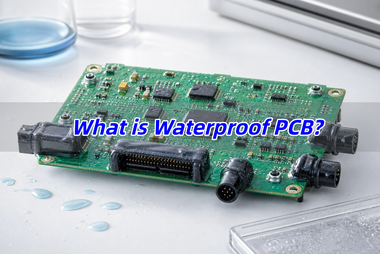
PCB manufacturing PCB manufacturing
Home > Blog

High Quality Rapid Prototyping PCB Assembly and Mass Production with Fast Turnaround

May 29th, 2026

Are you looking for rapid prototyping PCB assembly to accelerate product development while keeping costs and risks under control? Many companies use prototype assembly services to verify designs, test functionality, and prepare products for market launch before moving into larger production runs.

Rapid prototyping PCB assembly provides a faster and more flexible way to turn design files into working hardware. By validating a product before volume manufacturing, businesses can reduce delays, improve product quality, and transition to mass production with greater confidence.

Rapid Prototyping PCB Assembly, https://www.bestpcbs.com/blog/2026/05/rapid-prototyping-pcb-assembly/

What is Rapid Prototyping PCB Assembly?

Rapid prototyping PCB assembly is a manufacturing service designed to produce a small quantity of fully assembled PCBs within a short lead time. It allows businesses to transform design files into functional products for testing, evaluation, and validation before moving to larger production volumes.

Compared with traditional manufacturing, prototype assembly focuses on speed, flexibility, and quick feedback. It helps identify potential issues early, reducing the likelihood of costly changes during mass production.

A typical rapid prototype assembly service may include:

  • PCB fabrication and manufacturing
  • Electronic component sourcing
  • SMT and through-hole assembly
  • Inspection and testing procedures
  • Final assembly and shipment

The goal is to shorten development cycles, improve product readiness, and reduce manufacturing risks before full-scale production begins.

Why Choose Rapid Prototype PCB Assembly Before Mass Production?

Before investing in large production quantities, it is important to confirm that a design performs as expected. Prototype assembly provides an efficient way to evaluate functionality, manufacturability, and overall product readiness. Choosing prototype assembly before mass production offers several advantages:

  • Faster Product Validation – Verify performance and functionality using actual assembled hardware.
  • Lower Financial Risk – Avoid expensive production mistakes and unnecessary inventory costs.
  • Greater Design Flexibility – Implement design updates quickly without disrupting large manufacturing runs.
  • Better Production Planning – Identify sourcing, assembly, or manufacturing challenges before scaling production.
  • Improved Product Reliability – Resolve potential issues early and improve overall product quality.

When Should You Choose Rapid Prototype PCB Assembly?

Prototype assembly is not only for new designs. It is useful whenever a project requires testing, validation, demonstration, or small-volume production. Common situations include:

  • New Product Development – Validate new concepts before committing to larger production orders.
  • Functional Verification – Confirm that assembled PCBs operate according to design requirements.
  • Pilot Production Runs – Evaluate manufacturing readiness using a limited production quantity.
  • Product Demonstrations – Prepare working units for presentations, exhibitions, or market evaluations.
  • Design Improvement Cycles – Test revisions and enhancements before finalizing the design.
  • Low-Volume Market Launches – Support initial product releases while demand is being evaluated.

Rapid Prototyping PCB Assembly vs Mass Production: What is Difference?

Choosing between prototype assembly and mass production depends on your project’s stage, objectives, and timeline. While both services involve assembling PCBs, they differ significantly in production volume, lead time, flexibility, and overall manufacturing strategy.

Comparison ItemRapid Prototype PCB AssemblyMass Production PCB Assembly
Primary PurposeDesign validation and testingCommercial product manufacturing
Production Volume1–100 pcs (typically)Hundreds to millions of units
Lead Time24 hours to several daysSeveral weeks or months
Setup TimeMinimalLonger production preparation
Design ChangesEasy to implementDifficult and costly
Manufacturing FlexibilityVery highLimited
Initial InvestmentLowerHigher
Unit CostHigherLower
Risk LevelLower production riskHigher if design is unverified
Inventory CommitmentSmall quantityLarge inventory requirement
Component PurchasingSmall-volume sourcingBulk purchasing for lower costs
Time-to-MarketFasterSlower initial launch
Quality FocusDesign validation and functionalityProcess stability and consistency
Production EfficiencyLowerHigher
Supply Chain PlanningFlexible and adaptiveLong-term planning required
Testing PriorityProduct verificationProcess control and yield optimization
Production ScalingEasy transition to larger volumesAlready optimized for volume output
Suitable ProjectsNew products, pilot runs, design verificationMature products with stable demand
Cash Flow ImpactLower upfront investmentHigher upfront investment
Best Choice WhenProduct performance still needs validationProduct design has been fully approved
Rapid Prototyping PCB Assembly vs Mass Production, https://www.bestpcbs.com/blog/2026/05/rapid-prototyping-pcb-assembly/

How Does Rapid PCB Assembly Reduce Time-to-Market?

In today’s competitive market, launching a product earlier can create significant advantages. Faster development cycles allow businesses to receive feedback sooner, respond to market demand more quickly, and generate revenue earlier. Rapid PCB assembly helps shorten project timelines through several important benefits:

  • Shorter Development Cycles – Receive assembled PCBs quickly for testing and evaluation.
  • Faster Design Improvements – Identify issues early and implement updates without lengthy delays.
  • Reduced Waiting Time – Minimize the gap between design completion and hardware availability.
  • Earlier Production Planning – Begin sourcing and manufacturing preparation sooner.
  • Improved Project Scheduling – Keep development milestones on track and reduce unexpected delays.
  • Quicker Product Launches – Bring products to market faster and gain a competitive advantage.

Reducing time-to-market is not only about manufacturing speed. It is about improving efficiency throughout the entire product development process while maintaining quality and reliability.

What Factors Affect Rapid Prototyping PCB Assembly Lead Time?

Fast turnaround is one of the main reasons companies choose prototype assembly services. However, the total lead time is influenced by several factors throughout the manufacturing process, from material preparation to final delivery.

PCB Fabrication Requirements

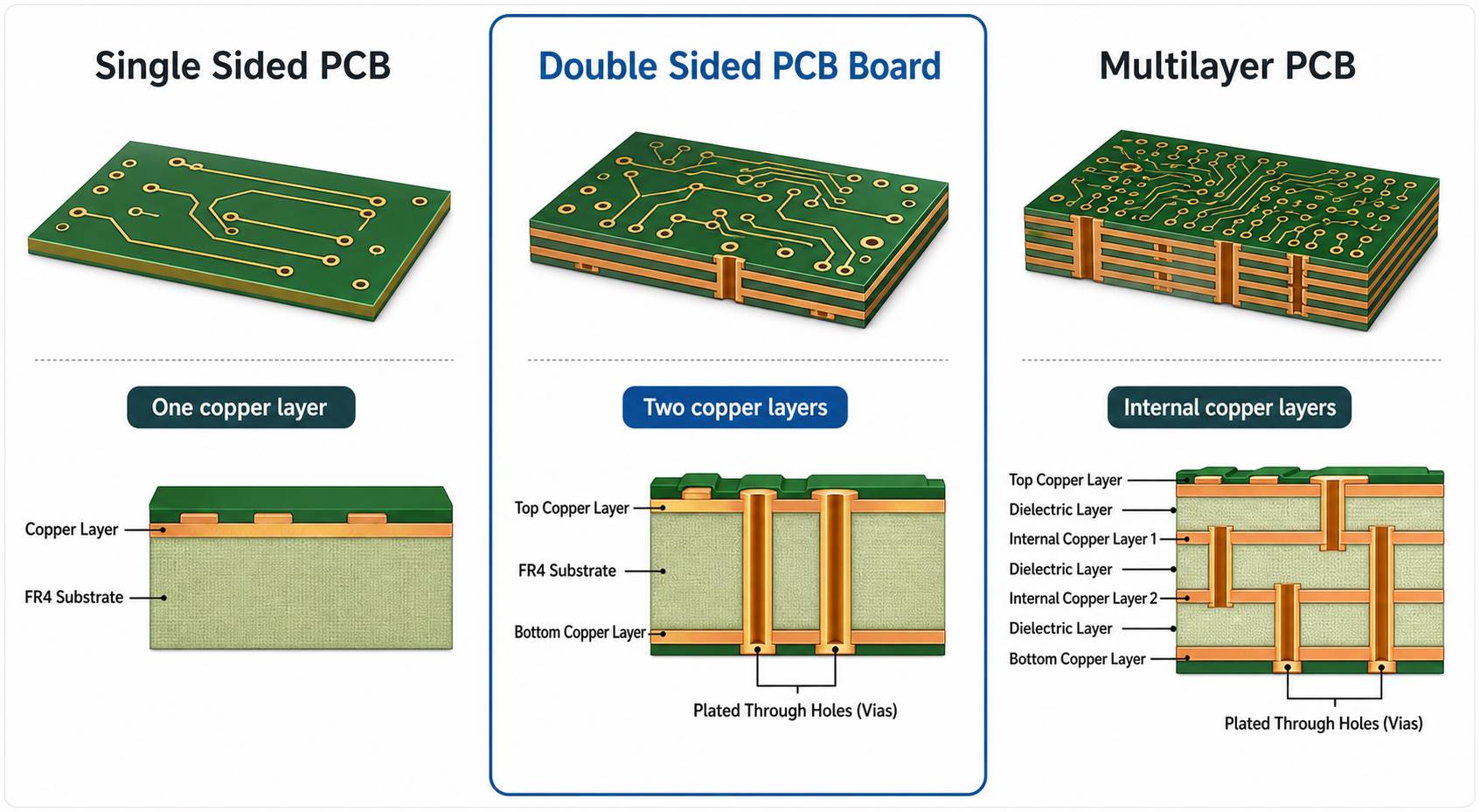
  • The PCB itself is often the first factor affecting delivery schedules. Standard PCBs can usually be manufactured quickly, while multilayer boards, high-frequency materials, metal-core PCBs, or special surface finishes may require additional production steps and processing time.

Component Availability

  • Component sourcing can have a significant impact on project timelines. If critical components are out of stock or have long procurement cycles, delivery schedules may be extended. Working with a supplier that has a stable supply chain can help reduce these risks.

Assembly Complexity

  • The number of components, package types, and assembly technologies all influence production time. Boards containing BGAs, fine-pitch devices, or mixed SMT and through-hole components generally require more setup, assembly, and inspection processes.

Testing and Inspection Requirements

  • Quality inspections such as AOI, X-ray inspection, and functional testing help ensure product reliability. Although these procedures require additional processing time, they significantly reduce the risk of defects during later development stages.

Order Quantity

  • Prototype projects typically involve smaller quantities and can often be completed quickly. As order volumes increase, assembly, inspection, and packaging requirements also increase.

Shipping Arrangements

  • Even after production is completed, logistics still affect the final delivery schedule. Choosing express shipping can help reduce overall turnaround time for urgent projects.
Rapid Prototyping PCB Assembly, https://www.bestpcbs.com/blog/2026/05/rapid-prototyping-pcb-assembly/

How Can We Ensure High Quality in Rapid Prototyping PCB Assembly?

A prototype is more than just a sample board. It is the foundation for future product development and volume production. For this reason, maintaining high quality throughout the assembly process is essential. At EBest, quality control begins before production starts and continues until the finished boards are ready for shipment.

Incoming Material Inspection

  • Every project starts with verifying the quality of incoming materials. Components and bare PCBs are inspected to ensure they meet production requirements before assembly begins.

Automated Optical Inspection (AOI)

  • AOI equipment is used to inspect component placement, polarity, solder joints, and other assembly details. This process helps identify potential defects early and improves overall assembly consistency.

X-Ray Inspection for Advanced Packages

  • For BGA components and hidden solder joints, X-ray inspection provides an additional level of verification. This helps ensure proper solder connections that cannot be checked through visual inspection alone.

Controlled Manufacturing Processes

  • Stable solder paste printing, accurate component placement, and controlled reflow profiles all contribute to consistent assembly quality. Process control helps reduce variation between boards.

Functional Testing

  • When required, assembled PCBs can undergo functional testing to confirm that they perform according to design expectations before shipment.

Final Quality Verification

  • Before delivery, finished assemblies undergo final inspection to verify workmanship, assembly accuracy, and overall product condition.

How Do We Ensure On-Time Delivery for Rapid Prototyping PCBA Orders?

For many projects, speed is just as important as quality. Delays in prototype delivery can affect testing schedules, product launches, and future production planning.

To support fast turnaround requirements, EBest focuses on efficient coordination across every stage of the manufacturing process.

Fast PCB Manufacturing Capability

  • With in-house PCB production resources and expedited manufacturing services, urgent PCB orders can often be processed much faster than traditional production schedules.

Stable Component Supply Chain

  • A strong global sourcing network helps improve component availability and reduce procurement-related delays. This is especially important when projects require multiple component types from different suppliers.

High-Speed SMT Production Lines

  • Modern assembly equipment enables efficient processing of both prototype and production orders. High placement capacity helps shorten manufacturing cycles and improve delivery performance.
Flexible Production Scheduling

  • Production resources can be adjusted according to project priorities, helping urgent orders move through manufacturing more efficiently.

Integrated Project Management

  • Coordinating PCB fabrication, component sourcing, assembly, testing, and shipping through one supplier helps eliminate communication delays and improves overall workflow efficiency.

Efficient Logistics Support

  • Reliable shipping partners and flexible transportation options help ensure products reach their destination on schedule.

Why Choose EBest for Rapid Prototyping PCB Assembly and Volume Production?

Selecting the right manufacturing partner can simplify product development, improve delivery performance, and reduce overall project risks. Beyond manufacturing capability, a reliable supplier should also provide flexibility, responsiveness, and long-term production support.

With more than 19 years of experience, EBest provides one-stop PCB and PCBA solutions for prototype and volume production projects worldwide.

One-Stop Manufacturing Services

  • PCB fabrication, component sourcing, assembly, testing, and box build services can all be managed through a single supplier. This reduces communication complexity and shortens project timelines.

Fast Turnaround Support

  • Urgent projects often require quick action. Our manufacturing capabilities allow prototype orders to move through production efficiently while maintaining quality standards.

Strong Component Sourcing Capability

  • A stable supply chain helps improve material availability and supports smoother project execution, especially for projects with demanding schedules.

Advanced Assembly Capability

  • We support SMT, through-hole assembly, mixed-technology assemblies, BGA packages, flex PCBs, ceramic PCBs, and many other specialized manufacturing requirements.

Prototype to Production Support

  • Projects can move seamlessly from prototype validation to full-scale manufacturing without changing suppliers, helping maintain consistency throughout the product lifecycle.

Certified Quality Systems

  • Our manufacturing processes are supported by internationally recognized certifications, including ISO 9001, IATF 16949, ISO 13485, AS9100D, RoHS, REACH, and UL.

Global Manufacturing Experience

  • Years of experience serving international markets allow us to support a wide range of industries and project requirements.
Rapid Prototyping PCB Assembly, https://www.bestpcbs.com/blog/2026/05/rapid-prototyping-pcb-assembly/

FAQs About Rapid Prototyping PCB Assembly Services

Q1: How fast can rapid prototyping PCB assembly be completed?

A1: The turnaround time depends on PCB complexity, component availability, assembly requirements, and testing needs. Standard prototype projects can often be completed within a few days, while urgent orders may be expedited to support tight development schedules. Working with a supplier that offers PCB fabrication, component sourcing, and assembly under one roof can further reduce lead times.

Q2: What files are required to get a PCB assembly quotation?

A2: To receive an accurate quotation, it is recommended to provide Gerber files, BOM lists, assembly drawings, and Pick & Place files if available. Complete project documentation helps eliminate unnecessary back-and-forth communication, improves quotation accuracy, and speeds up project evaluation.

Q3: Can you source electronic components for my project?

A3: Yes. We provide complete component sourcing services as part of our one-stop PCB assembly solution. A stable supply chain helps improve component availability, reduce procurement risks, and shorten overall project timelines. This allows projects to move into production more efficiently.

Q4: Can prototype PCB assembly be scaled to mass production later?

A4: Absolutely. Many products begin with prototype validation and later transition into volume production. Using the same manufacturing partner helps maintain consistent quality standards, sourcing channels, and production processes, making the transition smoother and more cost-effective.

Q5: What types of PCBs do you support for assembly?

A5: We support a wide range of PCB technologies, including FR4 PCBs, multilayer PCBs, metal core PCBs, ceramic PCBs, flex PCBs, rigid-flex PCBs, and high-frequency PCBs. This enables us to support projects across industrial, medical, automotive, communication, and consumer electronics applications.

Q6: How do you ensure the quality of prototype PCB assembly?

A6: Quality control is implemented throughout the manufacturing process. This includes incoming material inspection, AOI inspection, X-ray inspection for complex packages, process monitoring, functional testing, and final inspection before shipment. These procedures help improve reliability and reduce the risk of assembly defects.

Q7: Do you provide worldwide shipping services?

A7: Yes. We regularly ship PCB assembly orders to customers around the world. Multiple logistics options are available to support different delivery schedules and budget requirements, helping ensure products arrive safely and on time.

Get a Fast Quote for Your PCB Assembly Project

Whether you need prototype PCB assembly or volume production, EBest provides reliable, high-quality manufacturing services with fast turnaround. From PCB fabrication and component sourcing to assembly and testing, we help simplify the entire production process.

Simply send us your Gerber files, BOM list, and project requirements for a fast quotation. Contact EBest today to reduce lead times, improve product quality, and bring your products to market faster. Email: sales@bestpcbs.com.

You may also like

PCB on PCB Design: Stacking, Assembly and Testing

May 29th, 2026

PCB on PCB refers to a design where one printed circuit board is mounted, stacked, or electrically connected to another PCB. In practical electronics manufacturing, this structure is often called board-to-board PCB assembly, stacked PCB assembly, mezzanine PCB design, or PCB module integration. Engineers use it when one board cannot efficiently hold all functions, when a product needs replaceable modules, or when space is limited inside the enclosure.

This guide explains how PCB on PCB structures work, what interconnection methods are used, what design risks should be checked, and how manufacturers control quality during fabrication and assembly.

What Is PCB on PCB?

PCB on PCB is a construction method where two or more circuit boards are connected together through board-to-board connectors, pin headers, sockets, castellated holes, soldered pads, flex circuits, or custom interposers. One PCB may work as the main control board, while the second PCB may carry power, RF, sensors, displays, memory, communication modules, or daughter-card functions.

This design is common in compact electronic products because it allows engineers to separate circuit functions without expanding the main board area. For example, a product may use one base PCB for power and control, then place a smaller PCB above it for wireless communication or high-speed signal processing.

In manufacturing terms, PCB on PCB is not only a layout decision. It also affects connector selection, stack height, soldering process, mechanical tolerance, inspection access, repair strategy, and final functional testing.

PCB on PCB Design: Stacking, Assembly and Testing

Why Is PCB on PCB Important in Compact Electronics?

PCB on PCB is important because many modern electronic products require higher circuit density, modular design, and easier system upgrades. Instead of forcing every circuit into one crowded board, engineers can divide the system into several functional boards.

Design NeedHow PCB on PCB Helps
Limited enclosure spaceUses vertical space instead of increasing board length or width
Modular product architectureAllows separate communication, sensor, display, or power modules
Faster design updatesOne daughter board can be redesigned without changing the full system
Mixed technology integrationRF, analog, digital, and power circuits can be separated
Production flexibilityDifferent product versions can share the same main board

For products such as industrial controllers, medical electronics, IoT devices, handheld instruments, automotive modules, and communication equipment, PCB on PCB design can reduce layout congestion and improve product scalability.

How Does PCB on PCB Work?

A PCB on PCB structure works by creating electrical and mechanical connection between two boards. The connection method depends on signal type, current level, stack height, product size, vibration environment, and production volume.

The most common structure uses a main PCB and a daughter PCB. The two boards are connected by mating board-to-board connectors, pin headers, sockets, or solderable edge contacts. Board-to-board connectors are widely used because they allow PCBs to be connected without wire harnesses and support compact product structures.

A reliable PCB on PCB design must control three points:

Control PointEngineering Requirement
Electrical pathStable power, ground, signal, impedance, and current capacity
Mechanical alignmentCorrect connector position, mating height, board spacing, and tolerance
Assembly processReflow compatibility, inspection access, test points, and final verification

When these points are planned early, the stacked PCB assembly is easier to manufacture, inspect, and scale into production.

Main Types of PCB on PCB Structures

PCB on PCB structures can be designed in several ways. Each type has different benefits, cost levels, and assembly requirements.

TypeDescriptionCommon Use
Board-to-board connector stackTwo PCBs are connected by mating connectorsIndustrial control, IoT, medical electronics
Pin header and socket stackSimple vertical connection using through-hole or SMT headersPrototypes, control modules, display boards
Mezzanine PCBHigh-density board mounted above a main boardCommunication devices, embedded systems
Castellated moduleSmall PCB soldered directly onto another PCB edgeWireless modules, sensor modules
Flex-to-board connectionFlexible circuit links two rigid PCBsWearables, cameras, compact devices
Rigid-flex PCB alternativeRigid and flexible sections are fabricated as one structureHigh-reliability compact electronics
Soldered board-on-board moduleOne small PCB is directly soldered to pads on the main PCBRF modules, power modules, miniaturized devices

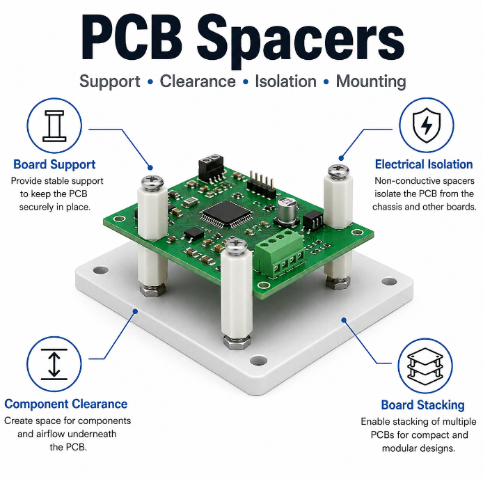
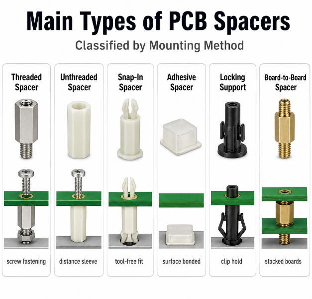
For low-cost applications, pin headers may be enough. For compact and high-reliability electronics, fine-pitch board-to-board connectors or castellated modules are often preferred. For high-vibration products, mechanical support should be added through screws, spacers, staking, or enclosure locking features.

PCB on PCB vs Single PCB Design

A single PCB is often simpler to fabricate and assemble. PCB on PCB becomes valuable when the product requires modularity, vertical space usage, mixed circuit separation, or easier design iteration.

ItemSingle PCBPCB on PCB
Board areaLarger footprint may be requiredUses vertical space efficiently
Assembly complexityUsually simplerRequires connector or module alignment
Design updatesWhole board may need revisionOne module can be updated separately
TestingOne complete board test flowBoard-level and system-level testing needed
CostLower for simple productsHigher if connectors and extra assembly are required
Repair or replacementMore difficult for single failed functionModule-level replacement may be possible
Signal controlEasier when routing is simpleRequires careful inter-board signal planning

For early engineering samples, PCB on PCB can shorten development when different functional modules need independent verification. For high-volume production, it should be evaluated carefully because connectors, assembly fixtures, tolerance control, and testing all affect total cost.

PCB on PCB vs Single PCB Design

Materials Used in PCB on PCB Manufacturing

The material selection depends on product environment, signal speed, heat, voltage, and mechanical stress.

MaterialTypical Use
FR4General control boards, power boards, communication modules
High-Tg FR4Products exposed to higher thermal stress
Rogers or other RF laminatesAntenna, RF, microwave, and high-frequency boards
Aluminum PCBLED, power, and thermal management modules
Copper base PCBHigh-power heat dissipation applications
Ceramic PCBHigh thermal conductivity, high power, RF, and harsh environments
Flexible polyimideCompact inter-board bending connection

In PCB on PCB design, both boards do not always need the same material. A main board may use FR4, while a daughter board may use Rogers material for RF performance or ceramic substrate for thermal control. This mixed-material strategy can improve performance without forcing the whole system to use expensive materials.

Key Design Rules for PCB on PCB Layout

PCB on PCB layout should start with mechanical planning, not only circuit routing. The connector location, board spacing, enclosure clearance, and assembly sequence should be confirmed before final placement.

Design ItemWhat to Check
Connector footprintMatch supplier land pattern and orientation
Stack heightConfirm board-to-board distance after mating
Board outlineAvoid enclosure interference and component collision
Keep-out areaReserve space around connectors, screws, and tall components
Signal assignmentPlace high-speed, power, ground, and low-speed pins logically
Ground return pathProvide enough ground pins near high-speed signals
Test accessKeep test points reachable after stacking
Thermal pathAvoid trapping heat between boards
Mechanical supportAdd spacers, screws, or brackets for vibration-prone products
Assembly directionMake sure the board can be soldered, inspected, and mated correctly

For high-speed PCB on PCB designs, impedance control and return-path continuity are especially important. The PCB stack-up should define copper layers, dielectric thickness, material type, controlled impedance values, and ground reference planes before routing starts.

Board-to-Board Connectors for PCB on PCB Assembly

Board-to-board connectors are one of the most widely used solutions for PCB on PCB products. They support different orientations, spacing requirements, pin counts, and electrical needs. Some connector families are designed for high-speed signals, while others are optimized for power transfer, floating alignment, or compact stacking.

When choosing a connector, engineers should compare:

ParameterSelection Point
PitchSmaller pitch saves space but increases assembly difficulty
Stack heightMust match enclosure and component clearance
Current ratingMust support power rail requirements
Voltage ratingMust meet product safety and insulation needs
Mating cyclesImportant for removable or serviceable modules
Alignment toleranceFloating connectors help absorb small mechanical offsets
Contact platingGold plating improves contact reliability in many signal applications
SMT or through-holeSMT saves space; through-hole improves mechanical strength
Signal speedHigh-speed connectors need controlled impedance performance
AvailabilityLong-term supply and second-source risk should be reviewed

A common mistake is selecting a connector only by pin count. In production, mating height, coplanarity, pick-and-place compatibility, reflow profile, and inspection method are just as important.

Manufacturing Process for PCB on PCB Products

PCB on PCB manufacturing normally involves both PCB fabrication and PCBA assembly. The exact process depends on whether the boards are detachable, soldered together, or assembled as a complete electronic module.

A typical process includes:

StepProcess Detail
DFM reviewCheck board outline, connector footprint, solder mask, drill design, and assembly clearance
PCB fabricationProduce each board according to stack-up, copper weight, surface finish, and tolerance requirements
Incoming inspectionVerify PCB dimensions, finish, solder mask, and electrical test status
SMT assemblyPlace components and board-to-board connectors using stencil printing and reflow soldering
Through-hole assemblyAdd pin headers, sockets, spacers, or mechanical supports when required
Board cleaningRemove flux residue when the product requires high cleanliness
Sub-assembly testTest each PCB before final stacking where possible
Final matingJoin boards using connectors, soldering, screws, or fixtures
Functional testVerify full system performance after all boards are connected
Packing and traceabilityRecord batch data, inspection results, and shipment information

IPC-A-610 provides acceptance requirements for electronic assemblies, while IPC-J-STD-001 covers requirements for soldered electrical and electronic assemblies. These standards are often referenced in PCB assembly quality control.

Testing Methods for PCB on PCB Assembly

Testing is critical because faults may appear at the board level, connector level, or full-system level. A PCB may pass electrical testing as a bare board, then fail after stacking because of connector alignment, solder joint defects, signal integrity problems, or mechanical stress.

Test MethodPurpose
Bare board electrical testCheck open and short circuits before assembly
AOIInspect component placement, polarity, solder joints, and visible defects
X-ray inspectionInspect hidden solder joints, BGA, QFN, and some connector solder areas
Flying probe testVerify assembled circuits without expensive fixtures
ICTCheck component values, shorts, opens, and node-level faults
Functional testConfirm product operation under real working conditions
Power-on testCheck current draw, voltage rails, and startup behavior
Connector mating testConfirm stable electrical contact after board stacking
Thermal testCheck heat concentration between stacked boards
Vibration or drop testUsed when the product faces mechanical stress

For high-reliability products, test planning should be done before layout completion. Test points must remain accessible after the boards are stacked. If the daughter board blocks key signals, the manufacturer may need custom fixtures, pogo-pin access, boundary scan, or staged testing.

Quality Standards and Compliance for PCB on PCB

PCB on PCB products may need different standards depending on the final application. For bare rigid printed boards, IPC-6012 covers qualification and performance requirements for rigid PCBs, including single-sided, double-sided, multilayer, blind or buried via, and metal core boards.

For visual acceptability of bare boards, IPC-A-600 describes target, acceptable, and nonconforming conditions that can be externally or internally observed on printed boards.

For environmental compliance, RoHS restricts hazardous substances in electrical and electronic equipment in the European Union. For safety-related PCB requirements, UL provides PCB testing and certification services against UL standards and other international, national, and regional requirements.

DocumentWhy It Matters
Gerber filesDefine copper, solder mask, silkscreen, and routing layers
Drill filesDefine plated and non-plated holes
IPC-356 netlistHelps verify electrical connectivity
BOMDefines components, connectors, alternatives, and sourcing rules
Pick-and-place fileSupports automated SMT assembly
Assembly drawingShows component position, polarity, and stacking direction
Stack-up drawingDefines material, copper, dielectric, and impedance structure
Test specificationDefines inspection and functional test requirements
Quality standard requirementClarifies IPC class, RoHS, UL, or customer-specific rules

Common Failure Modes in PCB on PCB Designs

PCB on PCB failure often comes from mechanical, electrical, or process-related mismatch. Many issues can be prevented during DFM review.

Failure ModePossible CausePrevention Method
Intermittent signalConnector misalignment or weak contactUse correct mating height, alignment posts, and mechanical support
Cracked solder jointsBoard flexing, vibration, or heavy connector stressAdd screws, spacers, strain relief, or stronger connector type
Poor RF performanceLong return path or wrong connector assignmentPlace ground pins near RF or high-speed signals
OverheatingHeat trapped between stacked boardsAdd thermal vias, copper area, airflow gap, or heat sink path
Assembly collisionTall components placed between boardsRun 3D mechanical clearance check
Solder bridgingFine-pitch connector footprint or stencil issueOptimize stencil aperture and solder paste volume
Hard-to-test boardTest points blocked after stackingAdd staged test points and fixture access early
Connector sourcing riskSingle-source connector selectedCheck lifecycle, MOQ, lead time, and approved alternatives

A strong engineering approach is to treat the connector area as both an electrical interface and a mechanical load point. This helps reduce field failures caused by repeated plugging, vibration, thermal cycling, or enclosure pressure.

Applications Using PCB on PCB

PCB on PCB structures are used in many electronic products where compact design, modularity, and multi-function integration are required.

ApplicationTypical PCB on PCB Function
Industrial controlMain control board plus I/O, relay, or communication module
Medical electronicsSensor board, display board, control board, or power module
Automotive electronicsLED driver module, radar board, control module, or interface board
IoT devicesWireless module mounted on a base control PCB
Communication equipmentRF board stacked with digital processing board
RoboticsMotor control board connected to sensor or communication board
Consumer electronicsDisplay, camera, charging, or button module
Aerospace and UAVLightweight modular electronics with compact interconnects
Test instrumentsReplaceable measurement boards and interface modules
LED lightingPower driver board connected with control or thermal board

For RF and high-speed applications, PCB on PCB design should be reviewed carefully because connector transition, grounding, impedance discontinuity, and board spacing can affect signal performance.
Case Study: Custom PCB on PCB Manufacturing for an Industrial Control Module

A customer needed a compact industrial control module with power regulation, signal processing, and communication functions inside a limited enclosure. A single PCB layout created routing congestion and made thermal separation difficult. The engineering solution was to use a PCB on PCB structure.

The lower board handled power input, protection circuits, and I/O terminals. The upper daughter board carried the microcontroller, communication interface, and signal conditioning circuits. Board-to-board connectors were selected based on stack height, current rating, and available mating tolerance.
During DFM review, the connector footprint was checked against the supplier datasheet. Tall capacitors were moved away from the stacking area. Test points were placed on the board edges so the assembly could be tested before and after final mating. Mechanical spacers were added to reduce connector stress during installation.

The production flow included PCB fabrication, SMT assembly, AOI inspection, sub-board testing, final board stacking, functional test, and packing with batch traceability. This approach reduced layout pressure, improved module organization, and made future product upgrades easier.

Cost Factors in PCB on PCB Manufacturing

PCB on PCB cost is affected by both PCB fabrication and assembly complexity. The cheapest structure is not always the most economical after testing, rework, and reliability risks are considered.

Main cost factors include:

Cost FactorImpact
Number of boardsMore boards increase fabrication, assembly, and inspection steps
Connector typeFine-pitch, high-speed, floating, or high-current connectors cost more
Stack height toleranceTight mechanical tolerance may require higher-grade connectors or fixtures
PCB materialRF, ceramic, aluminum, copper base, and high-Tg materials affect cost
Surface finishENIG is common for fine-pitch connectors and reliable contact areas
Assembly difficultyFine-pitch connectors, double-sided SMT, and hidden joints increase process control needs
Test fixtureStacked products may require custom functional test fixtures
Production volumeHigher volume can reduce unit assembly cost after fixture investment
Quality requirementsIPC class, traceability, inspection depth, and documentation affect total cost
Component sourcingLong lead-time connectors or single-source parts can increase procurement cost

For cost control, engineers should confirm whether the product needs a detachable PCB module or a permanently soldered module. A removable connector improves serviceability but may cost more. A soldered castellated module can save height and connector cost, but it changes the repair and inspection strategy.

How to Choose a PCB on PCB Manufacturer

A reliable PCB on PCB manufacturer should understand both PCB fabrication and PCBA assembly. This matters because inter-board products require control across layout review, board tolerance, connector assembly, soldering, inspection, testing, and final system verification.

Before placing an order, check whether the manufacturer can provide:

CapabilityWhat to Confirm
DFM reviewConnector footprint, stack height, solderability, test access, and mechanical clearance
PCB fabricationMultilayer PCB, impedance control, HDI, RF PCB, MCPCB, ceramic PCB, or rigid-flex capability
PCBA assemblySMT, through-hole, mixed assembly, fine-pitch connector placement, and reflow control
Component sourcingBoard-to-board connector availability, approved alternatives, and lifecycle checking
TestingAOI, X-ray, electrical test, ICT, flying probe, and functional test
Quality systemIPC workmanship, RoHS support, traceability, and inspection records
Engineering supportBOM review, stack-up suggestions, assembly fixture advice, and failure analysis
Global deliveryExport packing, shipment coordination, and batch documentation

For OEM and ODM projects, the manufacturer should also help evaluate whether the PCB on PCB structure is the best solution compared with one larger PCB, rigid-flex PCB, cable connection, or integrated module design.

What Files Are Needed Before Quoting PCB on PCB?

A complete quotation package helps the manufacturer evaluate cost, process, and risk accurately.

Prepare these files before requesting a quote:

File or InformationRequirement
Gerber filesRequired for each PCB
Drill filesInclude plated and non-plated hole information
BOMInclude manufacturer part number, quantity, tolerance, package, and alternatives
Pick-and-place fileRequired for SMT assembly
Assembly drawingShow connector direction, polarity, and board stacking relationship
Stack-up requirementInclude material, copper thickness, board thickness, and impedance
3D modelStrongly recommended for stacked board clearance checking
Test planDefine electrical, functional, and environmental test requirements
Annual volumeHelps select suitable process and sourcing strategy
Compliance requirementRoHS, UL, IPC class, medical, automotive, aerospace, or customer-specific rules

For connector-based designs, the connector datasheet should also be provided. The mating pair, stack height, orientation, and tolerance must be checked before production.

FAQs About PCB on PCB

Q1: What does PCB on PCB mean?

PCB on PCB means one printed circuit board is mounted, stacked, soldered, or connected to another PCB. It is often used for daughter boards, communication modules, sensor modules, RF modules, display boards, and compact electronic assemblies. The purpose is usually to save space, separate functions, or make the product easier to upgrade.

Q2: Is PCB on PCB the same as board-to-board PCB assembly?

They are closely related. Board-to-board PCB assembly is one common form of PCB on PCB design. It usually uses connectors, headers, sockets, or direct soldering to connect two PCBs. PCB on PCB is a broader phrase because it can also include castellated modules, mezzanine boards, flex-linked boards, or soldered PCB modules.

Q3: What connector is best for PCB on PCB design?

The best connector depends on pitch, stack height, current rating, signal speed, vibration level, and mating cycle requirement. For simple control boards, pin headers may be enough. For compact industrial or medical devices, fine-pitch board-to-board connectors are often better. For vibration environments, floating or mechanically reinforced connectors are worth reviewing.

Q4: Can PCB on PCB be used for high-speed signals?

Yes, but the layout must control impedance, grounding, connector transition, and return path. High-speed signals should be assigned near ground pins, and the connector should support the required data rate. The PCB stack-up, connector datasheet, and signal integrity requirements should be reviewed together before layout approval.

Q5: Can one PCB be soldered directly onto another PCB?

Yes. A small module can be soldered directly onto a main board through castellated holes, edge pads, or solderable terminals. This method saves connector height and cost, but it makes rework more difficult. It is commonly used for wireless modules, compact sensors, and small functional modules.

Q6: Is PCB on PCB better than using cables?

PCB on PCB is often better when the product needs compact size, stable alignment, and reduced wire harness complexity. Cables are still useful when boards need flexible movement or longer spacing. The better option depends on enclosure design, vibration, assembly process, signal type, and maintenance needs.

Q7: What is the biggest risk in PCB on PCB assembly?

The biggest risk is usually poor coordination between mechanical design, connector selection, and assembly process. If stack height, component clearance, and connector tolerance are not checked early, the boards may collide, misalign, or create unstable contact. A 3D model and DFM review can prevent most of these problems.

Q8: Which surface finish is suitable for PCB on PCB?

ENIG is commonly used for fine-pitch assembly, flat soldering surfaces, and contact reliability. HASL may be acceptable for some low-cost boards, but it is less ideal for fine-pitch connector pads because of surface unevenness. The final choice depends on connector pitch, soldering process, cost target, and product reliability level.

Q9: How should PCB on PCB products be tested?

Testing should be done in stages. Each bare PCB should receive electrical testing first. After SMT assembly, AOI, X-ray, flying probe, or ICT may be used. After final stacking, functional testing should verify power, signal communication, connector contact, current draw, and product behavior under normal operating conditions.

Q10: Does PCB on PCB increase manufacturing cost?

It can increase cost because there are multiple boards, connectors, assembly steps, and test requirements. However, it may reduce redesign cost, enclosure size, wiring labor, and future upgrade cost. For modular products, the overall project cost may be better than forcing all functions into one complex PCB.

Q11: What spacing is needed between two stacked PCBs?

The spacing depends on connector height, tallest components, insulation clearance, airflow, and enclosure requirements. Engineers should check the connector mated height, component maximum height, solder joint profile, and manufacturing tolerance. A 3D clearance review is recommended before ordering prototypes.

Q12: Can PCB on PCB be used in automotive or medical electronics?

Yes. It can be used in automotive, medical, industrial, aerospace, and communication products when design, material, process, and testing requirements are properly controlled. For regulated industries, documentation, traceability, inspection standards, reliability testing, and supplier qualification become more important than in simple consumer products.

Conclusion

PCB on PCB design is a practical solution for compact, modular, and function-rich electronic products. It allows engineers to divide circuits into main boards and daughter boards, reduce layout congestion, and support different materials or technologies inside one product. The best result depends on early connector selection, stack-height planning, signal integrity review, test access, and manufacturing process control.

For selection, start with product structure and signal requirements. Then compare board-to-board connectors, soldered modules, flex connections, and rigid-flex alternatives. For purchasing, provide complete Gerber files, BOM, assembly drawings, stack-up data, connector datasheets, and test requirements so the manufacturer can review cost and production risk accurately.

If you are looking for reliable OEM manufacturing, ODM production, sample development, mass production, or custom engineering solutions, contact our engineering team for technical support and quotation service.


You may also like

Solder Paste Stencil Printing Process & Design Guide

May 29th, 2026

Are you choosing a solder paste stencil and wondering which specifications matter most for SMT assembly? A solder paste stencil controls solder paste deposition on PCB pads, helping improve printing accuracy, solder joint consistency, and overall assembly quality.

This guide explains stencil materials, thickness options, design guidelines, printing methods, cleaning procedures, and service life. Whether for prototypes or volume production, understanding these fundamentals can help achieve more reliable SMT results.

Solder Paste Stencil, https://www.bestpcbs.com/blog/2026/05/solder-paste-stencil/

What is Solder Paste Stencil?

A solder paste stencil is a thin metal sheet with precisely cut openings that match the pad layout on a PCB. During SMT assembly, solder paste is printed through these openings onto specific locations before component placement.

Most stencils are manufactured from stainless steel using laser-cut technology. The openings determine how much solder paste is deposited on each pad, making stencil accuracy critical to assembly quality.

The stencil acts as a template between the PCB and the printing process. Without controlled solder deposition, issues such as solder bridging, insufficient solder, or poor solder joints may occur during reflow.

Because of its ability to deliver consistent solder volume and repeatable printing results, the stencil has become a standard tool in modern SMT manufacturing.

What is a Stencil Used for Solder Pasting?

The main purpose of a stencil is to transfer a controlled amount of solder paste onto PCB pads before component placement. Each aperture is designed according to the size and shape of the corresponding pad.

A stencil helps ensure that every solder joint receives a similar volume of paste. This consistency is important for achieving stable reflow results and reducing assembly defects.

During printing, a squeegee pushes solder paste across the stencil surface. The paste fills the apertures and is transferred onto the PCB when the stencil separates from the board.

Compared with manual dispensing, stencil printing offers higher efficiency, better repeatability, and more uniform solder paste deposition, making it suitable for both prototypes and volume production.

What Materials Are Used for Solder Paste Stencils?

The most common materials used for solder paste stencils are stainless steel, electroformed nickel, and nano-coated stainless steel. Among them, stainless steel is the most widely used because it offers a good balance of durability, printing performance, and cost.

Stainless steel stencils are suitable for most SMT assembly applications and can withstand thousands of printing cycles. They are commonly used in both prototype and mass production.

For fine-pitch components and high-density PCB designs, electroformed nickel stencils provide smoother aperture walls and better solder paste release performance.
Some manufacturers also use nano-coated stencils, which reduce solder paste adhesion and improve cleaning efficiency during continuous production.

MaterialMain AdvantageTypical Use
Stainless SteelDurable and economicalGeneral SMT assembly
Electroformed NickelBetter paste releaseFine-pitch devices
Nano-Coated StencilCleaner printingHigh-volume production

What is the Thickness of Solder Paste Stencil?

The standard solder paste stencil thickness is typically 0.08 mm, 0.10 mm, 0.12 mm, 0.15 mm, and 0.20 mm. For most SMT assemblies, 0.10 mm and 0.12 mm are the most commonly used options.

Thinner stencils are generally selected for fine-pitch components and high-density PCB layouts because they provide better control of solder paste volume and help reduce bridging.

Thicker stencils are often used for connectors, power devices, and components that require a larger amount of solder during assembly.

Stencil ThicknessTypical Applications
0.08 mm0201, 0402, fine-pitch ICs
0.10 mmMixed SMT assemblies
0.12 mmStandard SMT production
0.15 mmLarge components and connectors
0.20 mmHigh solder volume requirements
Solder Paste Stencil, https://www.bestpcbs.com/blog/2026/05/solder-paste-stencil/

Solder Paste Stencil Design Guidelines

Proper stencil design directly affects solder paste transfer, solder joint quality, and SMT production yield. A well-designed stencil helps achieve consistent printing results while reducing common assembly defects.

  • Match stencil thickness to component size. Fine-pitch ICs and miniature components usually require thinner stencils, while connectors and power devices often need thicker stencils to provide sufficient solder volume.
  • Optimize aperture size instead of copying pad dimensions exactly. In many cases, reducing the aperture slightly improves solder paste release and lowers the risk of solder bridging.
  • Maintain a proper area ratio. The stencil area ratio affects how easily solder paste releases from the aperture. An area ratio greater than 0.66 is generally recommended for stable printing performance.
  • Use window-pane openings for large thermal pads. Dividing a large aperture into multiple smaller openings helps distribute solder more evenly and reduces voiding during reflow.
  • Modify apertures for fine-pitch components. BGAs, QFNs, and fine-pitch ICs may require reduced or specially shaped apertures to improve printing accuracy and minimize solder defects.
  • Consider spacing between adjacent pads. Components with tight pad spacing are more prone to solder bridging, so aperture design should be adjusted accordingly.
  • Ensure smooth aperture walls. Laser-cut and polished apertures improve solder paste release and help maintain consistent print quality over long production runs.
  • Review manufacturing tolerances before fabrication. Verify aperture dimensions, pad alignment, and solder volume requirements to ensure the stencil can be manufactured accurately.

What Equipment Is Used for Solder Paste Stencil Printing?

Accurate solder paste printing requires several pieces of equipment working together. Each tool contributes to alignment accuracy, solder paste control, and process consistency.

  • Stencil Printer – Aligns the PCB and stencil before printing. Automatic printers provide higher throughput and better consistency than manual systems.
  • Squeegee Blade – Pushes solder paste across the stencil surface and fills the apertures. Blade pressure, speed, and angle directly affect print quality.
  • PCB Support System – Uses support fixtures or vacuum platforms to keep the PCB flat during printing and prevent movement.
  • Vision Alignment System – Uses cameras to align stencil apertures with PCB pads before printing begins.
  • Solder Paste Inspection (SPI) System – Measures solder paste volume, height, and coverage to identify printing defects before component placement.
  • Stencil Cleaning System – Removes residual solder paste from stencil surfaces and apertures, helping maintain stable printing performance.
How to Make a Solder Paste Stencil?

A solder paste stencil is usually manufactured from PCB Gerber files and serves as the foundation of the SMT printing process. A well-made stencil helps ensure accurate solder paste deposition, while a poorly designed stencil can lead to solder bridging, insufficient solder, or inconsistent printing results.
  • Prepare the solder paste layer data. The stencil manufacturer uses the PCB solder paste layer to generate aperture openings. Before production, verify pad sizes, component spacing, and special package requirements.
  • Optimize aperture openings. Apertures are often adjusted rather than copied directly from PCB pads. Small reductions can improve solder paste release and help prevent excess solder deposition.
  • Choose the correct stencil thickness. Thickness should match component density and solder volume requirements. Fine-pitch assemblies generally require thinner stencils, while connectors and power devices may require thicker stencils.
  • Laser cut the stencil. Laser cutting is the most widely used manufacturing method because it offers excellent dimensional accuracy and consistent aperture quality.
  • Electropolish the apertures. Polishing smooths the aperture walls and improves solder paste release, especially for fine-pitch components.
  • Perform final inspection. Aperture dimensions, stencil flatness, and overall quality should be verified before the stencil enters production.

How to Frame a Solder Paste Stencil?

Framing ensures that the stencil remains flat and properly tensioned during printing. Proper installation is important because even a small alignment error can affect solder paste deposition accuracy.

  • Select the appropriate frame type. Framed stencils are commonly used for continuous production, while frameless stencils are often preferred for prototypes and small-volume orders.
  • Inspect the stencil before installation. Check for scratches, bending, contamination, or other damage that may affect print quality.
  • Mount the stencil evenly. Uniform tension across the stencil surface helps prevent distortion during printing.
  • Verify alignment references. Fiducials and positioning marks should remain visible and accurately positioned after framing.
  • Run a trial print. Testing before production helps identify alignment issues and confirms that solder paste deposits are forming correctly.

How to Apply Solder Paste with Stencil?

Stencil printing is the most common method used in SMT manufacturing because it provides fast, accurate, and repeatable solder paste deposition. Consistent printing is essential for achieving reliable solder joints during reflow.

  • Secure the PCB firmly. The board should be supported properly to prevent movement during printing.
  • Align the stencil accurately. Apertures must match PCB pads precisely to ensure solder paste is deposited in the correct locations.
  • Apply the correct amount of solder paste. Too little paste can cause weak joints, while excessive paste increases the risk of bridging.
  • Use proper squeegee settings. Squeegee pressure, speed, and angle should remain consistent throughout production.
  • Separate the stencil smoothly. Careful separation helps maintain clean solder paste deposits and prevents smearing.
  • Inspect the printed result. Check solder paste height, shape, and coverage before component placement.
Solder Paste Stencil, https://www.bestpcbs.com/blog/2026/05/solder-paste-stencil/

How to Clean Solder Paste Stencil?

Cleaning is an important part of stencil maintenance. Residual solder paste left inside apertures can affect paste release and eventually lead to printing defects.

  • Clean the stencil regularly during production. Frequent cleaning helps prevent aperture blockage and maintains stable print quality.
  • Use compatible cleaning solutions. Cleaning chemicals should remove solder paste effectively without damaging the stencil surface.
  • Pay special attention to fine-pitch apertures. Small openings are more likely to trap solder paste and require thorough cleaning.
  • Inspect the stencil during maintenance. Cleaning provides an opportunity to identify scratches, wear, or damaged apertures.
  • Store the stencil correctly after cleaning. Proper storage helps prevent contamination and mechanical damage.

What is Solder Paste Stencil Life?

A high-quality solder paste stencil can typically be used for thousands to tens of thousands of printing cycles under normal production conditions. The actual lifespan depends on stencil material, printing frequency, and maintenance practices.

Regular cleaning helps maintain solder paste release performance and extends stencil life. Residual solder paste inside apertures can affect printing accuracy and lead to inconsistent solder deposition.

Proper storage is also important. Stencils should be protected from bending, scratches, and contamination to maintain printing precision.

A stencil should be replaced when aperture wear, deformation, or poor paste release begins affecting print quality. A well-maintained stencil helps ensure consistent solder paste deposition and reliable SMT production results.

How to Apply Solder Paste without Stencil?

Although stencil printing is preferred for most SMT assemblies, manual solder paste application can be useful for prototypes, repairs, and very small production runs.

  • Use a dispensing syringe. This is the most common alternative method and allows solder paste to be placed directly onto individual pads.
  • Choose a suitable dispensing tip. Smaller tips provide better control when working with miniature components.
  • Apply solder paste carefully. Excessive paste may cause solder bridging, while insufficient paste can affect solder joint strength.
  • Inspect the paste deposits before assembly. Checking placement accuracy helps reduce defects during reflow.
  • Reserve this method for low-volume work. Manual application is flexible but generally cannot match the consistency and efficiency of stencil printing.

For prototype projects, manual application can be effective, but for production quantities a stencil remains the most reliable solution.

Solder Paste Stencil, https://www.bestpcbs.com/blog/2026/05/solder-paste-stencil/

FAQs About Solder Paste Stencils

Q1: What is the HS Code for Solder Paste Stencils?

A1: The HS code varies by country and customs regulations. Solder paste stencils are commonly classified as industrial metal templates or SMT manufacturing tools. Always confirm the exact code with your customs broker before shipment.

Q2: What is the Difference Between Framed and Frameless Stencils?

A2: Framed stencils include a fixed aluminum frame, while frameless stencils require a reusable mounting system. Framed stencils are preferred for production runs, while frameless stencils are more economical for prototypes and small batches.

Q3: Do I Need a Stencil for Solder Paste?

A3: No, but a stencil is the most accurate and efficient way to apply solder paste. Manual application is suitable for prototypes and repairs, while stencil printing provides better consistency and higher production efficiency.

Q4: Which Stencil Thickness Is Best for Fine-Pitch Components?

A4: A thickness of 0.08 mm to 0.10 mm is commonly used for fine-pitch components. Thinner stencils provide better control of solder volume and help reduce solder bridging.

Q5: When Should a Solder Paste Stencil Be Replaced?

A6: A stencil should be replaced when wear, damage, or poor paste release affects print quality. Replacing worn stencils helps maintain consistent solder deposition and SMT yield

Conclusion

A well-designed solder paste stencil helps ensure accurate solder paste deposition, reliable solder joints, and stable SMT assembly results. Choosing the right stencil specifications and maintaining proper printing practices can significantly improve production quality and efficiency.

If you are looking for a reliable SMT assembly partner, EBest PCB provides one-stop SMT services, including SMT stencil fabrication, component sourcing, SMT assembly, THT assembly, testing, and final product assembly. Whether you need prototypes or volume production, our team is ready to support your project with fast turnaround and dependable quality. Contact sales@bestpcbs.com today for a quotation.

You may also like

Top 10 Flexible Circuit Board Suppliers for Medical Devices

May 29th, 2026

Finding the right flexible circuit board suppliers for medical devices is not only about price. Medical electronics usually require compact design, stable quality, clean documentation, and reliable assembly support.

Flexible circuits are used in wearable monitors, hearing aids, diagnostic tools, imaging systems, catheter systems, and portable medical devices. This guide helps you quickly compare board types, design points, manufacturing capabilities, certifications, and supplier options. For project review or medical PCB assembly quotes, you can also send your Gerber files and BOM to sales@bestpcbs.com.

Flexible Circuit Board Suppliers for Medical Devices

What Are Flexible Circuit Boards for Medical Devices?

Flexible circuit boards are PCBs made with bendable materials, usually polyimide. They can fold, bend, or fit into small spaces where standard rigid PCBs are not practical.

For medical devices, flexible circuits help reduce wiring, save space, and improve internal structure. They are often used to connect sensors, displays, batteries, buttons, antennas, and control modules.

TypeTypical Use
Single-sided flex circuitsSimple medical interconnection
Double-sided flex circuitsMore routing space
Multilayer flex circuitsHigher signal density
Rigid flex circuit boardsCompact medical device structures
Custom etched flex circuitsSensor and special connection designs

Why Medical Flex Circuits Are Used in Medical Electronics?

Medical flex circuits are used because medical products are becoming smaller, lighter, and more integrated.

They help engineers:

  • Reduce cables and connectors
  • Save internal space
  • Improve assembly layout
  • Support curved or compact housings
  • Connect multiple functional areas
  • Build lightweight medical electronics

In many medical devices, the circuit must fit the product shape. That is where flex circuits and rigid-flex boards become practical.

What Types of Flexible Circuit Boards Are Used in Medical Devices?

EBest Circuit (Best Technology) supports several flexible PCB types for medical electronics projects.

Board TypeApplication Fit
Single-sided flexible circuitsSimple signal connection
Double-sided flexible circuitsMedium-density routing
Multilayer flexible circuitsCompact medical modules
Rigid flex circuit boardsIntegrated rigid + flexible structure
Custom flexible PCBDevice-specific mechanical design
Custom etched flex circuitsSensor, electrode, and special circuit paths
Flexible PCB with stiffenerConnector or SMT support
Medical PCB assembliesFabrication + component assembly

These board types are suitable for wearable devices, portable diagnostic equipment, handheld instruments, monitoring devices, and compact medical control modules.

Medical Device PCB Design: PCB Layout Guidelines for Flexible Circuits

Medical device PCB design should start from the product structure, not only the schematic.

Design AreaWhat to Check
Bend radiusAvoid sharp bending in flex areas
Trace routingUse smooth routing in bending zones
Component placementKeep parts away from active flex areas
ViasAvoid vias in repeated bending areas
Stiffener locationSupport connectors and SMT areas
GroundingImprove signal stability
ShieldingProtect sensitive medical signals
DFM reviewCheck manufacturability before production

For rigid flex circuit boards, the transition area between rigid and flex sections is especially important. Poor layout in this area can affect yield and reliability.

Custom Flexible PCB and Medical PCB Assembly Manufacturing Capabilities

EBest Circuit (Best Technology) provides comprehensive end-to-end solutions, from custom flexible PCB​ fabrication and rigid flex circuit boards​ integration to precision medical device PCB assembly services. Our operations are engineered specifically to meet the stringent reliability, miniaturization, and regulatory demands of the healthcare industry.

Core Capabilities in Medical-Grde Flex Circuits

As experts in medical flex circuits, we utilize advanced custom etched flex circuits​ technology to ensure superior performance:

  • Material Mastery:​ We utilize medical-grade polyimide (PI) and LCP substrates, ensuring full compliance with ISO 13485 and RoHS standards.
  • Precision Fabrication:​ Our capabilities include fine-line trace routing and micro-via technology, perfect for the compact medical device PCB design​ required in modern implants and wearables.
  • Rigid-Flex Solutions:​ We seamlessly integrate flex circuits​ with rigid sections, providing 3D packaging solutions that reduce weight and improve signal integrity for critical medical electronics.

Excellence in Medical PCB Assembly

Being a trusted medical PCB manufacturer​ means we never compromise on quality. Our medical PCB assembly​ processes are designed for zero-defect outcomes:

  • Advanced Assembly:​ We offer high-precision SMT, BGA/CSP placement, and medical electronics assembly​ with sterilization-resistant coatings.
  • Quality Assurance:​ Our medical PCB assembly services​ include 100% AOI/X-ray inspection and functional testing, aligning with FDA and GMP requirements.
  • Full-System Integration:​ From prototype to volume production of medical PCB assemblies, we manage the entire lifecycle, including box-build integration.

Ready to start your next medical electronic assembly project? Just feel free to contact EBest Circuit (Best Technology)​ at sales@bestpcbs.com​ for expert support with your custom flexible PCB​ and medical PCB assemblies.

Certifications for Medical PCB Manufacturing and Assembly

Certifications help customers screen medical PCB suppliers faster.

Certification / StandardWhy It Matters
ISO 9001General quality management
ISO 13485Medical device quality management
IPC standardsPCB fabrication and assembly workmanship
RoHS / REACHMaterial compliance for global markets
UL materialsRequired for some product designs

For high-reliability medical electronics, IPC Class 3 is often discussed during flex PCB manufacturing review.

Medical Applications Using Rigid Flex Circuit Boards

Rigid flex circuit boards are used when a medical device needs both mechanical support and flexible connection.

ApplicationWhy Rigid-Flex Helps
Wearable monitorsThin, light, body-friendly structure
Hearing aidsCompact curved internal layout
EndoscopesNarrow and flexible circuit path
Catheter systemsLong, thin, flexible connection
Portable diagnostic toolsReduced cables and smaller housing
Imaging equipmentStable signal routing
Surgical instrumentsCompact and durable internal design
Patient monitoring devicesIntegrated sensor and control connection

Case Study: EBest Circuit (Best Technology) Manufacturing Medical Flex Circuits

Project Type:
2-layer medical FPC for compact medical electronics.

Customer Requirement:
The customer needed a thin, flexible circuit with steel stiffeners on both sides for better assembly support.

EBest Circuit (Best Technology) Support:

  • Reviewed FPC stack-up and material structure
  • Checked coverlay opening and solder mask design
  • Controlled steel stiffener alignment
  • Used ENIG finish for stable solderability
  • Added white silkscreen markings for UL 94 V-0 and RoHS
  • Controlled bonding with 0.025mm pure thermal adhesive

Manufacturing Focus:
Thin FPC structure, stiffener bonding, flatness control, coverlay registration, and final surface quality.

Board Parameters

ItemSpecification
Board Type2-layer FPC
Board Thickness0.16mm ±0.03mm
Copper Type1/2 oz ED Cu
Base Material1 mil adhesive PI
Coverlay1 mil yellow coverlay
Surface FinishENIG 2U”
Solder MaskGreen solder mask
SilkscreenWhite silkscreen
Compliance MarkingUL 94 V-0, RoHS
Top Stiffener0.2mm steel stiffener
Bottom Stiffener0.2mm steel stiffener
Stiffener Adhesive0.025mm pure thermal adhesive
Key Control PointsStiffener alignment, bonding strength, flatness, coverlay registration

Top 10 Flexible Circuit Board Suppliers for Medical Devices

Below are 10 suppliers commonly found when researching medical flex circuits, rigid-flex PCBs, and medical PCB assembly services.

Company NameCertificationsKey Capabilities
EBest Circuit (Best Technology)ISO 9001, ISO 13485, UL, RoHSMedical flex circuits, rigid-flex PCB, medical PCB assembly, DFM review
Epec Engineered TechnologiesISO, UL, IPCMedical flex PCB, rigid-flex PCB, reliability testing
FralockISO 13485, ISO 9001, AS9100D, FDA registeredFlex circuits, rigid-flex, stiffeners, shielding, turnkey builds
BENCORISO 9001, ULFlexible PCB, rigid-flex PCB, design, fabrication, assembly
Rush PCBISO 9001, ISO 13485, UL, RoHS/REACHFlex PCB, rigid-flex PCB, medical PCB assembly, quick-turn service
All Flex SolutionsAS9100, ISO 9001, ESD S20.20Flexible circuits, CatheterFlex, rigid-flex, medical device PCBs
MincoISO 9001, AS9100D, NadcapHigh-reliability flex circuits, rigid-flex, multilayer flex
Cirexx InternationalISO 9001, AS9100, ITAR, IPCFlex PCB, rigid-flex PCB, layout, fabrication, assembly
Flex Plus FPCISO 9001, ISO 13485, IATF 16949, ULMedical FPC, hearing aid FPC, portable monitor FPC
HT Medical DevicesISO 13485, FDA registered product buildsFlexible circuits, rigid-flex, catheter flex, endoscope flex

Before choosing a supplier, compare certifications, flex PCB capability, assembly support, traceability, quote speed, and engineering communication.

How to Choose Flexible Circuit Board Suppliers for Medical Devices

Use this checklist before sending a medical PCB project to a supplier:

CheckpointWhy It Matters
Medical PCB experienceReduces communication risk
Flex and rigid-flex capabilitySupports more device structures
ISO 13485Important for medical supply chains
DFM supportFinds layout issues early
SMT assemblySaves supplier coordination time
Component sourcingSupports one-stop medical electronics assembly
Testing capabilityImproves delivery confidence
TraceabilityHelps audits and production records
Fast RFQ responseSpeeds up project evaluation

A strong supplier should not only quote. They should review your files and point out manufacturing risks.

Future Trends of Custom Flexible PCB for Medical Devices

Custom flexible PCB will continue to grow in medical electronics because devices are getting smaller and more wearable.

Key trends include:

  • More wearable medical monitors
  • More rigid-flex designs in compact devices
  • Smaller sensor modules
  • Higher-density routing
  • Better signal shielding
  • Stronger traceability requirements
  • More demand for one-stop PCB + assembly service
  • Earlier DFM review before production

For medical device developers, this means the PCB supplier should join the project earlier, not only after the design is finished.

FAQs About Flexible Circuit Board Suppliers for Medical Devices

Q1. What are flexible circuit board suppliers for medical devices?
They are PCB manufacturers that provide flex circuits, rigid-flex boards, and sometimes medical PCB assembly for medical electronics.

Q2. What are medical flex circuits used for?
They are used in wearable monitors, hearing aids, diagnostic devices, imaging systems, catheter systems, and compact medical electronics.

Q3. What is the difference between flex circuits and rigid flex circuit boards?
Flex circuits are bendable boards. Rigid flex circuit boards combine rigid PCB areas and flexible connection areas in one design.

Q4. Can custom flexible PCB be used in wearable medical devices?
Yes. It helps reduce size, weight, and wiring inside wearable medical products.

Q5. What files are needed for medical PCB assembly quotes?
Usually Gerber files, BOM, pick-and-place file, assembly drawing, testing requirements, quantity, and material requirements.

Q6. What should be checked in medical device PCB design?
Bend radius, trace routing, stiffener position, connector support, component placement, surface finish, and DFM feedback.

Q7. Why is ISO 13485 important?
It shows the supplier has a medical device quality management system.

Q8. Can flexible circuits support SMT assembly?
Yes. Components are usually mounted on rigid or reinforced areas to improve assembly stability.

Q9. What affects medical PCB assembly cost?
Layer count, material, size, copper thickness, surface finish, components, assembly difficulty, testing, and order quantity.

Q10. Does EBest Circuit (Best Technology) provide medical PCB assembly services?
Yes. EBest Circuit (Best Technology) supports flex PCB fabrication, rigid-flex PCB manufacturing, component sourcing, SMT assembly, DFM review, testing, and medical PCB assembly services.

In conclusion, choosing flexible circuit board suppliers for medical devices should be based on capability, quality control, medical experience, and engineering support.

EBest Circuit (Best Technology) provides custom flexible PCB, rigid flex circuit boards, medical flex circuits, medical PCB assembly, DFM review, component sourcing, and testing support. Pls feel free to send your Gerber files, BOM, drawings, and project requirements to sales@bestpcbs.com for a medical PCB assembly quote.

You may also like

PCB Coating

May 29th, 2026

PCB coatings are protective layers applied to printed circuit board assemblies to improve reliability in demanding environments. They help protect electronic components, solder joints, and conductive traces from moisture, corrosion, dust, chemicals, salt spray, vibration, and temperature changes.

Choosing the right PCB coating type is important for product lifespan, electrical safety, field reliability, and long-term cost control. This guide explains the main coating materials, how they work, where they are used, how they compare, and what buyers should check before placing an order.

What Are PCB Coating Types?

PCB coating types refer to different protective materials used to cover printed circuit boards after assembly. These coatings form a thin insulating barrier over exposed conductive areas while allowing the circuit to function normally.

What Are PCB Coating Types

The most common PCB coating types include acrylic coating, silicone coating, polyurethane coating, epoxy coating, Parylene coating, and nano coating. Each coating has different strengths in moisture resistance, chemical resistance, temperature resistance, flexibility, repairability, and cost.

Why Are PCB Coatings Important?

Electronic assemblies can fail when moisture, dust, chemical residues, salt ions, or conductive contamination reach the PCB surface. These conditions may cause corrosion, leakage current, insulation degradation, dendrite growth, and short circuits.

PCB coatings help improve reliability by reducing environmental damage and protecting sensitive circuits during long-term operation.

  • Protect copper traces and solder joints from corrosion
  • Improve insulation resistance
  • Reduce leakage current
  • Prevent moisture-related failures
  • Improve reliability in harsh environments
  • Extend product service life
  • Reduce maintenance and warranty costs

How Do PCB Coatings Work?

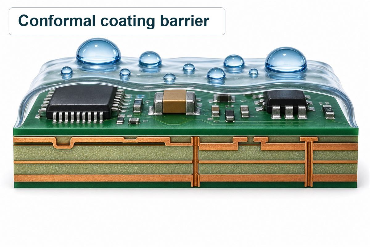
PCB coatings work by creating a physical and electrical barrier between the circuit board and the external environment. This barrier blocks or reduces the contact between conductive surfaces and moisture, oxygen, chemicals, dust, and salt contamination.

Protection FunctionPurpose
Moisture ProtectionPrevents water vapor from reaching conductive surfaces
Corrosion ProtectionIsolates metal surfaces from oxygen and contaminants
Electrical InsulationReduces leakage current and improves dielectric performance
Chemical ResistanceProtects against solvents, oils, fuels, and industrial chemicals
Mechanical ProtectionReduces damage caused by vibration, shock, and handling
Thermal StabilityMaintains coating performance during temperature cycling

What Types of PCB Coatings Are Available?

Acrylic Coatings

Acrylic coatings are widely used because they are cost-effective, easy to apply, and easy to repair. They provide good moisture protection for general electronic products and are suitable for many commercial and industrial applications.

Advantages:

  • Low cost
  • Fast drying
  • Easy inspection
  • Excellent reworkability
  • Good moisture resistance

Limitations:

  • Moderate chemical resistance
  • Limited high-temperature performance
  • Lower durability than polyurethane or Parylene coating
Acrylic Coatings

Common applications: consumer electronics, communication equipment, control boards, and indoor industrial electronics.

Silicone Coatings

Silicone coatings offer excellent flexibility and strong performance under high temperature, low temperature, humidity, and vibration. They are commonly used in outdoor electronics and automotive applications.

Advantages:

  • Excellent thermal stability
  • Good flexibility
  • Strong humidity resistance
  • Good vibration resistance
  • Suitable for thermal cycling environments

Limitations:

  • Higher cost than acrylic coating
  • More difficult to remove for repair

Common applications: automotive electronics, LED lighting, outdoor equipment, renewable energy systems, and power modules.

Polyurethane Coatings

Polyurethane coatings provide strong resistance to moisture, solvents, chemicals, abrasion, and salt spray. They are suitable for harsh industrial and marine environments where corrosion risk is high.

Advantages:

  • Excellent chemical resistance
  • Strong moisture barrier
  • Good abrasion resistance
  • Good salt spray protection

Limitations:

  • Difficult rework
  • Longer curing time

Common applications: industrial automation, marine electronics, oil and gas equipment, and chemical processing systems.

Epoxy Coatings

Epoxy coatings create a hard and durable protective layer with strong adhesion and high mechanical strength. They are often used when the PCB requires strong physical protection and chemical resistance.

Advantages:

  • High mechanical strength
  • Strong adhesion
  • Excellent chemical resistance
  • Durable protection

Limitations:

  • Limited flexibility
  • Difficult to remove or repair
  • May not be suitable for components exposed to high mechanical stress from thermal expansion

Common applications: power electronics, industrial control systems, heavy-duty equipment, and high-reliability modules.

Parylene Coatings

Parylene coating is applied through a chemical vapor deposition process under vacuum conditions. It forms a highly uniform, thin, and pinhole-free protective layer, even around complex geometries and small component gaps.

Advantages:

  • Uniform coverage
  • Pinhole-free protection
  • Extremely low moisture vapor transmission rate
  • Excellent dielectric properties
  • Outstanding corrosion protection

Limitations:

  • Higher processing cost
  • Specialized equipment required
  • Difficult rework

Common applications: medical devices, aerospace electronics, defense systems, sensors, and high-reliability electronic assemblies.

Nano Coatings

Nano coatings create an ultra-thin hydrophobic layer on the PCB surface. They are mainly used for lightweight moisture protection in compact electronics where coating thickness must be minimized.

Advantages:

  • Very thin coating layer
  • Lightweight protection
  • Minimal effect on component dimensions
  • Good water-repellent performance

Limitations:

  • Lower protection than Parylene coating
  • Limited performance in extreme industrial environments

Common applications: smartphones, wearable devices, portable electronics, and consumer electronic products.

What Materials Are Used in PCB Coatings?

The coating material determines the protection level, repairability, curing process, and long-term reliability of the PCB assembly.

MaterialKey CharacteristicTypical Use
Acrylic ResinCost-effective and easy to repairGeneral electronics
Silicone PolymerFlexible and thermally stableAutomotive and outdoor electronics
Polyurethane ResinStrong chemical resistanceIndustrial and marine electronics
Epoxy ResinHigh mechanical strengthPower and heavy-duty electronics
Poly-Para-XylyleneUniform vapor-deposited protectionMedical, aerospace, and defense electronics
Nano PolymersUltra-thin hydrophobic protectionCompact consumer electronics

What Are the Advantages of PCB Coatings?

PCB coatings provide multiple reliability benefits for electronic products used in demanding environments.

  • Improved moisture resistance
  • Better corrosion protection
  • Enhanced electrical insulation
  • Reduced risk of short circuits
  • Improved protection against dust and contamination
  • Longer service life
  • Higher field reliability

For many industrial, automotive, medical, and outdoor applications, coating is an important process for reducing failure risk and improving product stability.

What Are the Limitations of PCB Coatings?

PCB coatings improve protection, but they also introduce additional manufacturing and design considerations.

  • Additional material and processing cost
  • Longer production cycle
  • Possible repair difficulty
  • Masking requirements for connectors and test points
  • Inspection complexity
  • Compatibility concerns with certain components or materials

The best coating choice should balance protection level, application environment, cost, production volume, and maintenance requirements.

How Do Different PCB Coatings Compare?

Coating TypeMoisture ProtectionChemical ResistanceTemperature ResistanceReworkability
AcrylicGoodModerateModerateExcellent
SiliconeExcellentGoodExcellentModerate
PolyurethaneExcellentExcellentGoodDifficult
EpoxyExcellentExcellentVery GoodVery Difficult
ParyleneOutstandingOutstandingExcellentDifficult
NanoModerateModerateGoodGood

How Do You Choose the Right PCB Coating?

The right PCB protective coating depends on the actual operating environment and product reliability target. A coating that works well for consumer electronics may not be suitable for automotive, marine, aerospace, or medical applications.

Key selection factors include:

  • Operating temperature range
  • Humidity exposure
  • Salt spray exposure
  • Chemical exposure
  • UV exposure
  • Vibration and mechanical stress
  • Repair and rework requirements
  • Required coating thickness
  • Compliance standards
  • Total project budget

Which Industries Use PCB Coatings?

PCB coatings are widely used in industries where electronic reliability is critical.

Automotive Electronics

Automotive PCB assemblies must withstand temperature cycling, vibration, humidity, and road salt. Common applications include engine control units, battery management systems, ADAS modules, lighting control systems, and power distribution modules.

Industrial Automation

Industrial control boards are often exposed to dust, oil mist, vibration, humidity, and electrical noise. PCB coatings help protect PLC controllers, sensors, motor drives, robotics systems, and power control modules.

Medical Devices

Medical electronics require high reliability, stable insulation, and clean protection. Parylene coating is often used in medical devices because it provides uniform barrier protection and strong dielectric performance.

Aerospace and Defense

Aerospace and defense electronics require long-term reliability under harsh operating conditions. Coatings are used in flight control systems, radar equipment, satellite electronics, navigation systems, and communication modules.

Renewable Energy

Solar inverters, wind turbine controllers, and energy storage systems often operate in outdoor or semi-outdoor environments. PCB coatings help reduce moisture damage and corrosion risk.

What Design Considerations Are Important Before Applying PCB Coating?

PCB coating should be considered during the design stage, not only after assembly. Proper design planning can reduce coating defects and make production easier.

  • Define areas that require masking
  • Keep connectors and test points accessible
  • Check component spacing and coating flow
  • Review thermal dissipation requirements
  • Confirm material compatibility
  • Consider future repair needs
  • Avoid trapping residues under the coating

What Manufacturing Methods Are Used for PCB Coating?

Spray Coating

Spray coating is suitable for medium- and high-volume production. It provides efficient coverage and can be automated for better consistency.

Dip Coating

Dip coating provides broad coverage by immersing the PCB assembly into coating material. It is effective for simple board designs but may produce thicker coating layers.

Selective Coating

Selective coating uses automated equipment to apply coating only to required areas. It improves precision, reduces masking work, and helps control material usage.

Brush Coating

Brush coating is commonly used for prototypes, repairs, and small production runs. It is flexible but less consistent than automated coating methods.

Chemical Vapor Deposition

Chemical vapor deposition is used for Parylene coating. It provides highly uniform protection and can cover complex shapes, edges, and small gaps.

What Industry Standards Apply to PCB Coatings?

Industry standards help define coating material performance, inspection requirements, and assembly quality expectations.

IPC-CC-830

IPC-CC-830 defines qualification and performance requirements for conformal coating materials used on electronic assemblies.

IPC-A-610

IPC-A-610 provides acceptance criteria for electronic assemblies, including workmanship and inspection requirements.

UL Certification

UL certification helps evaluate material safety, flammability, and electrical performance for specific applications.

RoHS Compliance

RoHS compliance restricts hazardous substances in electronic products and is important for products sold into many global markets.

REACH Compliance

REACH regulates chemical substances used in manufacturing and supports safer material selection for international supply chains.

How Are PCB Coatings Tested?

Testing helps verify whether the coating has been applied correctly and whether it can meet the expected reliability requirements.

  • Visual inspection
  • UV fluorescence inspection
  • Coating thickness measurement
  • Adhesion testing
  • Salt spray testing
  • Thermal cycling testing
  • Humidity testing
  • Insulation resistance testing

What Are the Most Common PCB Coating Failures?

Common PCB coating failures are usually related to poor cleaning, incorrect coating thickness, improper curing, or weak process control.

  • Delamination
  • Cracking
  • Blistering
  • Pinholes
  • Poor adhesion
  • Incomplete coverage
  • Contamination trapped under the coating

Many coating failures can be prevented through proper cleaning, controlled application parameters, validated curing conditions, and regular inspection.

How Can PCB Coating Defects Be Prevented?

Defect prevention starts before the coating process. The PCB assembly should be clean, dry, and compatible with the selected coating material.

  • Use proper cleaning before coating
  • Control humidity and temperature during application
  • Validate coating thickness
  • Use correct curing conditions
  • Mask connectors and contact areas carefully
  • Inspect boards under UV light when applicable
  • Record process parameters for traceability

What Factors Affect PCB Coating Costs?

PCB coating cost depends on the coating material, process method, board complexity, production quantity, masking requirements, and testing specifications.

  • Coating material type
  • PCB size and layout complexity
  • Coating thickness
  • Production volume
  • Application method
  • Masking difficulty
  • Inspection and testing requirements
  • Certification requirements

Acrylic coating is usually more economical, while Parylene coating generally has higher processing costs because it requires specialized vacuum deposition equipment.

How Can Buyers Ensure PCB Coating Quality?

Buyers should not evaluate coating quality only by price. A reliable PCB coating supplier should provide stable process control, material traceability, inspection capability, and engineering support.

  • Confirm coating material specifications
  • Check IPC and compliance requirements
  • Review inspection methods
  • Ask for coating thickness control capability
  • Confirm masking and process requirements
  • Check production traceability
  • Evaluate supplier experience with similar applications

How Do You Choose a Reliable PCB Coating Supplier?

A reliable PCB coating supplier should understand both the coating process and the final application environment. This is especially important for automotive, industrial, medical, aerospace, and outdoor electronic products.

  • Experience with different PCB coating types
  • Engineering support for material selection
  • Stable coating and curing process
  • Inspection and testing capability
  • Quality documentation and traceability
  • Prototype and mass production support
  • Global delivery experience

What Should Be Checked Before Placing a PCB Coating Order?

Before placing an order, buyers should clearly define the technical and quality requirements. This helps reduce misunderstanding and prevents delays during production.

  • Application environment
  • Coating material type
  • Required coating thickness
  • Masking areas
  • Testing standards
  • Documentation requirements
  • Lead time
  • Packaging requirements

Frequently Asked Questions About PCB Coating Types

What is the most commonly used PCB coating?

Acrylic coating is one of the most commonly used PCB coatings because it is cost-effective, easy to apply, and easy to rework. It is suitable for many commercial and general industrial electronics.

Which PCB coating provides the best moisture protection?

Parylene coating usually provides the strongest moisture protection because it forms a uniform, pinhole-free barrier with very low moisture vapor transmission. Silicone and polyurethane coatings also perform well in humid environments.

Is Parylene better than silicone coating?

Parylene provides better barrier protection and uniform coverage, while silicone offers better flexibility and thermal cycling performance. The better choice depends on the operating environment and reliability requirement.

Which coating is recommended for outdoor electronics?

Silicone coating is often recommended for outdoor electronics because it performs well under temperature changes, humidity, UV exposure, and vibration. For more demanding environments, polyurethane or Parylene may be considered.

Can PCB coatings extend product lifespan?

Yes. PCB coatings can extend product lifespan by reducing moisture damage, corrosion, contamination, leakage current, and electrical failure risk. Proper coating selection can improve long-term reliability.

How thick should a PCB coating be?

Most conformal coatings are applied within a controlled thickness range based on material type and application requirements. The correct thickness should meet the required protection level without affecting connectors, heat dissipation, or repairability.

Are PCB coatings repairable?

Some PCB coatings are easier to repair than others. Acrylic coating is generally the easiest to remove and rework, while epoxy and Parylene coatings are more difficult to repair.

Which coating is best for automotive electronics?

Silicone coating is frequently used in automotive electronics because it provides strong temperature resistance, flexibility, and vibration protection. Polyurethane may also be used when chemical or salt spray exposure is important.

What standards should PCB coatings comply with?

Common standards and compliance requirements include IPC-CC-830, IPC-A-610, UL certification, RoHS, and REACH. The exact requirement depends on the product application and target market.

What causes PCB coating failure?

PCB coating failure is often caused by poor cleaning, trapped contamination, incorrect curing, excessive thickness, poor adhesion, or unsuitable coating selection. Stable process control is essential for preventing failures.

Conclusion

PCB coating types play an important role in improving the reliability, durability, and service life of electronic assemblies. Acrylic, silicone, polyurethane, epoxy, Parylene, and nano coatings each provide different levels of moisture protection, chemical resistance, temperature resistance, flexibility, and repairability.

For general electronics, acrylic coating offers a practical balance of cost and protection. For automotive and outdoor applications, silicone coating is often preferred because of its flexibility and thermal stability. For industrial, marine, medical, aerospace, and high-reliability applications, polyurethane, epoxy, or Parylene coating may provide stronger protection.

When selecting a PCB coating, engineers and buyers should evaluate the application environment, coating material, quality standards, inspection requirements, repair needs, and total lifecycle cost. A reliable supplier can help choose the most suitable PCB protective coating and provide stable production quality from prototype to mass production.

If you are looking for reliable OEM manufacturing, ODM production, prototype development, mass production, or custom engineering solutions, please contact our engineering team for technical support and quotation services.

You may also like

PCB Epoxy Resin Explained: Types, Applications and Removal Methods

May 29th, 2026

What is PCB epoxy, and why is it used in so many electronic products? From FR-4 substrates and protective coatings to encapsulation compounds and adhesives, PCB epoxy plays a critical role in improving electrical insulation, mechanical stability, and environmental resistance.

Because different epoxy materials are designed for different applications, understanding their properties and performance is essential. In this guide, you’ll learn about the main types of PCB epoxy, their performance characteristics, common applications, and factors that affect long-term PCB reliability.

PCB Epoxy, https://www.bestpcbs.com/blog/2026/05/pcb-epoxy/

What is Epoxy in PCB?

Epoxy is a thermosetting polymer widely used throughout PCB manufacturing and assembly processes. Once cured, it forms a durable material that provides electrical insulation, mechanical support, and environmental protection.

The most common example is FR-4, where epoxy resin is combined with fiberglass cloth to create a rigid substrate capable of supporting copper circuitry while maintaining excellent insulation properties.

In addition to PCB substrates, epoxy is also used as an adhesive, coating, encapsulation compound, and staking material. These applications help protect assemblies from moisture, vibration, dust, and chemicals.

Because of its excellent insulation, adhesion, and durability, epoxy remains one of the most important materials used in modern PCB manufacturing.

Why Use Epoxy on PCB?

Uppercase PCB needs stable structural protection and electrical insulation support in production and service. PCB epoxy is the most mainstream auxiliary material to meet these demands. It can solve common problems such as circuit short circuit, structural looseness and environmental corrosion in PCB operation, and improve the overall stability of circuit boards. Here are reasons why use epoxy on PCB:

  • Excellent insulation performance: Cured PCB epoxy forms a dense insulating layer on PCB surfaces and gaps. It effectively isolates circuits and prevents short circuit faults caused by circuit contact. It also avoids current leakage and ensures safe operation of electronic circuits.
  • Strong structural bonding effect: This material can bond copper foil, glass fiber substrates and electronic components firmly. It fixes loose parts of the PCB and enhances the overall structural firmness. It is widely used in pcb epoxy staking and internal lamination processes.
  • Effective environmental protection: Cured epoxy layer resists moisture, dust, acid and alkali corrosion. It isolates external humid and corrosive air from the PCB internal circuit. It greatly extends the service life of finished circuit boards.
  • Good shock and wear resistance: The cured epoxy colloid has certain toughness and hardness. It can buffer external vibration and impact force, and reduce component wear and falling off. It protects PCB circuits in complex working conditions.

What Kind of Epoxy for PCB Board?

Different epoxy products are used in PCB manufacturing and assembly depending on the application. Some are designed for structural bonding, while others focus on protection, insulation, thermal management, or component reinforcement. Selecting the appropriate epoxy helps improve reliability and manufacturing consistency.

Epoxy Adhesives

Epoxy adhesives are commonly used to bond components, heat sinks, connectors, and mechanical parts to a PCB. They provide strong adhesion, excellent durability, and good resistance to temperature and vibration.

Epoxy Encapsulation Compounds

PCB encapsulation epoxy completely surrounds electronic assemblies to protect them from moisture, dust, chemicals, and mechanical damage. This type of epoxy is widely used in industrial, automotive, and outdoor electronic products.

Potting Epoxy

Potting compounds fill cavities or enclosures around electronic assemblies. Compared with thin coatings, potting provides a higher level of environmental protection and mechanical support.

Epoxy Coatings

Epoxy PCB coating materials create a protective barrier on the PCB surface. They help prevent corrosion, contamination, and moisture-related failures while improving long-term reliability.

Staking Epoxy

PCB epoxy staking is used to secure large or vibration-sensitive components such as transformers, inductors, connectors, and capacitors. It helps prevent movement and reduces stress on solder joints.

Thermally Conductive Epoxy

This type of epoxy contains thermally conductive fillers that improve heat transfer. It is commonly used in LED modules, power electronics, and high-power assemblies where temperature management is important.

Conductive Epoxy

Conductive epoxy contains metallic particles that allow electrical conductivity after curing. It is sometimes used as an alternative to solder for specialized interconnection applications.

PCB epoxy type, https://www.bestpcbs.com/blog/2026/05/pcb-epoxy/

What Performance Parameters Do PCB Epoxy Have?

The performance parameters of PCB epoxy resin are listed below. These indicators directly determine the insulation capability, heat resistance, structural stability and overall service life of finished circuit boards, so they are essential references for material evaluation.

ParameterTypical Value / Range
Glass Transition Temperature (Tg)120°C – 250°C
Thermal Conductivity0.2 – 8.0 W/m·K
Dielectric Constant (Dk @ 1GHz)3.0 – 5.0
Dissipation Factor (Df @ 1GHz)0.002 – 0.030
Volume Resistivity10¹³ – 10¹⁶ Ω·cm
Surface Resistivity10¹² – 10¹⁵ Ω
Dielectric Strength15 – 35 kV/mm
Moisture Absorption0.05% – 1.00%
CTE (X-Y Direction)10 – 25 ppm/°C
CTE (Z Direction)40 – 250 ppm/°C
Tensile Strength40 – 100 MPa
Flexural Strength80 – 180 MPa
Compressive Strength100 – 250 MPa
Adhesion Strength10 – 35 MPa
HardnessShore D 75 – 95
Viscosity500 – 100,000 cP
Cure Temperature25°C – 180°C
Cure Time5 Minutes – 24 Hours
Operating Temperature-55°C to +200°C
Thermal Decomposition Temperature (Td)280°C – 400°C
UL Flammability RatingUL94 V-0 / V-1 / V-2
Cure Shrinkage0.1% – 2.0%
Water ResistanceExcellent
Chemical ResistanceGood to Excellent

What Are the Common Applications of Epoxy in PCB Manufacturing?

Epoxy materials are used throughout PCB fabrication and assembly.

FR-4 Laminate Production

  • Forms the base PCB structure
  • Bonds fiberglass layers together
  • Provides electrical insulation

PCB Encapsulation

  • Protects circuits from moisture
  • Improves environmental resistance
  • Extends service life

PCB Epoxy Staking

  • Secures heavy components
  • Improves vibration resistance
  • Reduces mechanical stress

Epoxy PCB Coating

  • Protects traces and solder joints
  • Prevents corrosion
  • Improves durability

Thermal Management

  • Transfers heat from components
  • Improves temperature control
  • Supports power electronics

Epoxy Ink PCB Screen Printing

  • Creates legends and markings
  • Improves identification
  • Supports manufacturing processes
PCB epoxy application, https://www.bestpcbs.com/blog/2026/05/pcb-epoxy/

How Does Epoxy Affect PCB Performance and Reliability?

Epoxy is more than just a protective material. It directly influences electrical performance, thermal stability, mechanical durability, and environmental resistance. Choosing the right epoxy can significantly improve the reliability and lifespan of a PCB assembly.

Improves Electrical Insulation

Epoxy creates an insulating barrier between conductive traces and components. High insulation resistance helps prevent electrical leakage, short circuits, and signal interference, especially in humid or contaminated environments.

Enhances Mechanical Stability

PCB assemblies are often exposed to vibration, impact, and thermal expansion. Epoxy helps secure components, distribute mechanical stress, and reduce the risk of cracked solder joints or component movement during operation.

Increases Resistance to Moisture and Chemicals

Moisture is one of the most common causes of PCB failure. Epoxy coatings and encapsulation materials help prevent water ingress, corrosion, oxidation, and chemical contamination, improving long-term reliability in harsh environments.

Supports Thermal Reliability

Temperature fluctuations cause materials to expand and contract at different rates. Properly selected epoxy materials help reduce thermal stress, minimize delamination risks, and improve stability during repeated heating and cooling cycles.

Protects Against Environmental Damage

Dust, salt spray, industrial pollutants, and other contaminants can gradually degrade electronic assemblies. Epoxy provides an additional protective layer that helps maintain performance in challenging operating conditions.

Extends Service Life

By improving insulation, strengthening mechanical support, enhancing environmental protection, and reducing thermal stress, epoxy contributes directly to longer product life and lower failure rates throughout the operating lifecycle.

How to Remove Epoxy Coating from PCB?

Removing epoxy from a PCB can be challenging because epoxy is designed to create a strong and durable bond. The removal method depends on the epoxy type, coating thickness, and whether the PCB needs to remain functional after the process. Careful removal helps minimize damage to copper traces, solder joints, and electronic components.

Identify the Type of Epoxy

Before starting, determine whether the material is a conformal coating, staking adhesive, encapsulation compound, or potting resin. Thin epoxy coatings are generally easier to remove than fully encapsulated assemblies.

Use Controlled Heat for Softening

Many epoxy materials become softer when exposed to moderate heat. A hot air station or heat gun can help loosen the material and make mechanical removal easier. Excessive temperatures should be avoided because they may damage nearby components or PCB substrates.

Remove Small Areas Mechanically

For localized epoxy deposits, precision knives, scrapers, or micro-grinding tools can be used to gradually remove the material. This method is commonly used when removing PCB epoxy staking around connectors, transformers, or large capacitors.

Apply Chemical Removers When Necessary

Specialized epoxy-removal solvents may help break down certain formulations. However, compatibility should always be verified because some chemicals can affect solder masks, plastics, or component markings.

Remove Encapsulation in Stages

For PCB encapsulation epoxy, complete removal is usually performed gradually. Combining heat, mechanical tools, and chemical softeners often produces better results than relying on a single method.

Clean and Inspect the PCB

After removal, clean the surface thoroughly to eliminate residue. Inspect traces, pads, vias, and nearby components for damage before performing repairs, testing, or reassembly.

Know When Replacement Is More Practical

In some cases, fully cured potting compounds are extremely difficult to remove without damaging the assembly. For heavily encapsulated products, replacing the module may be more practical than attempting complete epoxy removal.

PCB Epoxy Removal, https://www.bestpcbs.com/blog/2026/05/pcb-epoxy/

FAQs About PCB Epoxy

Q1: Does epoxy stick to PCB?

A1: Yes. Epoxy bonds well to FR-4 substrates, copper surfaces, solder masks, and many electronic components. Proper cleaning before application improves adhesion and durability.

Q2: Will PCB potting epoxy help with heat sink performance?

A2: Standard potting compounds mainly provide insulation and protection. Thermally conductive potting materials containing ceramic fillers can improve heat transfer and support heat dissipation.

Q3: How Does Epoxy Dispensing PCB Work?

A3: Epoxy dispensing involves applying controlled amounts of resin to specific PCB locations using manual or automated equipment. After curing, the material provides protection, bonding, or structural reinforcement.

Q4: What is the role of filler in epoxy in PCB adhesives?

A4: Fillers improve thermal conductivity, mechanical strength, dimensional stability, and moisture resistance. Common fillers include silica, alumina, and ceramic particles.

Conclusion

The performance of a PCB depends not only on circuit design but also on material selection and manufacturing quality. Choosing the right PCB epoxy helps improve electrical insulation, thermal stability, and environmental protection, ultimately contributing to a more reliable and longer-lasting product.

EBest specializes in PCB fabrication and PCB assembly services, supporting FR4 PCB, Metal Core PCB, HDI PCB, RF PCB, Ceramic PCB. If you need a quick quotation for prototypes or volume production, simply send your Gerber files, BOM list, or project requirements to sales@bestpcbs.com, and our team will provide manufacturing recommendations and pricing based on your project needs.

You may also like

Switch SPDT Symbol: Meaning, Diagram & How to Read It

May 28th, 2026

The switch SPDT symbol appears in almost every schematic that routes a signal between two destinations. It looks simple—one input arm pointing at two contacts—but reading it correctly tells you exactly how current flows through the circuit. This guide explains what the symbol means, how to read it, the IEC vs ANSI versions, and how to draw it yourself.

Figure 1: The basic Switch SPDT Symbol— one common (pole) terminal and two throw terminals.

What Is a SPDT Switch? (Single Pole, Double Throw Explained)

SPDT stands for Single Pole, Double Throw. In plain terms:

  • Single pole → one common input terminal (the “pole”).
  • Double throw → that input can connect to one of two output terminals.

So a SPDT switch has three terminals and acts as a changeover (or selector): it sends the common line to output A or output B, but never both at once. In British English, a SPDT used to control one light from two locations is called a two-way switch.

What Is the Symbol for a SPDT Switch?

The SPDT switch symbol is a single line (the moving contact) that pivots from one common terminal toward two separate contacts. The common terminal is the pole; the two contacts are the throws. The position of the arm shows which throw the pole is connected to.

You’ll also see it called a SPDT schematic symbol or SPDT circuit symbol—they all refer to the same thing.

Figure 2: A labeled SPDT switch symbol showing the COM, NC, and NO terminals.

How to Read a SPDT Switch Symbol: The Pole and Two Throw Terminals

Read it in three steps:

  1. Find the common terminal (pole). It’s the single terminal the moving arm starts from—usually drawn as a dot or short line. This is your input.
  2. Find the two throw terminals. These are the two contacts the arm can reach. They’re your two possible outputs.
  3. Look at where the arm points. The arm shows the switch’s current state—connected to the upper throw or the lower throw.

The three terminals are commonly labeled:

  • COM — the common (pole)
  • NC — normally closed (connected to COM when the switch is at rest)
  • NO — normally open (connects to COM when the switch is actuated)

A SPDT is break-before-make by default: the arm leaves one throw before touching the other, so the two outputs are never shorted together.

SPDT Switch Schematic Symbol: IEC vs ANSI/IEEE Standards

The SPDT symbol is nearly universal, but two standards govern the fine details:

  • IEC 60617 (international / European): draws the contacts as short bars or open marks, with a clean pivoting line for the moving contact.
  • ANSI/IEEE 315 (North American): very similar, typically with small open circles or dots for the contact points.

In both standards the logic is identical—one pole, two throws—so a schematic is readable either way. The differences are cosmetic: the shape of the contact points and the angle of the actuator line.

Figure 3: The SPDT switch symbol in IEC 60617 and ANSI/IEEE 315 styles.

SPDT Symbol for Different Switch Types: Toggle, Slide, Limit & Pressure

The same SPDT symbol is used no matter the physical switch, because the symbol describes the function (one pole, two throws), not the actuator. The actuator may be shown with an extra mark:

  • SPDT toggle switch symbol — the standard pivoting-arm symbol; the most common form.
  • SPDT slide switch symbol — same contacts, sometimes drawn with a small slider mark.
  • SPDT limit switch symbol — the arm gains a small roller/lever or actuator flag to show it’s mechanically tripped.
  • SPDT pressure switch symbol — the actuator is drawn as a diaphragm or pressure symbol that moves the contact.

The takeaway: find the pole and the two throws first—the extra marks just tell you how the switch is operated.

Figure 4: SPDT symbol variations for toggle, slide, limit, and pressure switches.

SPDT vs SPST vs DPDT: Switch Symbols Compared

These three are easy to tell apart once you count poles and throws:

  • SPST (Single Pole, Single Throw) — 1 pole, 1 throw, 2 terminals. A simple on/off switch; the symbol is one arm and one contact.
  • SPDT (Single Pole, Double Throw) — 1 pole, 2 throws, 3 terminals. One arm selecting between two contacts.
  • DPDT (Double Pole, Double Throw) — two SPDT switches operated together, 6 terminals. Drawn as two SPDT symbols joined by a dashed line showing the poles move as one.
Figure 5: SPST vs SPDT vs DPDT switch symbols compared, with terminal counts.

Comparison table:

Switch TypePolesThrowsTerminalsSymbol Cue
SPST112One arm, one contact
SPDT123One arm, two contacts
DPDT226Two SPDT symbols + dashed link

SPDT Relay Symbol vs SPDT Switch Symbol

A SPDT relay uses the same contact set as a manual SPDT switch—often called a Form C contact—but adds a coil. The symbol shows:

  • A coil (rectangle or loop) that, when energized, moves the contact.
  • The SPDT contact set: COM, NC, and NO.

When the coil is de-energized, COM connects to NC. Energize the coil, and COM switches to NO. So the difference between the switch and relay symbols is simply the added coil and the dashed line linking it to the moving contact.

Figure 6: The SPDT relay symbol — a coil plus Form C (COM/NC/NO) contacts.

How to Draw a SPDT Switch Symbol Step by Step

You can sketch a correct SPDT symbol in four steps:

  • Draw the common terminal (pole) as a dot or short line on the left—this is the input.
  • Draw two throw contacts on the right, one above the other—these are the two outputs.
  • Add the moving arm from the pole, angled so it touches one of the two throws.
  • Label the terminals: COM on the pole, NC and NO on the two throws.

For a DPDT, draw two of these stacked and connect the poles with a dashed line. For a relay, add a coil and link it to the arm with a dashed line.

FAQs About Switch SPDT Symbol

How many terminals does a SPDT switch have?
Three: one common (COM/pole) and two throws (often labeled NC and NO).

What do COM, NO, and NC mean on a SPDT symbol?
COM is the common pole (input). NC (normally closed) is connected to COM at rest. NO (normally open) connects to COM when the switch is actuated.

Is a SPDT switch the same as a changeover switch?
Yes. “Changeover” and “two-way switch” (British English) both describe a SPDT switch.

What’s the difference between the SPST and SPDT symbols?
SPST has one arm and one contact (2 terminals, on/off). SPDT has one arm and two contacts (3 terminals, selects between two outputs).

Can a SPDT switch be used as a SPST switch?
Yes—just use the common terminal and one throw, and leave the other throw unconnected.

Is a 2-way switch the same as SPDT?
Yes. “2-way switch” is the common British term for a SPDT switch, often used in staircase lighting.

Designing a electronic PCB board that uses SPDT switches, relays, or other components? EBest Circuit (Best Technology) is a one-stop PCB & PCBA contract manufacturer—send your Gerber files and BOM to sales@bestpcbs.com for a free DFM review.

You may also like

Contract Manufacturer vs OEM Differences: How to Choose the Right PCB & PCBA Partner

May 28th, 2026

Understanding the contract manufacturer vs OEM differences can save you time, money, and control over your own design. Here’s the twist most guides miss: you are probably the OEM. This article clears up the confusion—and helps you pick the right way to get your product built—in minutes, not weeks.

A note on where we fit in: at EBest Circuit (Best Technology), we’re the contract manufacturer—the partner you, as the OEM, can rely on to bring your design to life. With our own PCB and PCBA factories, we’d be glad to take your Gerber files and BOM and handle fabrication, sourcing, assembly, testing, and delivery, while you keep full ownership of your design and IP. If you have a project in mind, we’d be delighted to help—please feel free to reach out at sales@bestpcbs.com for a complimentary DFM review.

Contract Manufacturer vs OEM Differences

What Is an OEM and What Is a Contract Manufacturer?

Here’s the part most articles skip: if you have a product to bring to market, you are the OEM.

OEM (Original Equipment Manufacturer): The brand owner—the company that owns the product, design, and IP and sells it under its own name (Apple, Dell, or your own startup). That’s you.

Contract Manufacturer (CM): The factory you hire to build your product to your design. You send Gerber files + BOM; they fabricate, source, assemble, test, and deliver. You keep the IP.

ODM (Original Design Manufacturer): A factory that hands you a ready-made design to rebrand. You tweak the color or logo; they keep the base design.

So OEM isn’t a supplier you pick—it’s your role. The real decision is how you manufacture: hire a contract manufacturer to build your own design, or take an ODM’s ready design and rebrand it.

Contract Manufacturer vs OEM Differences

What Are the Key Differences Between OEM and Contract Manufacturer?

The honest answer: they aren’t competing options. As the OEM (the brand owner), you hire a contract manufacturer. They’re two sides of the same deal—you own the product; the CM builds it.

The choice that actually matters for you is between your two manufacturing routes:

  • Contract manufacturer → your design, you own the IP, fully custom.
  • ODM → their design, you rebrand—faster and cheaper, but you don’t own it.

Ownership drives a lot—but your cost, MOQ, lead time, and customization also depend on tooling, component availability, test requirements, certification needs, and production volume.

Contract Manufacturing vs OEM: A Side-by-Side Comparison

Since you’re the OEM, the comparison that matters is between your two real routes to production: a contract manufacturer vs an ODM.

Factor (you’re the OEM either way)Contract Manufacturer (build your design)ODM (rebrand their design)
Who designs itYouThe ODM
Design / IP ownershipYoursThe ODM’s
How much you can customizeFull—built exactly to your specMinor (color, logo)
Your upfront costNRE, tooling, stencil, fixture, and setup may applyLower—the design already exists
Your MOQSupplier-dependent; many PCBA CMs support prototype to volumeOften tied to the ODM’s standard MOQ
Your speed to marketFast once your design, BOM, and tests are finalizedFastest—the design is ready
Your controlHighLow
Best for you whenYou have your own design to protectYou want a fast, low-cost launch

Pros and Cons of OEM vs Contract Manufacturer

You’re the OEM either way—here’s how your two routes stack up:

Contract Manufacturer (build your own design)

  • For you: Full design & IP control · Fully custom to your spec · Scales with you
  • Watch out: You need your own design · You’ll rely on a trusted, capable partner

ODM (rebrand a ready design)

  • For you: Fastest to market · Lower upfront cost · No design work on your side
  • Watch out: You don’t own the design · Hard to stand out · Others may sell the same base product

When Should You Use a Contract Manufacturer for Your Own Design?

Go the contract manufacturer route—rather than grabbing a ready-made ODM design—when you:

  • Have your own design or IP to protect
  • Need custom PCB & PCBA, not an off-the-shelf or rebranded board
  • Want flexible volumes—samples, small batches, then scale
  • Need DFM feedback before committing to production
  • Plan to iterate and own your roadmap

(If you’d rather not own a design and just want a fast, cheap launch, an ODM is the alternative.)

When Does the OEM Model Make Sense?

Being a full OEM—developing and owning your own original product—makes sense when you:

  • Want long-term brand equity and differentiation
  • Have the R&D budget and time to develop and maintain a design
  • Need a proven, fully-owned product line for industries like medical, auto, or aerospace
  • Want to protect unique IP

In this model you still outsource the actual PCB & PCBA build—usually to a contract manufacturer. The alternative (an ODM) is faster and cheaper, but you give up design ownership.

How to Choose the Right PCB & PCBA Manufacturing Partner

If you own your design, a strong contract manufacturer is usually your best move. Here’s a 6-point checklist for what to look for:

  • One-stop service — PCB fab + component sourcing + PCBA assembly + testing under one roof, so you don’t juggle vendors.
  • Real DFM support — A partner who reviews your design before production and flags issues.
  • Certifications — ISO9001, ISO13485, IATF16949, AS9100D for medical, auto, and aerospace.
  • Own factory + supply chain — In-house PCB & PCBA plus a deep parts network keeps your quality and lead times under control.
  • Sample & small-batch friendly — So you can validate before scaling.
  • Fast, traceable delivery — Quick turnaround with full batch traceability.

EBest Circuit (Best Technology): Your One-Stop PCB & PCBA Contract Manufacturer

We tick every box above:

  • One-stop PCB + PCBA — manufacturing, component sourcing, assembly, and testing in one place.
  • Free DFM review + BOM optimization from engineers with 20 years of PCB/PCBA experience.
  • Full-process engineering team that responds precisely to your design needs.
  • Sample & small-batch support to help you validate and launch fast.
  • Certified: ISO9001 / ISO13485 / IATF16949 / AS9100D.
  • Own factories (PCB + PCBA) and 1,000+ supply-chain partners—your quality and lead times are easier to control.
  • 20 years in PCBA, trusted by 10,000+ engineers and 1,800+ customers.
  • Digital workshop with 5-second traceability on materials, batches, and production progress.
  • 1.5-week fast PCBA delivery.

📩 Get a quote or free DFM review: sales@bestpcbs.com

FAQs: Contract Manufacturer vs OEM Differences Explained

Is an OEM the same as a contract manufacturer?
No—and they aren’t even competing options. An OEM is the brand owner (likely you); a contract manufacturer is the factory you hire to build your design. The OEM owns the product; the CM builds it.

What’s the difference between OEM and ODM?
As an OEM, you own your product and design. With an ODM, the factory owns the design and you simply rebrand it. So: OEM = your brand and your design; ODM = their design, your label.

Which is cheaper for me—building my own design or using an ODM?
An ODM has the lowest upfront engineering effort because the design already exists. Building your own design through a contract manufacturer may add NRE, tooling, stencil, or test-fixture costs, but you keep full IP and customization control.

Can a contract manufacturer help if my design isn’t finished?
Yes. A good CM offers DFM analysis and BOM optimization to refine your design before production. EBest does this for free.

Do I lose my IP with a contract manufacturer?
Normally, you keep ownership of your existing design, Gerber files, BOM, firmware, and product IP. That said, you should spell out IP protection clearly in your NDA, manufacturing agreement, tooling agreement, and engineering-change process.

What’s the typical lead time for custom PCBA?
It varies, but EBest delivers PCBA in as fast as 1.5 weeks.

Still weighing contract manufacturer vs OEM for your next project? We build everything from rigid, flex, and rigid-flex to multilayer, HDI, metal-core, and high-frequency PCBs—plus full PCBA assembly. Tell us what you’re building at sales@bestpcbs.com, and we’ll help you find the right fit, no strings attached.

You may also like

Best Radar PCB Manufacturer in China | Custom Design, Prototyping & Assembly Services

May 28th, 2026

Are you looking for a reliable radar PCB manufacturer for high-frequency electronic applications? Radar PCB technology is widely used in automotive systems, industrial sensing devices, aerospace equipment, and wireless communication products because of its stable signal transmission capability.

A high-quality radar PCB requires low-loss materials, controlled impedance structures, and precise multilayer manufacturing. This article explains radar PCB materials, board types, design methods, manufacturing processes, and EBest production services to help you better understand high-frequency PCB solutions.

Radar PCB, https://www.bestpcbs.com/blog/2026/05/radar-pcb/

What is a Radar Board?

A radar board is a type of PCB designed for radar systems and high-frequency electronic devices. It is mainly used for signal transmission, sensing, communication, and data processing applications.

Compared with standard PCBs, radar boards require better electrical stability and lower signal loss. The board structure, material selection, and manufacturing accuracy directly affect signal quality.

Many radar systems operate at very high frequencies, especially mmWave applications. Because of this, the PCB must maintain stable impedance and accurate layer alignment during production.

Today, radar boards are widely used in automotive safety systems, aerospace equipment, industrial automation devices, weather monitoring systems, and smart sensing products.

What Materials are Commonly Used for Radar PCBs?

Radar PCB materials play an important role in signal transmission quality, thermal performance, and long-term reliability. High-frequency applications usually require low-loss materials with stable dielectric properties. Common radar PCB materials include:

  • Rogers Materials
    Commonly used in high-frequency and mmWave applications because of low dielectric loss and stable electrical performance.
  • PTFE Materials
    Suitable for aerospace radar PCB products requiring high signal accuracy.
  • Taconic Laminates
    Provide stable RF performance and reliable thermal stability for high-speed systems.
  • FR4 Hybrid Structures
    Used in some automotive radar PCB applications to balance performance and manufacturing cost.
  • Ceramic-Filled Materials
    Improve heat dissipation and reduce signal attenuation in high-frequency applications.
  • Metal-Based PCB Materials
    Used when enhanced thermal management and mechanical stability are required.

What are Main Types of Radar PCB Board?

Radar PCB boards can be classified according to their signal processing methods and detection functions. Different radar technologies require different PCB structures, processing capabilities, and transmission performance.

  • Doppler Radar PCB
    Based on the Doppler effect, this low-cost, stable, and durable PCB detects target velocity and motion through signal frequency shift. It is widely used in automotive collision avoidance systems, industrial speed measurement equipment, and human body sensing devices.
  • Monopulse (Single-Pulse) Radar PCB
    This high-precision PCB obtains target distance, azimuth, and elevation information through single pulse signals. It features high positioning accuracy and strong anti-interference capability, making it suitable for missile guidance, aviation monitoring, and military tracking systems.
  • MIMO Radar PCB
    Designed with multiple transmitting and receiving channels, MIMO radar PCB supports parallel signal processing and high-resolution imaging. It is commonly used in autonomous driving radar systems, aerospace remote sensing equipment, and intelligent monitoring devices.
  • Weather Radar PCB
    Specially designed for meteorological monitoring, this PCB can process long-distance and weak echo signals with stable performance and strong signal penetration capability. It is widely applied in weather stations, airport monitoring systems, and marine weather detection equipment.
  • Passive Radar PCB
    Unlike active radar systems, passive radar PCB does not contain a signal transmitting module. It analyzes surrounding reflected electromagnetic signals with low power consumption and strong concealment performance, mainly used in military detection and electromagnetic monitoring applications.
radar PCB types, https://www.bestpcbs.com/blog/2026/05/radar-pcb/

What are Common Applications of Radar PCB Board?

Radar PCB boards are widely used in modern electronic systems because they support stable high-frequency signal transmission and sensing functions. Common applications include:

  • Automotive Safety Systems
    Including adaptive cruise control and blind spot monitoring systems.
  • Industrial Automation Equipment
    Used for object detection and distance measurement applications.
  • Aerospace and Aviation Devices
    Support navigation and communication systems.
  • Weather Monitoring Systems
    Used in environmental sensing equipment.
  • Wireless Communication Devices
    Require stable high-frequency transmission capability.
  • Smart Traffic Systems
    Applied in vehicle monitoring and traffic management equipment.
  • Security Monitoring Equipment
    Used in motion tracking and remote sensing systems.
Radar PCB Application, https://www.bestpcbs.com/blog/2026/05/radar-pcb/

How to Design a High-Performance Radar PCB Board?

High-performance radar PCB design requires stable signal transmission, low signal loss, and strong anti-interference capability. Since radar systems usually operate at high frequencies, the PCB structure, material selection, routing layout, and thermal management all directly affect overall performance and reliability. Important design considerations include:

  • Choose Suitable High-Frequency Materials
    Standard FR4 materials may create excessive signal loss at high frequencies. Many radar systems use Rogers, PTFE, or Taconic materials because they provide lower dielectric loss and more stable electrical performance. These materials are commonly used in automotive, aerospace, and mmWave radar applications.
  • Design a Stable PCB Stack-Up and Impedance Structure
    Multilayer PCB structures help improve signal integrity and reduce interference. Dedicated ground layers and power layers are commonly added to maintain stable impedance and improve shielding performance. Controlled impedance design is especially important because unstable impedance may cause signal reflection and transmission errors.
  • Keep RF Routing Short and Smooth
    Long or complicated traces increase signal attenuation and delay. High-frequency signal traces should remain as short and direct as possible. Smooth routing with curved traces or 45-degree angles helps reduce signal reflection and improve transmission stability.
  • Improve Grounding and EMI Protection
    Continuous ground planes and shielding vias help reduce electromagnetic interference and external noise. Sensitive RF areas should remain separated from power circuits to improve overall signal quality and reduce crosstalk risks.
  • Optimize Thermal Management Design
    Radar systems may generate considerable heat during operation. Thermal vias, copper balancing structures, and heat dissipation designs help maintain stable electrical performance and improve long-term PCB reliability.
  • Control Manufacturing Accuracy
    Multilayer radar PCB boards require precise layer alignment and tight tolerance control. Small production deviations may affect signal synchronization and impedance consistency, especially in high-frequency radar applications.
  • Select Suitable Surface Finish
    ENIG surface finish is widely used in radar PCB manufacturing because it provides flat surface quality, reliable solderability, and stable conductivity for high-frequency electronic products.
  • Perform Signal Simulation Before Production
    Signal integrity simulation helps identify impedance mismatch, signal reflection, and routing issues before manufacturing. Early analysis helps improve production stability and reduces redesign risks.

What is the Manufacturing Process of Radar PCB?

Radar PCB manufacturing requires higher precision than standard PCB production because high-frequency signals are very sensitive to impedance variation, layer alignment, and signal loss. To ensure stable electrical performance, the entire production process must maintain strict material control, accurate processing, and reliable quality inspection. Typical radar PCB manufacturing steps include:

  • PCB Design Review and Material Preparation
    Before production begins, manufacturers review stack-up structure, impedance requirements, trace spacing, and manufacturing tolerance. High-frequency materials such as Rogers, PTFE, and Taconic are then prepared according to electrical performance requirements.
  • Inner Layer Imaging and Etching
    Circuit patterns are transferred onto copper layers using precision exposure equipment. Chemical etching removes unnecessary copper and forms the required high-frequency circuit layout.
  • AOI Inspection and Multilayer Lamination
    AOI inspection checks for open circuits, short circuits, and dimensional defects before lamination. Multiple PCB layers are then bonded together under controlled temperature and pressure to form stable multilayer structures.
  • Drilling and Copper Plating
    Mechanical or laser drilling creates vias and mounting holes. Copper plating forms conductive connections between PCB layers and helps maintain stable signal transmission performance.
  • Outer Layer Processing and Surface Finish
    Outer circuits are formed through imaging and etching processes. After that, solder mask and surface finish are applied. ENIG is widely used in radar PCB manufacturing because it provides flat surface quality and reliable conductivity.
  • Impedance Testing and Electrical Inspection
    Controlled impedance testing verifies whether signal traces meet electrical requirements. Electrical testing also checks for open circuits and short circuits before shipment.
  • Final Inspection and PCB Assembly
    Finished boards undergo appearance inspection, dimensional verification, and packaging checks. If assembly services are required, SMT assembly and functional testing are completed before delivery.

Why Choose EBest as Radar PCB Manufacturer?

Choosing a reliable radar PCB manufacturer helps improve product stability, reduce production risks, and shorten project lead times. EBest provides one-stop PCB manufacturing and assembly services for high-frequency radar applications with stable quality and fast delivery. Our advantages include:

  • More than 20 Years of PCB Manufacturing Experience
    EBest has focused on PCB manufacturing since 2006 and has strong experience in high-frequency PCB and multilayer PCB production.
  • Support for High-Frequency Materials
    We support Rogers, PTFE, Taconic, and other materials commonly used in radar PCB applications to maintain stable signal performance.
  • Strong Multilayer PCB Capability
    Our manufacturing process supports precise multilayer PCB production and controlled impedance structures for high-frequency applications.
  • Quick-Turn Prototype Services
    Fast PCB prototyping helps shorten development cycles. Some urgent PCB orders can be shipped within 24 hours.
  • One-Stop PCB Assembly Services
    We provide PCB fabrication, SMT assembly, and component sourcing services in one place to improve project efficiency.
  • Strict Quality Control
    AOI inspection, impedance testing, electrical testing, and shipment inspection help ensure stable product quality and reliability.
  • Stable Global Delivery Support
    Efficient production planning and logistics coordination help maintain stable lead times for prototype and production orders.
  • International Certifications
    Our factory supports IATF 16949, ISO 9001:2015, ISO 13485:2016, AS9100D, RoHS, REACH, and UL standards for industrial and automotive applications.
  • Flexible Production Capacity
    We support both small prototype orders and large-volume PCB production with stable manufacturing capability.
  • Technical Support for Radar PCB Projects
    We provide support for material selection, stack-up review, impedance structure analysis, and manufacturability evaluation to help improve production stability.

What Quality Certifications Do Our Radar PCBs Hold?

Reliable certifications help ensure stable manufacturing quality and consistent production processes for high-frequency PCB products. Our certifications include:

  • IATF 16949
  • ISO 9001:2015
  • ISO 13485:2016
  • AS9100D
  • RoHS Compliance
  • REACH Compliance
  • UL Certification

These certifications help ensure stable production quality for automotive, industrial, aerospace, and medical electronic applications.

What Radar PCB Services Do We Offer?

EBest provides complete PCB fabrication and assembly solutions for various radar electronic applications. Our services include:

  • Radar PCB prototyping
  • High-frequency PCB manufacturing
  • Multilayer PCB fabrication
  • PCB assembly services
  • SMT assembly
  • Component sourcing
  • PCB design support
  • Quick-turn PCB production
  • Mass production services
  • Impedance control PCB manufacturing

How Do We Ensure the Quality and Reliability of Radar PCB?

Radar PCB products require very stable electrical performance because high-frequency signals are sensitive to impedance variation, layer alignment, and signal interference. Even small production deviations may affect signal transmission quality and long-term reliability. For this reason, EBest follows strict quality management procedures throughout the entire manufacturing process. We ensure product quality and reliability through:

  • Strict Incoming Material Inspection
    All high-frequency materials are checked before production to verify dielectric properties, copper thickness, and material consistency. This helps maintain stable signal performance from the beginning of the manufacturing process.
  • Controlled Impedance Verification
    Radar PCB products require accurate impedance control for stable signal transmission. We perform impedance calculation and testing during production to ensure electrical consistency.
  • AOI Inspection During Production
    Automated optical inspection is performed after imaging and etching processes to detect open circuits, short circuits, trace defects, and dimensional deviations early.
  • Precise Layer Alignment Control
    Multilayer radar PCB boards require highly accurate layer registration. Tight alignment control helps maintain signal synchronization and stable RF performance.
  • 100% Electrical Testing
    Every finished PCB undergoes electrical testing before shipment to verify continuity, isolation performance, and circuit reliability.
  • Surface Finish and Solderability Inspection
    Surface quality directly affects assembly reliability. ENIG and other surface finishes are inspected to ensure flatness, conductivity, and soldering stability.
  • Thermal and Reliability Evaluation
    For high-reliability applications, additional thermal and environmental testing may be performed to verify long-term operating stability.
  • Production Traceability Management
    Each production batch is traceable from raw materials to finished shipment, helping maintain stable quality control and production consistency.
  • Experienced Manufacturing and Assembly Support
    Our production team follows standardized manufacturing procedures and strict inspection standards throughout PCB fabrication and assembly processes.
radar PCB board, https://www.bestpcbs.com/blog/2026/05/radar-pcb/

How Do We Maintain On-Time Delivery for Radar PCB Orders?

Fast and stable delivery is important for radar PCB prototype development and volume production projects. Delays in material preparation, production scheduling, or assembly may affect the entire project timeline. EBest maintains reliable lead times through efficient manufacturing coordination and stable supply management. Our delivery advantages include:

  • Efficient Production Planning
    Production schedules are arranged according to project requirements, PCB complexity, and material availability to reduce unnecessary delays.
  • Stable High-Frequency Material Supply
    We maintain long-term cooperation with material suppliers to ensure stable availability of Rogers, PTFE, Taconic, and other high-frequency laminates.
  • Quick PCB Design Review Process
    DFM analysis and production review are completed quickly before manufacturing begins, helping reduce engineering delays and improve production efficiency.
  • Dedicated Prototype Production Support
    Separate quick-turn production arrangements help accelerate radar PCB prototype manufacturing for urgent projects.
  • Flexible Manufacturing Capacity
    Our production capability supports both small-volume prototypes and large-scale production orders with stable scheduling management.
  • Real-Time Production Tracking
    Production progress is monitored throughout fabrication and assembly stages to improve schedule visibility and delivery stability.
  • Optimized SMT Assembly Scheduling
    Assembly planning is coordinated with PCB production to reduce waiting time between fabrication and SMT processes.
  • Strict Shipment and Packaging Management
    Finished products are inspected, packaged, and prepared for shipment according to project schedules to reduce logistics delays.
  • Global Logistics Support
    We work with international shipping partners to support fast worldwide delivery for prototype and production PCB orders.
  • Urgent PCB Production Capability
    For time-sensitive projects, expedited manufacturing services are available, and some urgent PCB orders can be shipped within 24 hours.

FAQs About Radar PCB Board

Q1: What frequency ranges are commonly used in radar PCB applications?

A1: Different radar systems operate at different frequency ranges. Automotive radar commonly uses 24GHz and 77GHz, while some mmWave applications may use even higher frequencies for more accurate detection and faster signal processing.

Q2: Why are low-loss materials important for radar PCB manufacturing?

A2: High-frequency signals can easily lose energy during transmission. Low-loss materials help reduce signal attenuation and improve transmission stability, especially in long-distance or high-speed radar applications.

Q3: Can radar PCB boards support both prototype and mass production?

A3: Yes. Radar PCB products can be manufactured in small prototype quantities for testing and also scaled to volume production once the project enters the mass manufacturing stage.

Q4: What PCB thickness is commonly used for radar applications?

A4: Radar PCB thickness depends on operating frequency, stack-up structure, and mechanical requirements. Many high-frequency radar boards use controlled thickness structures to maintain stable impedance performance.

Q5: Why is impedance control important in radar PCB production?

A5: Stable impedance helps maintain signal quality and reduces signal reflection during transmission. Poor impedance control may affect radar accuracy and overall system performance.

Q6: Can radar PCB boards work in harsh environments?

A6: Yes. Many radar PCB products are designed for automotive, aerospace, and industrial applications where high temperature, vibration, and humidity resistance are required.

Q7: Does EBest support turnkey radar PCB assembly services?

A7: Yes. EBest provides one-stop services including PCB fabrication, SMT assembly, component sourcing, testing, and final product delivery.

Q8: What should be considered when designing a radar PCB antenna?

A8: Radar PCB antenna design requires stable impedance control, accurate trace dimensions, and low-loss PCB materials to maintain reliable signal transmission. Antenna layout, grounding structure, and layer stack-up also directly affect radar detection accuracy and overall RF performance.

Get Your Custom Radar PCBs Quote

Looking for a reliable supplier for radar PCB fabrication and assembly services? EBest provides custom PCB manufacturing(including RF PCB, Ceramic PCB and so on), quick prototyping, multilayer PCB production, and turnkey assembly support for automotive, industrial, aerospace, and communication applications.

Whether you need PCB prototypes or volume production, we can support your project with stable quality, fast delivery, and competitive pricing. Contact EBest today for your custom PCB quotation: sales@bestpcbs.com.

You may also like

Bluetooth Module PCB Board Manufacturer for Reliable Wireless Products

May 28th, 2026

A Bluetooth Module is small, but its PCB board has a direct effect on final wireless performance. Antenna clearance, grounding, power stability, impedance control, SMT quality, and testing all affect how well the product connects in real use.

This guide is written for engineers, buyers, and product teams who want to build a reliable Bluetooth PCB board, Bluetooth module board, or Bluetooth-enabled PCBA without spending too much time on generic theory.

Bluetooth Module

What Is a Bluetooth Module?

A Bluetooth Module is a compact wireless communication unit used to send data, audio, or control signals between electronic devices.

It usually includes:

PartFunction
Bluetooth chipHandles wireless communication
Antenna or antenna padSends and receives RF signals
Crystal oscillatorSupports stable timing
Matching circuitHelps RF signal transfer
Power circuitProvides clean voltage
Interface pinsConnects with MCU or main board

A module is easier to integrate than a bare Bluetooth chip because most RF-related parts are already built into the module.

How Does a Bluetooth Module Work?

A Bluetooth module converts device data into a short-range wireless signal and sends it through the antenna.

In a real product, the signal path usually works like this:

  • The MCU sends data to the Bluetooth module through UART, SPI, USB, or I2C.
  • The module processes the data through the Bluetooth protocol.
  • The RF circuit sends the signal through the antenna.
  • Another Bluetooth device receives and decodes the signal.
  • The device responds, pairs, or exchanges data.

For stable communication, the PCB must support clean power, good grounding, correct antenna placement, and controlled RF layout.

What Types of Bluetooth Modules Are Commonly Used?

Different products use different Bluetooth modules. The right choice depends on data type, power consumption, size, connection distance, and certification requirements.

TypeCommon Use
Classic Bluetooth moduleAudio, serial data, legacy devices
Bluetooth Low Energy moduleWearables, sensors, IoT devices
Dual-mode Bluetooth moduleProducts needing Classic Bluetooth and BLE
WiFi Bluetooth moduleGateways, smart home devices, connected terminals
Bluetooth audio moduleSpeakers, headphones, voice devices
HC-05 / HC-06 moduleArduino, MCU learning, simple serial communication
HM-10 moduleBLE-based low-power projects

For commercial products, module selection should also consider supply stability, antenna type, firmware support, lifecycle status, and long-term availability.

Bluetooth Module vs Bluetooth Chip: What Is the Difference?

A Bluetooth chip is the core IC. A Bluetooth module is a more integrated wireless unit.

ItemBluetooth ChipBluetooth Module
Integration levelLowHigher
RF design workMore complexEasier to integrate
Certification pathMore workOften simpler
PCB layout difficultyHigherMore manageable
Best forCustom RF designFaster product development

A Bluetooth system on a chip may include RF, processor, memory, and protocol functions in one IC. A Bluetooth module usually places that chip with the required RF circuit, antenna, and supporting components on a small PCB.

For many product teams, the module route saves engineering time and reduces layout risk.

How Does a Bluetooth Module Connect to a Bluetooth PCB Board?

A Bluetooth PCB board turns the module into a working product circuit. This is where wireless performance meets manufacturing quality.

Key layout points include:

  • Keep the antenna area away from copper, metal parts, tall components, and noisy circuits.
  • Reserve proper antenna clearance according to the module datasheet.
  • Use a clean ground plane to improve signal stability.
  • Place decoupling capacitors close to the power pins.
  • Keep high-speed or noisy digital traces away from RF areas.
  • Control impedance when the design uses RF traces, USB, or other high-speed signals.
  • Review grounding, shielding, and power routing before PCB fabrication.

With customer schematics, BOM, and mechanical requirements, EBest Circuit supports PCB layout optimization, PCB fabrication, component sourcing, SMT assembly, and functional testing for Bluetooth module board projects.

What Bluetooth PCB Board Manufacturing Capabilities Support Bluetooth Module Projects?

A Bluetooth PCB board is usually small, dense, and sensitive to signal consistency. For this type of project, customers mainly care about five manufacturing points: board size, routing density, via structure, signal control, and assembly reliability.

EBest Circuit supports Bluetooth module board projects with the following focused capabilities:

1. Compact Board Build for Small Wireless Devices

Bluetooth products are often used in wearables, smart sensors, handheld terminals, medical monitors, and IoT devices. These products usually leave very limited PCB space.

  • Standard finished board size can reach 10 × 10mm.
  • Prototype review can support smaller boards down to 3 × 3mm, depending on the design structure.
  • Standard board thickness supports 0.4–6.0mm.
  • Prototype review can cover 0.15–10mm when special thickness is required.

This is useful when the Bluetooth module board must fit into a compact enclosure while still carrying the module, MCU, power circuit, connector, and antenna-related layout.

2. Fine-Line Capability for Dense Bluetooth Circuits

Bluetooth PCB boards often combine wireless modules, MCUs, sensors, connectors, shielding parts, and small passive components on one compact board. Fine routing capability helps keep the layout manufacturable.

  • Inner layer line width/spacing can reach 3/3mil at 1/2oz copper.
  • Outer layer line width/spacing can reach 3.5/4mil at 1oz copper.
  • Prototype review can evaluate finer routing, such as 2.5/2.5mil inner layers and 3/3mil outer layers.

This supports dense routing around Bluetooth chips, module pins, MCU areas, and compact component groups.

3. HDI and Via Support for Space-Limited Layouts

When the board becomes smaller, standard routing may not leave enough space. HDI structures and laser vias can help release routing channels and improve layout flexibility.

  • Standard laser via size can reach 0.10mm.
  • Prototype review can evaluate laser vias down to 0.070mm.
  • Mechanical finished holes support 0.15–6.5mm.
  • Standard through-hole aspect ratio supports up to 12:1.

This capability is valuable for mini Bluetooth PCB boards, multilayer wireless boards, and compact Bluetooth module board layouts.

4. Signal-Control Support for Bluetooth and High-Speed Interfaces

Some Bluetooth boards include USB, RF-sensitive traces, high-speed digital interfaces, or antenna-related layout areas. These designs require controlled material choice and impedance review.

  • Supported materials include normal Tg FR4, mid Tg FR4, High-Tg 170–180 materials, high-speed low-loss materials, Rogers 4003/4350B, and PTFE high-frequency materials.
  • Standard impedance tolerance supports ±5Ω for impedance below 50Ω.
  • For impedance of 50Ω or above, standard tolerance supports ±10%.

This helps Bluetooth PCB board projects maintain more stable signal paths when the design includes RF-related routing, USB communication, or sensitive wireless areas.

5. Assembly-Ready Surface Finish and PCB Testing

Bluetooth PCBA often uses fine-pitch ICs, compact module pads, small passive parts, connectors, and shielding-related components. The PCB surface finish must support stable soldering and inspection.

  • Surface finish options include ENIG, lead-free HASL, immersion tin, immersion silver, OSP, hard gold, soft gold, ENEPIG, and gold finger.
  • For fine-pitch Bluetooth PCBA, ENIG is commonly used.
  • ENIG thickness supports 0.025–0.125μm gold and 3–8μm nickel.
  • PCB electrical testing can support up to 5000V DC / 3000V AC, depending on project requirements.

These capabilities help improve solderability, reduce assembly risk, and support more reliable Bluetooth module board production.

With these manufacturing capabilities, EBest Circuit can support FR4 Bluetooth PCB boards, multilayer Bluetooth boards, HDI wireless boards, controlled impedance boards, thin PCB boards, and high-frequency material Bluetooth boards from prototype to batch production.

Bluetooth Module Board Case Study: 6-Layer FR4 PCB with Blind and Buried Vias

Here is one Bluetooth module board we manufactured for a compact wireless device. The project used a 6-layer FR4 structure with Tg170 material, blind and buried vias, and a 50 Ohm impedance requirement on the front side.

The board thickness was controlled at 0.83mm ±0.1mm, helping the customer keep the product compact while still supporting multilayer routing. The design also used L1-L2 blind vias and L2-L3 buried vias, which helped release routing space around dense signal and component areas.

For the RF-related signal path, the board required 50 Ohm controlled impedance, with 0.11mm line width, 0.18mm line spacing, and L2 as the reference layer. The final PCB used white solder mask, black silkscreen, and ENIG 1u” surface finish for stable assembly and clean appearance.

This case shows EBest Circuit’s capability to support Bluetooth module boards with thin multilayer structure, HDI via design, impedance control, and production-ready surface finish.

Project Parameters

  • PCB Type: 6-layer FR4 Bluetooth module board
  • Material: FR4 Tg170, Shengyi material available
  • Copper Thickness: 1oz inner layers and outer layers
  • Board Thickness: 0.83mm ±0.1mm
  • Via Structure: Blind and buried vias
  • Blind Via: L1-L2
  • Buried Via: L2-L3
  • Impedance: 50 Ohm on front side
  • Impedance Line Width: 0.11mm
  • Impedance Line Spacing: 0.18mm
  • Reference Layer: L2
  • Solder Mask / Silkscreen: White solder mask, black silkscreen
  • Surface Finish: ENIG 1u”

Where Are Bluetooth Module Boards Used?

Bluetooth module boards are used wherever devices need short-range wireless connection.

IndustryApplication Examples
Medical devicesWearable monitors, portable diagnostic tools, wireless sensor units
Industrial controlData collection terminals, wireless control panels, PLC adapters
Consumer electronicsSpeakers, headphones, smart remotes, smart home devices
Automotive electronicsDiagnostic tools, infotainment modules, wireless controllers
IoT devicesSmart locks, asset trackers, gateways, environmental sensors
New energyBMS communication boards, charger control modules
RoboticsHandheld controllers, sensor boards, wireless control units
InstrumentsPortable meters, test devices, wireless data loggers

For these products, stable Bluetooth communication depends on both module selection and PCB/PCBA manufacturing control.

Why Choose Us for Bluetooth Module Board Manufacturing?

Choose EBest Circuit when your Bluetooth product requires more than simple PCB fabrication. We support PCB layout optimization, PCB fabrication, component sourcing, SMT assembly, inspection, and functional testing for Bluetooth module board projects.

For different Bluetooth products, we can support a wide range of PCB structures, including FR4 rigid PCB, multilayer PCB, HDI PCB, flexible PCB, rigid-flex PCB, High-Tg PCB, controlled impedance PCB, and thin PCB. These board types are commonly used in compact wireless devices, smart home products, wearable electronics, industrial control terminals, medical monitoring devices, IoT gateways, automotive diagnostic tools, and battery management communication boards.

Our manufacturing support focuses on the details that directly affect Bluetooth module board performance:

  • Antenna area review to help keep copper, metal parts, and noisy circuits away from sensitive RF zones.
  • Grounding and power routing review to support cleaner power delivery and more stable wireless communication.
  • Controlled impedance support for boards with USB, RF traces, or high-speed signal paths.
  • DFM check before production to reduce layout, soldering, panelization, and assembly risks.
  • Component sourcing and BOM checking to help confirm module availability, package compatibility, and alternative options.
  • SMT assembly for compact wireless boards, including fine-pitch ICs, small passive parts, connectors, sensors, and shielding-related components.
  • Inspection and testing support, including AOI, X-ray, electrical testing, and functional testing according to project requirements.
  • Prototype, small-batch, and mass production support for different product development stages.

For Bluetooth module board projects, our role is simple: help turn your design files into a stable, manufacturable, and testable wireless PCBA.

Send your Bluetooth PCB board files or BOM to sales@bestpcbs.com for a manufacturing review and quotation.

FAQs about module bluetooth

Q1. What is a module bluetooth used for?
A module bluetooth is used for wireless data transfer, audio transmission, device pairing, remote control, and IoT communication. In product manufacturing, it is usually mounted on a Bluetooth PCB board or integrated into a larger PCBA.

Q2. Is a Bluetooth module the same as a Bluetooth chip?
No. A Bluetooth chip is the main IC. A Bluetooth module usually includes the chip, antenna, RF circuit, crystal, and supporting components, making it easier to integrate into a product.

Q3. What is the difference between HC-05 and HC-06 Bluetooth module?
HC-05 can usually work as master or slave. HC-06 is commonly used as a slave module. Both are popular for simple serial communication and Arduino projects.

Q4. Can a Bluetooth module be used in industrial control devices?
Yes. Bluetooth modules can be used in industrial data terminals, wireless panels, monitoring devices, and sensor communication boards. The PCB layout and assembly quality should support stable operation.

Q5. How do you test whether a Bluetooth module is working?
Common checks include power-on test, pairing test, serial communication test, signal response test, current consumption check, and product-level functional test.

Q6. What affects the range of a Bluetooth module?
The main factors include Bluetooth class, antenna layout, ground plane, power stability, enclosure material, nearby metal parts, and the actual working environment.

Planning a Bluetooth Module PCB board project? Just feel free to send your files or BOM to sales@bestpcbs.com, and our engineering team will help review the manufacturing details before production.

You may also like