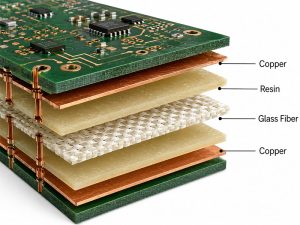
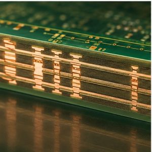
IS680 is a very low-loss PCB laminate used in RF and microwave circuits where signal loss, impedance drift and thermal stress can affect final performance. It is often reviewed for antennas, radar modules, RF front-end boards, communication equipment and high-frequency test hardware.
This guide explains what the material is, why it works, how the datasheet values compare, and whether it is easier to fabricate than PTFE. The focus stays on material selection, design review, testing, failure prevention and purchasing decisions for real PCB projects.
What Is IS680 PCB Material?
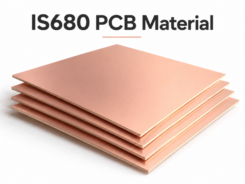
IS680 PCB material is a very low-loss laminate from Isola for RF and microwave PCB applications. It is designed for circuits that need lower dielectric loss than standard FR-4 and better manufacturing convenience than many PTFE-based laminates.
The material family covers several Dk grades, including 2.80, 3.00, 3.20, 3.33, 3.38 and 3.45. Names such as Isola IS680 280, Isola IS680-300 and IS680 338 usually refer to these dielectric constant grades.
In simple terms, this laminate sits between standard FR-4 and premium PTFE materials. It helps control RF performance while keeping the board closer to standard PCB fabrication.
Why Is IS680 Used in RF and Microwave PCB Applications?
IS680 is used in RF and microwave PCB applications because it controls dielectric loss, impedance stability and thermal reliability at the same time. These factors directly affect insertion loss, phase behavior, antenna tuning and signal consistency.
Main advantages include:
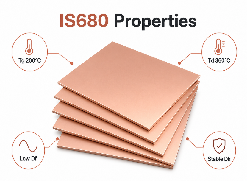
- Low Df for reduced dielectric loss in RF traces.
- Stable Dk for more predictable impedance calculation.
- High Tg for lead-free assembly and thermal cycling.
- Low moisture absorption for better environmental stability.
- Easier processing than many PTFE-based materials.
- Practical cost balance for commercial RF PCB projects.
Therefore, this material is often selected when the design needs reliable RF performance but does not justify a full PTFE stackup. For an IS680 ultra low loss PCB, the full signal path must also control copper roughness, dielectric spacing and connector transitions.
What Are the Dk and Df Values of Isola IS680?
The Isola IS680 dielectric constant depends on the selected grade. Common values include 2.80, 3.00, 3.20, 3.33, 3.38 and 3.45 at 10 GHz. The typical Df range is about 0.0025 to 0.0035.
| Grade | Dk | Df | Frequency |
|---|---|---|---|
| 280 | 2.80 | 0.0025 | 10 GHz |
| 300 | 3.00 | 0.0030 | 10 GHz |
| 320 | 3.20 | 0.0030 | 10 GHz |
| 333 | 3.33 | 0.0030 | 10 GHz |
| 338 | 3.38 | 0.0035 | 10 GHz |
| 345 | 3.45 | 0.0035 | 10 GHz |
The Dk value affects trace width, antenna size and phase delay. Lower Dk usually allows wider RF traces, while higher Dk can support more compact circuit layouts.
What Are the Main IS680 Laminate Properties?
IS680 laminate properties focus on electrical stability, thermal resistance and predictable fabrication. These properties help RF circuits keep stable behavior from prototype to batch production.
Important properties include:
- Dk range: 2.80 to 3.45 for different RF layout needs.
- Df range: about 0.0025 to 0.0035 for low-loss transmission.
- Tg: about 200°C for lead-free assembly margin.
- Td: about 360°C for stronger thermal decomposition resistance.
- Moisture absorption: about 0.10% for better humidity stability.
- Thermal conductivity: about 0.32 W/mK for standard laminate.
- Processing advantages: reduced drill wear, no plasma desmear and consistent dielectric spacing.
Isola IS680 Datasheet Overview
The Isola IS680 datasheet should be reviewed before stackup release because RF material data affects impedance, loss, thermal margin and fabrication control. The table below follows the official typical values.
| Property | Value | Unit | Method |
|---|---|---|---|
| Tg by DSC | 200 | °C | IPC-TM-650 2.4.25C |
| Td by TGA at 5% loss | 360 | °C | IPC-TM-650 2.4.24.6 |
| T260 / T288 | >60 | min | IPC-TM-650 2.4.24.1 |
| Z-axis CTE before Tg | 44.7 | ppm/°C | IPC-TM-650 2.4.24C |
| Z-axis CTE after Tg | 191 | ppm/°C | IPC-TM-650 2.4.24C |
| Z-axis expansion 50–260°C | 2.9 | % | IPC-TM-650 2.4.24C |
| X/Y-axis CTE before Tg | 12 | ppm/°C | IPC-TM-650 2.4.24C |
| Thermal conductivity | 0.32 | W/mK | ASTM E1952 |
| Thermal stress 10 sec at 288°C | Pass | Visual | IPC-TM-650 2.4.13.1 |
| Volume resistivity C-96/35/90 | 1.33 × 10⁷ | MΩ-cm | IPC-TM-650 2.5.17.1 |
| Surface resistivity C-96/35/90 | 1.33 × 10⁵ | MΩ | IPC-TM-650 2.5.17.1 |
| Dielectric breakdown | 45.4 | kV | IPC-TM-650 2.5.6B |
| Arc resistance | 139 | sec | IPC-TM-650 2.5.1B |
| Electric strength | 45 | kV/mm | IPC-TM-650 2.5.6.2A |
| CTI | 2 | Class | UL 746A / ASTM D3638 |
| Peel strength 1 oz EDC foil | 0.70 | N/mm | IPC-TM-650 2.4.8.2A |
| Flexural strength length | 37,500 | psi | IPC-TM-650 2.4.4B |
| Flexural strength cross | 28,500 | psi | IPC-TM-650 2.4.4B |
| Tensile strength length | 28,000 | psi | ASTM D3039 |
| Tensile strength cross | 26,000 | psi | ASTM D3039 |
| Poisson’s ratio length | 0.122 | — | ASTM D3039 |
| Poisson’s ratio cross | 0.120 | — | ASTM D3039 |
| Moisture absorption | 0.10 | % | IPC-TM-650 2.6.2.1A |
| Flammability | V-0 | Rating | UL 94 |
| Max operating temperature | 130 | °C | UL 796 |
Standard material offering includes 20, 30 and 60 mil laminate thicknesses, full sheet or panel form, HTE Grade 3 copper foil and copper weight from 1/2 oz to 2 oz. Heavier and thinner copper foil may be available by project review.
IS680 vs IS680 AG: What Is the Difference?
IS680 AG is the lower-loss related grade, while standard IS680 provides a wider Dk range. The difference matters when the design is sensitive to insertion loss, phase consistency and copper roughness.
| Item | IS680 | IS680 AG |
|---|---|---|
| Material class | Very low-loss laminate | Very low-loss laminate |
| Dk range | 2.80, 3.00, 3.20, 3.33, 3.38, 3.45 | 3.00, 3.38, 3.45, 3.48 |
| Df range | 0.0025 to 0.0035 | 0.0020 to 0.0029 |
| Tg | 200°C | 200°C |
| Td | 360°C | 360°C |
| Thermal conductivity | 0.32 W/mK | 0.38 to 0.53 W/m·K |
| Copper foil | HTE Grade 3 | HVLP or VLP2 |
| Copper weight | 1/2 to 2 oz | 1/2, 1 and 2 oz |
| Standard thickness | 20, 30, 60 mil | 20, 30, 60 mil |
| Glass style | Standard listed glass | Square weave and mechanically spread glass |
| Processing | Reduced drill wear, no plasma desmear | FR-4 process compatible, reduced drill wear, no plasma desmear |
| Best use | RF and microwave PCB with balanced cost | Lower-loss antenna and RF PCB with tighter loss control |
Choose the AG family when the design needs lower Df, smoother copper and better RF path consistency. Choose standard IS680 when the Dk grade range, material cost and production target are already suitable.
IS680 vs PTFE: How Are They Different?
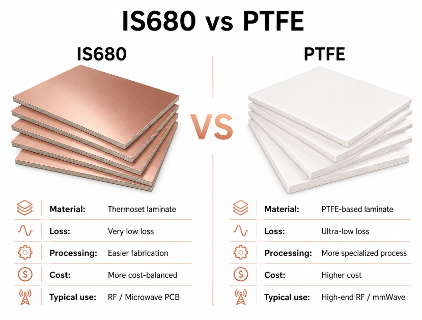
IS680 vs PTFE is mainly a comparison between process-friendly thermoset RF laminate and higher-end PTFE-based microwave laminate. PTFE can provide very low dielectric loss, but it often brings more difficult drilling, bonding, hole preparation and dimensional control.
| Item | IS680 | PTFE |
|---|---|---|
| Resin system | Thermoset low-loss laminate | PTFE-based laminate |
| Typical loss level | Very low | Very low to extremely low |
| Dk behavior | Stable from -55°C to +125°C up to W-band frequencies | Very stable, grade-dependent |
| Df behavior | 0.0025 to 0.0035 | Often lower, grade-dependent |
| Fabrication difficulty | Closer to standard PCB process | More specialized process |
| Drilling | Reduced drill wear listed | Softer material can need tighter control |
| Desmear / hole prep | No plasma desmear required | Plasma or special hole treatment may be required |
| Dimensional stability | Easier to control in many commercial builds | More sensitive in some builds |
| Copper adhesion | Standard PCB fabrication route | Bonding surface treatment may require more care |
| Cost level | More balanced | Usually higher |
| Typical board type | Commercial RF, microwave and antenna PCB | Demanding microwave, mmWave and defense PCB |
| Best purchasing fit | Cost-performance RF production | Highest RF performance when budget allows |
How to choose:
- Choose IS680 when the project needs low loss, stable Dk and easier RF PCB fabrication.
- Choose PTFE when the design has very strict loss, phase or mmWave requirements.
- Choose the thermoset laminate when lead time, cost, panel yield and production repeatability matter more.
- Choose PTFE only after confirming the supplier can manage drilling, bonding, plating and dimensional control.
For uncertain cases, build a prototype and compare insertion loss, impedance and antenna tuning before batch production.
How Does IS680 Compare with Other Low-Loss PCB Materials?
IS680 compares well with other low-loss PCB materials when the project needs balanced electrical performance, thermal reliability and easier processing. The right material depends on loss budget, copper foil, layer count, thickness and frequency range.
| Material | Dk Range | Df Range | Position |
|---|---|---|---|
| IS680 | 2.80 to 3.45 | 0.0025 to 0.0035 | Very low-loss RF laminate |
| IS680 AG | 3.00 to 3.48 | 0.0020 to 0.0029 | Lower-loss related grade |
| Astra MT77 | Around 3.00 | Around 0.0017 | Ultra-low-loss RF laminate |
| I-Tera MT40 | Around 3.38 to 3.75 | Around 0.0028 to 0.0035 | Low-loss digital and RF laminate |
| FR408HR | Around 3.68 | Around 0.0092 | High-speed digital laminate |
For strict insertion loss targets, a lower-Df material may be better. For commercial RF boards that require stable output and easier production, this laminate remains a strong candidate.
What Applications Commonly Use IS680 PCB Material?
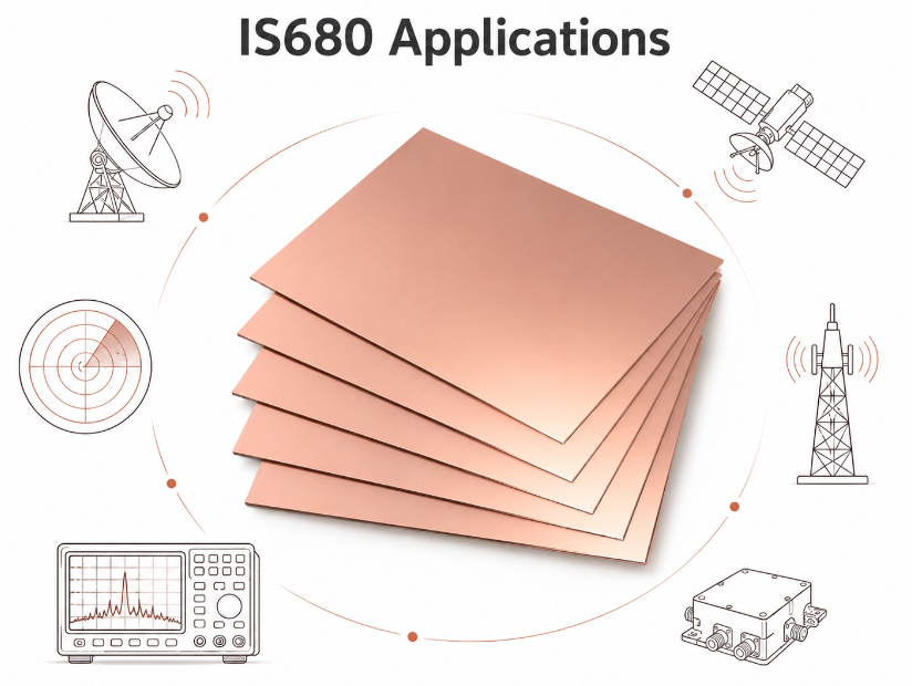
IS680 PCB material is commonly used in RF, microwave, antenna and communication PCB applications. It is selected when dielectric loss, phase shift and impedance variation can reduce product performance.
Common applications include:
- RF front-end modules.
- Microwave communication boards.
- Antenna feed networks.
- DAS and CPE antenna PCB designs.
- Radar module PCB.
- Satellite communication equipment.
- Aerospace and defense electronics.
- RF filters and couplers.
- Point-to-point microwave links.
- High-frequency test and measurement boards.
In these products, a poor laminate choice can shift frequency response, reduce gain or increase insertion loss. That is why the material should be reviewed before final stackup and layout release.
What Should You Check Before Choosing IS680 PCB Material?
Before choosing IS680 PCB material, review the real working frequency, loss target, Dk grade, stackup, copper foil, production process, testing method and purchasing plan. A suitable RF laminate must match the complete PCB design, not only one datasheet value.
- Frequency range: Confirm whether the product works in RF, microwave, W-band-related test conditions or a lower communication band. Higher frequency makes Dk tolerance, copper roughness and etching accuracy more important.
- Dk grade: Select 2.80, 3.00, 3.20, 3.33, 3.38 or 3.45 according to impedance, trace width, antenna size and layout space. Lower Dk usually gives wider RF traces, while higher Dk can reduce circuit size.
- Df target: Check the insertion loss budget before choosing the material grade. If the loss target is tight, compare standard laminate with AG grade or another lower-loss material.
- Copper foil: Review HTE, HVLP or other copper choices because conductor loss can become as important as dielectric loss. Smoother copper is useful for long RF paths and antenna feed networks.
- Dielectric thickness: Confirm whether standard 20, 30 or 60 mil cores can meet the impedance target. Non-standard thickness may affect cost, availability and production schedule.
- Layer count: Double-sided RF PCB is simpler, while multilayer or hybrid boards need lamination review, copper balance and via reliability control.
- Via transition: RF vias, ground stitching and connector launches should be checked before production. Poor via transitions can create reflection even when the laminate is correct.
- Surface finish: Choose the finish based on solderability, shelf life and RF contact areas. Edge-launch connectors and exposed pads need flatness and stable contact performance.
- Solder mask: Confirm whether solder mask should be kept away from RF traces or antenna sections. Solder mask can shift impedance and frequency response in sensitive areas.
- Manufacturing tolerance: Review line width, spacing, copper thickness, registration and etching tolerance. RF performance can move when geometry changes slightly.
- Test plan: Define impedance test, insertion loss test, TDR, AOI, microsection, copper thickness check, final electrical test and visual inspection before order release.
- Reliability target: Confirm IPC class, UL, RoHS, reflow profile, thermal stress and operating temperature. High-reliability products should not rely on material name alone.
- Cost factors: Board size, thickness, copper weight, layer count, surface finish, RF test scope, laminate availability and delivery schedule all affect price.
- Supplier capability: Work with a source factory that can review RF stackup, support custom PCB fabrication, control impedance and provide global delivery without false local-office claims.
FAQs About IS680 PCB Material
Q1: Can this material be stored like standard RF laminate?
A1: Store it in a clean, dry and temperature-controlled environment. Keep sheets sealed before production and avoid long exposure to humidity. Moisture absorption is about 0.10%, but poor storage can still affect lamination, soldering and electrical consistency.
Q2: Does this laminate support lead-free reflow?
A2: Yes, the material has Tg 200°C and Td 360°C, which gives thermal margin for lead-free assembly. However, thick boards, large copper areas and heavy components still need reflow review to prevent warpage, blistering or pad stress.
Q3: Can it be used in hybrid PCB stackups?
A3: Yes, but hybrid stackups need careful CTE, resin flow and lamination review. When RF laminate is combined with FR-4 or another material, dielectric spacing and via reliability must be checked. Hybrid designs should be approved before mass production.
Q4: What surface finish is better for RF areas?
A4: The right finish depends on soldering, storage and RF contact design. ENIG, immersion silver, immersion tin and OSP can be reviewed. For connector launch areas, flatness, contact resistance and insertion loss are more important than a general finish preference.
Q5: Does solder mask affect RF traces?
A5: Yes. Solder mask adds dielectric material above the trace and can change impedance or antenna tuning. For sensitive RF lines, designers often expose or keep mask away from selected areas. Confirm solder mask rules before impedance calculation.
Q6: Can it replace Rogers material in every design?
A6: No. It can replace some RF laminates only when Dk, Df, thickness, copper foil and loss targets match the design. Do not replace a proven material only by matching Dk. Prototype testing is needed for antennas, filters and long RF paths.
Q7: What causes batch variation in RF PCB performance?
A7: Batch variation usually comes from dielectric thickness tolerance, copper roughness, etching shift, plating thickness, connector launch differences or uncontrolled solder mask. Stable material helps, but process control decides repeatability.
Q8: Is special testing needed for antenna PCB?
A8: Yes. Standard electrical testing only checks opens and shorts. Antenna PCB may need impedance, insertion loss, return loss, resonance frequency or gain-related testing. RF testing should be defined before quotation, not after production.
Q9: What files should be sent for a quote?
A9: Send Gerber files, drill files, stackup, Dk grade, board thickness, copper weight, surface finish, impedance tolerance, test requirement, quantity and delivery target. For RF products, also send frequency range and insertion loss limits when available.
Q10: Why does price vary between similar RF boards?
A10: Price changes with laminate grade, panel use, layer count, copper foil, thickness, tolerance, surface finish, drilling difficulty, RF testing and material lead time. Two boards using the same laminate can still have very different production costs.
Q11: What should be checked before batch production?
A11: Build a prototype first, then check impedance, insertion loss, connector launch, soldering quality and dimensional stability. Confirm the material grade and stackup on the fabrication drawing. Do not move to batch production before RF results are verified.
Conclusion
IS680 is a strong RF and microwave PCB material when a project needs stable Dk, low Df, high thermal resistance and easier fabrication than many PTFE-based materials. It fits antenna, radar, communication, aerospace, RF module and test equipment projects where signal loss and production repeatability matter.
For selection, compare the Dk grade, Df value, copper foil, dielectric thickness, stackup, surface finish, RF test scope and real production tolerance before release. A correct material choice can reduce redesign risk, improve batch consistency and control total procurement cost.
EBest Circuit is a China source factory for custom PCB and PCBA manufacturing with global supply support. Send your IS680 PCB files, stackup, quantity and test requirements to sales@bestpcbs.com for a fast quotation.