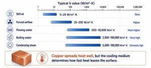
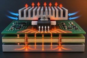
Copper thermal conductivity vs temperature data can look precise while still producing the wrong PCB decision. The commonly quoted room-temperature value describes bulk copper under defined conditions; it does not automatically represent a finished board, a plated feature, or the complete component-to-cooler heat path.
PCB buyers therefore need to confirm the copper temperature and condition, the released stackup and heat-spreading geometry, and the drawings, fabrication limits, and test inputs required before production. This guide turns reference conductivity data into concise, manufacturable PCB checks.
Copper Thermal Conductivity vs Temperature Chart
Copper is often assigned a single thermal conductivity value, but that shortcut can mislead a PCB thermal review. The value depends on temperature, material condition, and purity. It also describes bulk copper—not the effective thermal conductivity of a finished multilayer board.
The table below is a practical reference for pure copper from 100 K to 1,200 K. It shows the expected downward trend as temperature rises through the range relevant to many industrial calculations.
| Temperature (K) | Approx. temperature (°C) | Thermal conductivity k (W/m·K) |
|---|---|---|
| 100 | -173 | 480 |
| 150 | -123 | 429 |
| 200 | -73 | 413 |
| 250 | -23 | 406 |
| 300 | 27 | 401 |
| 400 | 127 | 393 |
| 600 | 327 | 379 |
| 800 | 527 | 366 |
| 1,000 | 727 | 352 |
| 1,200 | 927 | 339 |
For an ordinary PCB operating near room temperature, 401 W/m·K is a reasonable first-pass value for bulk copper. For a high-temperature calculation, use a value matched to the expected copper temperature—not the ambient air temperature—and retain margin for interfaces and manufacturing variation.
Copper Thermal Conductivity Temperature Dependence Explained
In copper, mobile electrons carry most of the heat. As temperature rises, atomic vibrations increase and scatter those electrons more frequently. The result is lower thermal conductivity across the normal and elevated-temperature range.
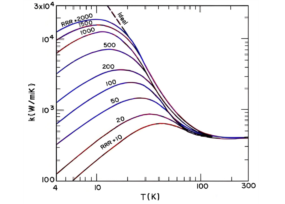
The behavior is not one simple straight line across every temperature. At cryogenic temperatures, conductivity can rise sharply to a peak and then fall again near absolute zero. The peak is highly sensitive to purity and defects, so a room-temperature copper value cannot be extended into a cryogenic model.
- Temperature range: State the minimum, normal, and maximum copper temperature used in the calculation.
- Copper condition: Identify the relevant copper grade, temper, plating, and any alloyed or bonded layers.
- Heat-flow direction: Separate in-plane spreading through copper from through-board heat flow across dielectric layers.
- Boundary conditions: Define the heat source, contact area, cooling interface, airflow, and allowed temperature rise.
A useful supplier question is not only “What is copper’s k value?” It is “Which value and temperature range were used in the thermal model, and does the released stackup support that heat path?”
Thermal Conductivity of Copper at Various Temperatures
Published datasets agree on the broad room-to-high-temperature trend: copper is near 400 W/m·K around room temperature and gradually declines as temperature rises. One Zenodo dataset lists 401 W/m·K at 273 K, 398 W/m·K at 300 K, 392 W/m·K at 400 K, and 383 W/m·K at 600 K.
Cryogenic data require more care. NIST publishes OFHC copper curve fits from 4 K to 300 K for several residual resistance ratio (RRR) values. RRR is a practical indicator of purity and defect scattering; higher-RRR copper can reach a much larger low-temperature conductivity peak than ordinary copper.
- Room and elevated temperatures: Use a temperature-matched value and document the source.
- Cryogenic service: Specify the copper grade and an appropriate RRR assumption or material certificate.
- Wide operating range: Use a curve or temperature bands instead of one constant value.
- Production release: Keep the thermal-model assumption aligned with the copper actually purchased and fabricated.
For PCB purchasing, do not request “high-purity copper” as an undefined phrase. Put the required copper specification, thickness, finished-copper tolerance, surface finish, and any evidence requirement into the drawing or procurement package.
What Is the Thermal Conductivity of Copper at Room Temperature?
At approximately 20-27°C, pure copper is commonly treated as about 400-401 W/m·K. That number is useful for material comparison and early thermal estimates, but it should not be copied directly into a board-level claim.
A PCB contains copper foils, plated holes, resin, glass reinforcement, solder mask, surface finish, solder, components, and interfaces. The copper may spread heat efficiently along the plane of a layer, while through-thickness heat transfer is restricted by dielectric materials and small contact areas.
- Use 401 W/m·K: For a documented first-pass bulk-copper estimate near room temperature.
- Use a lower temperature-specific value: When copper operates well above room temperature.
- Use effective PCB properties: When modeling the complete stackup or through-board heat flow.
- Use test correlation: When temperature limits are tight, interfaces dominate, or safety/reliability depends on the prediction.
Before RFQ, the customer should identify whether the value applies to raw copper, a copper feature, one PCB layer, or the assembled thermal path. This prevents a material constant from becoming an unsupported finished-product requirement.
Copper Conductivity vs Temperature for PCB Heat Spreading
Temperature-dependent copper conductivity matters, but geometry usually controls whether the available copper can move enough heat. A thin trace and a wide copper plane can use the same material value while producing very different temperature rises.
- Copper thickness and area: Confirm base copper, finished copper, plating contribution, plane coverage, neck-downs, and current/heat bottlenecks.
- Layer location: Identify whether the principal heat-spreading layer is external or buried and what dielectric separates it from the source.
- Thermal vias: Define finished hole size, plating, quantity, pitch, fill/cap requirements, and the receiving copper area.
- Interfaces: Include solder joints, thermal pads, dielectric layers, coatings, mounting pressure, and contact resistance in the model.
- Manufacturing tolerances: Review whether minimum feature sizes, annular rings, registration, copper balance, and finished thickness can support the proposed heat path.
EBest Circuit (Best Technology) can review the released PCB data for manufacturability, stackup, copper distribution, via structures, fabrication, assembly, inspection, and test coordination. The customer remains responsible for system heat loads, component junction limits, airflow, enclosure cooling, and final product validation unless a separate scope is agreed.
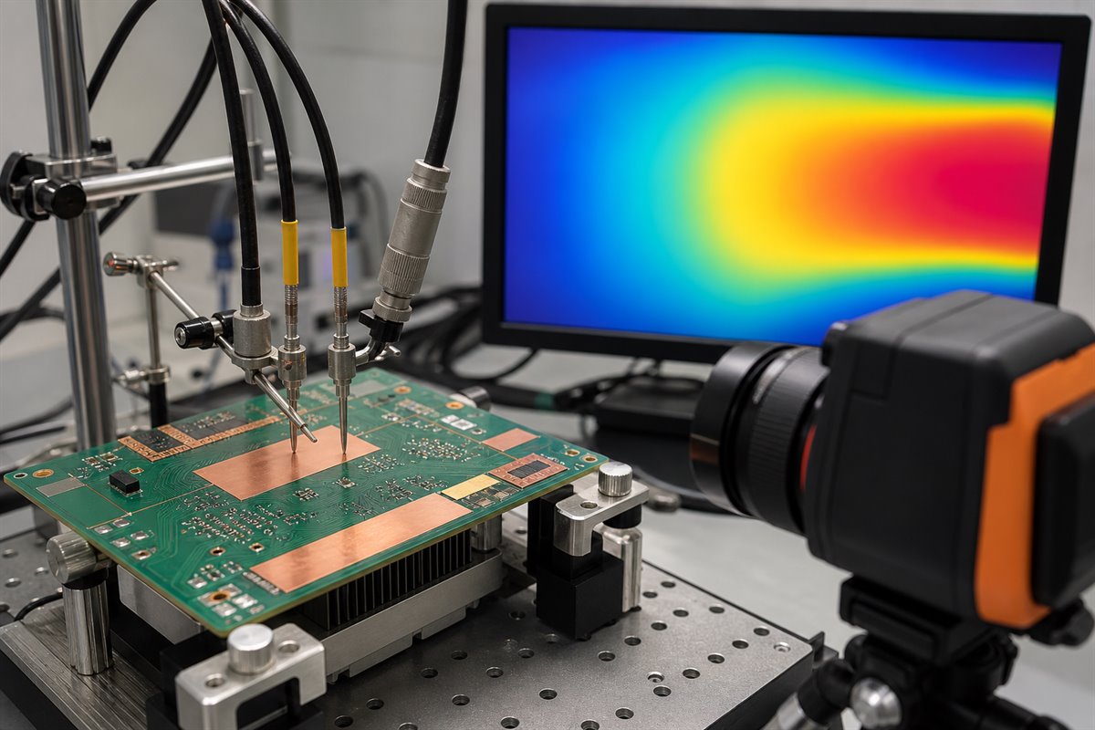
Copper Thermal Conductivity vs Aluminum for PCB Tradeoffs
At room temperature, copper conducts heat substantially better than aluminum: approximately 401 W/m·K versus about 237 W/m·K for pure aluminum. Copper can therefore move more heat through the same idealized cross-section, but conductivity alone does not select the best PCB construction.
| Decision factor | Copper | Aluminum-base option |
|---|---|---|
| Thermal conductivity | About 401 W/m·K | About 237 W/m·K |
| Weight | Heavier | Lighter |
| PCB role | Foil, planes, and vias | Metal-core base |
| Buyer check | Copper geometry | Dielectric and base |
Choose the construction by the complete heat path, electrical isolation, weight, mechanical needs, achievable geometry, cost, and validation plan. A copper-heavy FR-4 board, an MCPCB, and a ceramic PCB solve different constraints; none should be selected from one W/m·K number alone.
PCB Project Example: Copper Thermal Conductivity in Heat-Spreading Checks
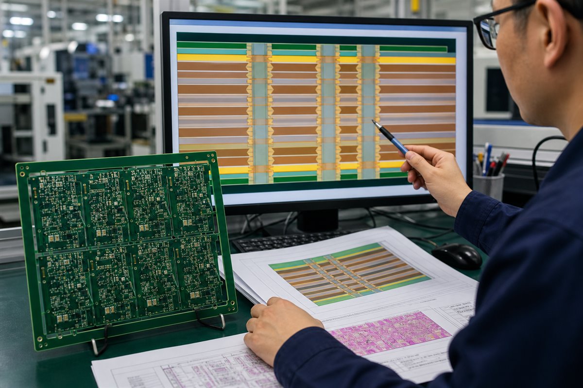
In one customer order, EBest Circuit reviewed a compact 47 × 34.5 mm, 12-layer FR-4 TG180 PCB built to IPC Class 3. The build combined blind vias from L1-L2 and L12-L11, buried vias from L2-L11, resin-plugged and plated-flat vias, a 2.0 mm finished thickness, and ENIG. Before production, the customer required the production stackup and CAM artwork for approval.
The thermal and manufacturing concern was not selecting another handbook conductivity value. The order data did not confirm the proposed 1 oz outer copper, while the residual copper area differed significantly among layers. Those details affect the real heat-spreading geometry, copper balance, and buildability even though bulk copper near room temperature remains about 401 W/m·K.
- Outer-copper clarification: The customer had not confirmed 1 oz outer copper. EBest Circuit therefore kept it open in the EQ and production stackup instead of treating it as an approved input.
- Via feasibility: The blind/buried sequence and resin-plugged, plated-flat vias required manufacturing review. The customer retained a ±2 mil via tolerance, so the released drawing and inspection basis had to preserve that decision.
- Test-coupon confirmation: The COC mentioned a test coupon, but this order did not include impedance control. The customer confirmed that no coupon was needed, so the production documents were aligned with the agreed scope.
- Copper balance decision: Because residual copper differed substantially by layer, engineering recommended a 1.0% bow-and-twist control. The customer did not accept the recommendation, so the decision was recorded and the production data remained customer-controlled.
- Release gate: EBest Circuit issued the production stackup and CAM artwork for customer approval. Production could begin only after those documents were confirmed.
This order shows why copper thermal conductivity must be checked together with the actual stackup and released copper geometry. The credible supplier action was to surface unresolved data, preserve the customer's decisions, and gate production on approved manufacturing documents—not to claim that the 401 W/m·K material value alone guaranteed board temperature.
Copper Thermal Conductivity vs Temperature FAQs
Does copper thermal conductivity decrease as temperature increases?
Across typical room and elevated-temperature ranges, yes. Reference tables show a gradual decline as temperature rises. Cryogenic behavior is different and depends strongly on purity and RRR.
What copper thermal conductivity value should I use at room temperature?
About 400-401 W/m·K is a common bulk-copper reference near 20-27°C. State the source and do not treat it as the effective conductivity of the complete PCB.
Can I use one copper conductivity value for the full PCB temperature range?
Only for a rough model over a narrow range with adequate margin. For wide or critical ranges, use temperature-dependent data or defined temperature bands and correlate the model with testing.
Does thicker copper automatically solve a PCB hotspot?
No. Thickness can help, but plane area, bottlenecks, layer position, vias, dielectric interfaces, component attachment, and cooling boundary conditions also control the result.
What should I send for a PCB thermal and DFM review?
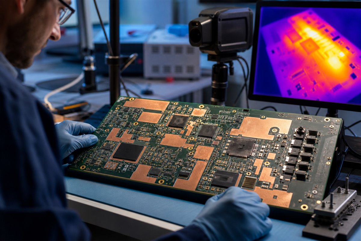
Send the controlled fabrication data, stackup, finished-copper requirements, drill data, BOM and placement data for assembly, expected operating range, heat-source information, thermal-interface assumptions, and the temperatures or test points that must be verified.
For a copper thermal conductivity vs temperature manufacturability review, contact EBest Circuit (Best Technology) at sales@bestpcbs.com with the controlled board package and operating assumptions. The review can then focus on the files, tolerances, heat-spreading features, and verification inputs that affect fabrication and assembly risk.