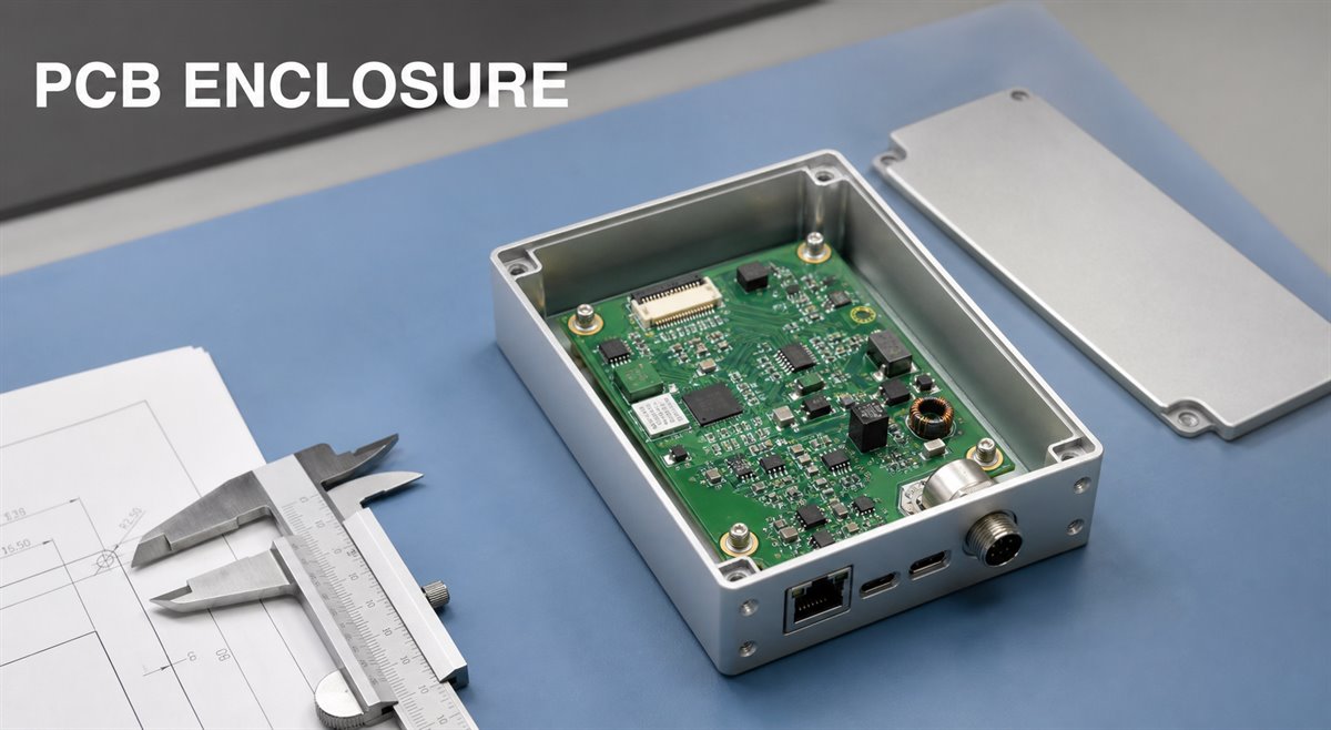
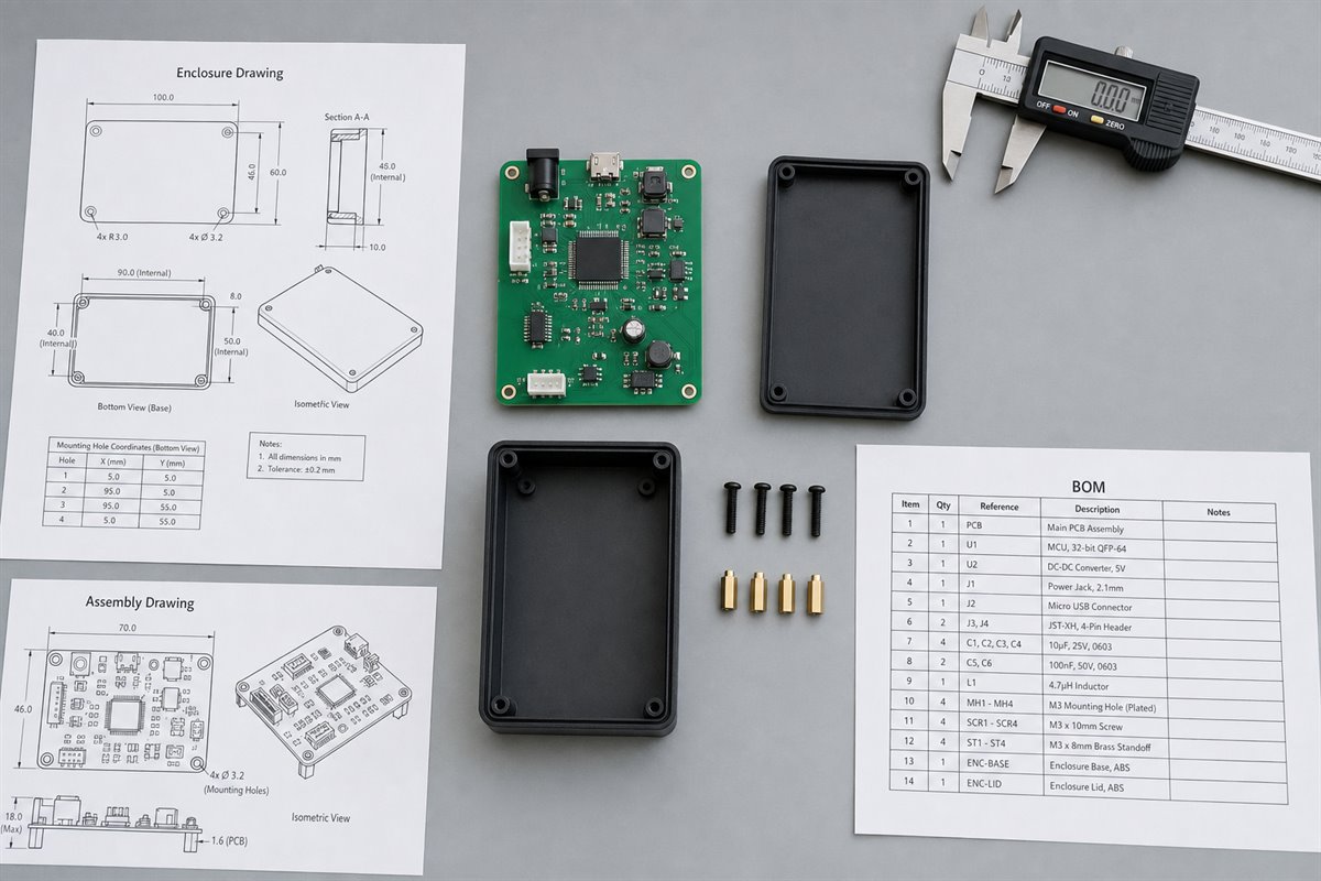
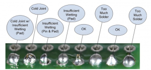
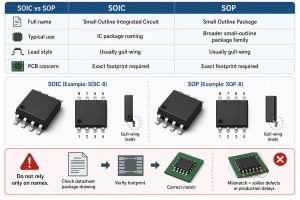
An enclosure case aluminum pcb project combines a printed circuit board or PCBA with an aluminum housing that provides mechanical protection, connector access, heat spreading and electromagnetic shielding. Reliable integration depends on more than selecting a box that appears large enough. The PCB outline, mounting system, component height, panel cutouts, grounding points, thermal interfaces and manufacturing tolerances must be developed as one assembly.
What Does Enclosure Case Aluminum PCB Mean?
The phrase normally describes a PCB installed in an aluminum electronics enclosure. The enclosure may be an extruded profile with internal card guides, a two-piece die-cast box, a folded sheet-metal housing or a machined aluminum body. The circuit board can be standard FR4, high-Tg FR4, an RF laminate, a metal-core board or another construction selected for the electrical and thermal load.
The enclosure and PCB have separate manufacturing data. PCB files define copper, drill, solder mask, board outline and assembly details. Enclosure drawings define cavity dimensions, wall thickness, rails, bosses, threaded holes, panel cutouts, surface finish and sealing features. A single mechanical datum scheme must relate the two data sets so that a connector, switch or indicator lands in the intended panel opening after all tolerances are applied.
How Is an Aluminum Enclosure Different from an Aluminum PCB?
An aluminum enclosure is a mechanical housing. An aluminum PCB is a circuit substrate, usually an insulated metal substrate with a copper circuit layer, dielectric layer and aluminum base. Either one can exist without the other: a conventional FR4 control board can sit inside an aluminum case, while an aluminum PCB can be mounted in a polymer housing.
| Item | Primary function | Design-controlled features |
|---|---|---|
| Aluminum enclosure | Protection, structure, shielding and possible heat spreading | Internal cavity, rails, bosses, panel openings, seals and finish |
| Aluminum PCB or MCPCB | Electrical interconnection with a thermally conductive metal base | Circuit pattern, dielectric, metal base, board thickness and surface finish |
| FR4 PCB in an aluminum case | General signal, control and power circuitry inside a conductive housing | Stack-up, mounting, clearance, grounding and connector alignment |
When heat must pass from components through the circuit board to the housing, a metal-core PCB can reduce part of the thermal path. It does not eliminate the need to calculate interface resistance, contact pressure and the enclosure-to-ambient path.
Which Aluminum Enclosure Type Fits a PCB Assembly?
The enclosure type should follow the required production volume, environmental protection, machining burden, thermal path and service method. An extruded aluminum case is practical for rectangular electronics because the profile can include PCB rails and only the end plates require most connector openings. Die-cast cases provide robust walls and sealing options, but their draft angles and internal radii reduce usable cavity space. Sheet-metal housings are efficient for larger or lower-profile equipment and permit formed brackets, although bend tolerances must be included in the stack-up.
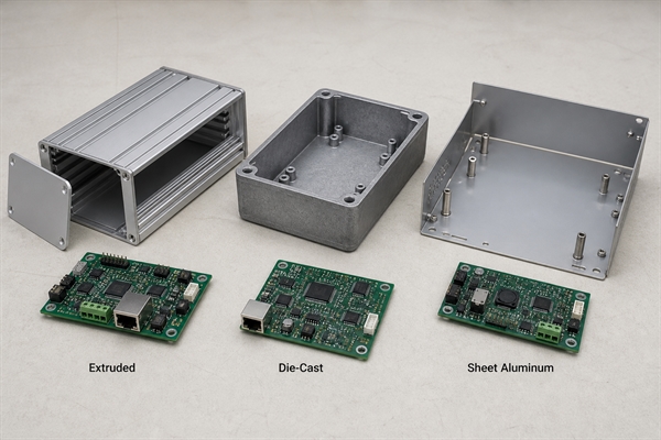
| Enclosure type | Best fit | PCB integration concern |
|---|---|---|
| Extruded profile | Controllers, instruments and power modules with a consistent cross-section | Rail width, board insertion path and end-panel connector alignment |
| Die-cast box | Rugged or sealed assemblies with moderate production volume | Boss locations, corner radii, draft and conductive finish at grounding points |
| Sheet aluminum | Larger chassis, rack equipment and low-profile electronics | Bend tolerance, PEM hardware, panel flex and cable routing |
| Machined enclosure | Low-volume precision, RF or specialized thermal assemblies | Cost, datum control and avoidance of unnecessary machining detail |
A sealed housing also needs a pressure and moisture strategy. Gaskets, cable glands and vents affect available panel space, while trapped heat can make an enclosure with a high IP rating run hotter than an open laboratory prototype.
How Should the PCB Outline and Internal Rails Be Matched?
For a rail-mounted board, specify the finished PCB thickness together with the rail slot width and positional tolerance. Nominal 1.6 mm FR4 is not an exact dimension; copper, laminate, solder mask and fabrication tolerance influence the finished thickness. The rail must provide insertion clearance without allowing enough lateral movement to misalign connectors or create vibration wear.
The enclosure drawing should state the usable rail depth, entry chamfer, internal corner radius and obstruction-free insertion path. The PCB drawing should state the finished outline tolerance, board thickness tolerance and any edge bevel. Keep copper, plated features and fragile components away from sliding edges. If the board enters at an angle before seating, model the swept volume rather than checking only the final position.
Card-edge grounding requires a separate decision. A bare copper or plated edge contact can provide controlled chassis connection, while solder mask on the rail edge prevents an unintended electrical path. Anodized aluminum is electrically insulating at the surface, so apparent metal-to-metal contact should never be assumed to be a reliable ground.
How Should Mounting Holes, Standoffs and Keepouts Be Designed?
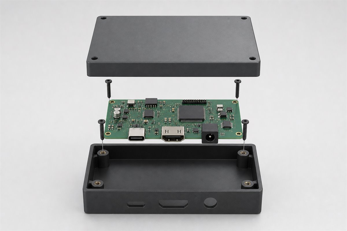
Standoff locations should restrain the PCB without bending it during screw installation, connector mating or cable handling. Place support near high insertion-force connectors and heavy components, but maintain access for drivers and inspection. Three well-positioned supports define a plane; additional standoffs require tighter coplanarity control to avoid forcing a warped board against the enclosure.
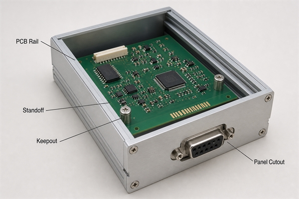
- Size non-plated mounting holes for screw clearance plus PCB and enclosure positional tolerance.
- Use plated mounting holes only when the electrical connection is intentional and the current path is defined.
- Keep copper, vias and components outside washer, screw-head and standoff contact zones.
- Check underside lead protrusion against the standoff height and enclosure floor.
- Define whether insulating washers, shoulder bushings or nylon hardware are required.
- Reserve tool access so the assembly sequence does not depend on an angled or partially engaged screw.
A mounting-hole keepout is not only a circle around the drill. It must cover screw-head sweep, washer diameter, driver access, possible standoff misalignment and any conductive debris created during service.
How Do Connectors and Panel Cutouts Affect PCB Layout?
Panel-mounted connectors establish some of the most important PCB datums. Define the connector mating face, centerline and height from the same enclosure reference used for the cutout. The footprint courtyard alone may not include shell tabs, latch motion, cable overmold or the hand clearance needed to mate the connector.
Allow for PCB positional tolerance, connector placement tolerance, reflow movement and panel machining tolerance. A cutout should clear the connector body without becoming so large that it weakens the panel, exposes internal circuitry or defeats an EMI gasket. For USB, RJ45, D-sub, circular and terminal-block interfaces, check the actual production part rather than relying on a generic model.
Front-panel LEDs and light pipes require optical alignment as well as mechanical clearance. Switches need travel clearance and force transfer without flexing the PCB. If a connector is mechanically fixed to the panel and soldered to the board, avoid a fully constrained geometry that transfers panel tolerance directly into solder joints.
How Does an Aluminum Case Change PCB Thermal Design?
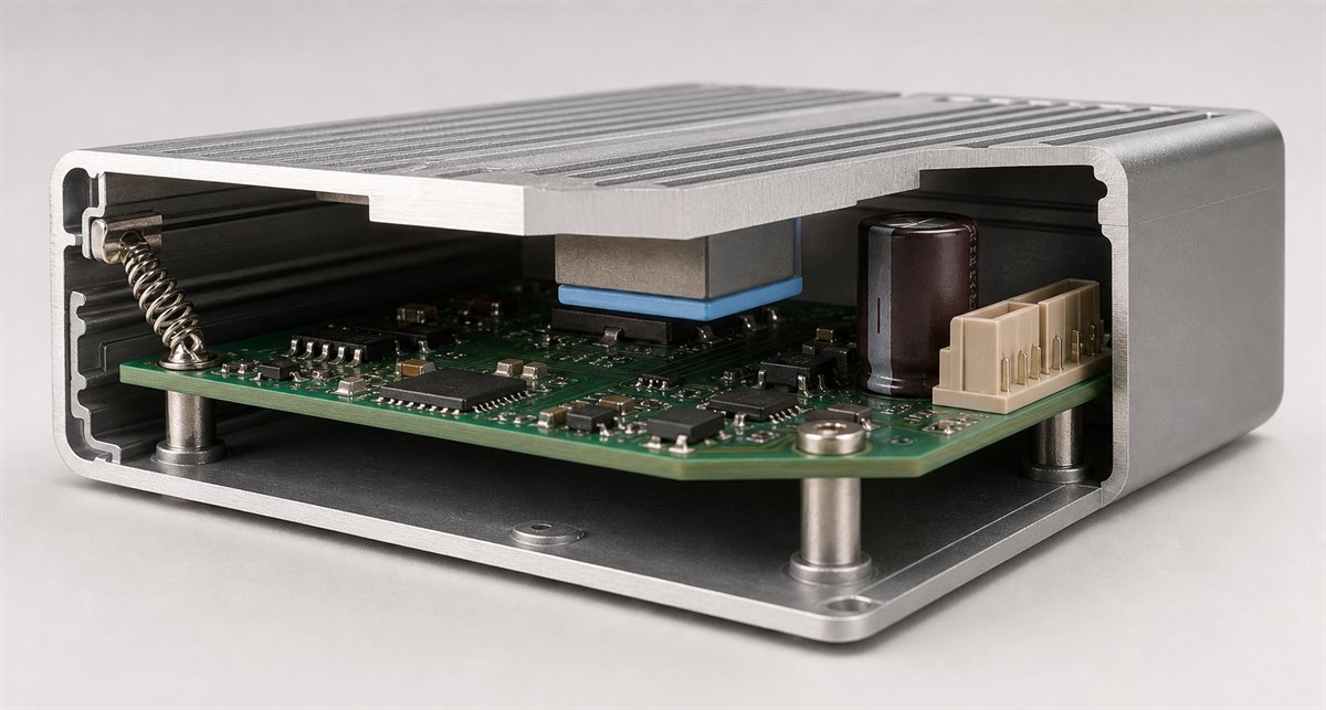
Aluminum spreads heat well, but the housing becomes useful only when a controlled path connects the heat source to it. The complete path may include the component junction, package, solder joint, PCB copper, thermal vias or metal core, thermal interface material, enclosure wall and external convection. The largest temperature drop can occur across a thin-looking interface if contact area or pressure is poor.
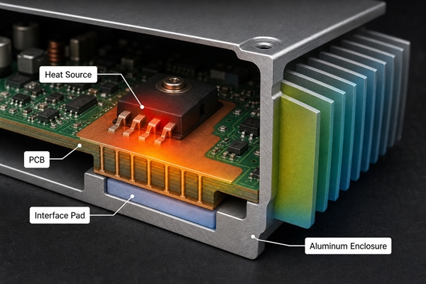
Begin with the allowable component junction temperature and ambient range, then allocate thermal resistance across the path. Use interface pads only where compression is controlled; an excessively thick pad accommodates tolerance but increases thermal resistance. Avoid routing high-current or temperature-sensitive circuits through a clamping zone without evaluating mechanical stress.
For a standard FR4 PCB, copper planes and thermal vias can move heat toward a chassis contact area. Higher heat flux may justify MCPCB, a local copper coin, a bonded heat spreader or direct component-to-housing contact. The correct choice follows heat density and electrical isolation requirements, not the presence of an aluminum case alone.
How Should Grounding and EMI Shielding Be Planned?
A conductive enclosure can reduce radiated emissions and improve immunity, but seams, apertures, cable shields and poorly controlled contacts can dominate performance. Decide where circuit ground connects to chassis, whether the connection is direct or capacitive, and whether one point or multiple low-inductance points are required by the frequency range.
Remove or mask anodizing at designated bonding locations, then use compatible hardware and controlled contact pressure. Star washers can penetrate surface films but may damage finishes and create debris; conductive gaskets or plated bonding pads provide more repeatable high-frequency contact when designed correctly. Keep the chassis connection short and wide because a long trace or wire adds inductance.
Connector shields should usually meet the enclosure at the entry point rather than carrying high-frequency current across the PCB before reaching chassis. Panel gaps, ventilation slots and display windows must be evaluated against the relevant wavelength and immunity environment. Verify the completed assembly, because a bare-board EMC test cannot represent enclosure seams and cable exits.
How Can Galvanic Corrosion and Electrical Shorts Be Prevented?
Aluminum, copper, nickel-plated parts and steel fasteners can form galvanic couples when moisture and an electrical path are present. Material pairing, surface finish, sealing and drainage should be chosen for the expected environment. Do not remove anodizing over a broad area merely to obtain ground; create small, controlled bonding points and protect the surrounding surface.
Electrical insulation needs positive dimensions. Maintain clearance between exposed conductors and the enclosure under the worst PCB position, board bow and hardware tolerance. Add insulating films, shoulder washers or barriers where a single shifted board could contact metal. Confirm that solder tails, clipped leads and through-hole pins cannot reach the enclosure floor after assembly.
Service operations also matter. Loose screws, metal chips from field drilling and damaged insulating pads can create faults after the product passed factory test. Captive hardware, deburring, cleaning and clear replacement-part control reduce these risks.
Which Tolerances Must Be Controlled Between PCB and Enclosure?
PCB-to-enclosure fit is a tolerance-chain problem. Choose a primary datum, usually a mounting feature or panel reference, and calculate the extreme position of each critical feature from that datum. Do not independently dimension every feature from different enclosure edges; accumulated ambiguity makes inspection and troubleshooting difficult.
| Critical relationship | Contributors to the tolerance chain | Practical control |
|---|---|---|
| Connector to panel opening | PCB outline, hole position, standoff, connector placement and cutout position | Common datum plus verified production connector model |
| PCB edge to rail | Finished board width, thickness, rail width, extrusion straightness and finish | Rail-fit coupon or first-article insertion test |
| Component to lid | Component height, solder stand-off, board bow, standoff height and lid flatness | Worst-case height stack with defined compression allowance |
| Thermal pad compression | Package height, PCB position, pad thickness and enclosure flatness | Compression range and contact-area inspection |
Use nominal dimensions for CAD assembly and worst-case dimensions for clearance validation. A prototype that happens to fit at nominal conditions does not prove production compatibility. First-article measurements should be compared with the controlled tolerance model, not just judged by whether the lid closes.
How Should an Enclosure PCB Assembly Be Prototyped and Tested?
Prototype validation should start before the final aluminum tooling is frozen. A rapid-machined panel, representative extrusion section or 3D-printed fit model can expose connector, cable and assembly-sequence problems. Thermal and EMC tests, however, require materials and conductive interfaces representative of production.
- Mechanical fit: verify insertion, fastener access, connector mating, cable bend radius, lid clearance and service removal.
- Electrical safety: measure clearance to the chassis and confirm intentional grounding points.
- Thermal operation: test at worst-case power, ambient and orientation after temperatures stabilize.
- EMI behavior: test with production-equivalent seams, cables, panel hardware and bonding surfaces.
- Vibration and handling: inspect board movement, connector loading, heavy-component support and fastener retention.
- Functional verification: repeat operation after enclosure assembly because clamping, grounding and heat can change behavior.
Photographs, measured gaps, torque values, temperatures and test conditions should be recorded against the same hardware revision. This turns prototype findings into manufacturing controls instead of informal observations.
Which PCB Technologies Suit Aluminum Enclosures?
Most control, communication and interface assemblies use rigid FR4 because it offers broad material, layer-count and impedance options. Metal-core boards suit concentrated LED or power heat sources when the circuit can use a metal-backed thermal path. Rigid-flex can reduce cable connectors in compact housings, while heavy-copper constructions support high current when conductor temperature rise is the dominant constraint.
EBest Circuit (Best Technology) supports PCB fabrication and PCB assembly for enclosure-integrated electronics rather than manufacturing the aluminum housing itself. Relevant programs can use SMT, through-hole or mixed assembly with 3D SPI, AOI, X-ray and functional testing selected for the package and failure risks. Website capability data lists standard PCB dimensions up to 610 x 610 mm and MCPCB dimensions up to 100 x 1,300 mm; extreme sizes remain subject to stack-up, material, panel utilization and engineering review.
For an enclosure project, the useful manufacturing package aligns the PCB outline and drill data with the controlled mechanical model, connector part numbers, component-height limits and grounding features. That alignment permits fabrication and assembly checks to catch mechanical risks before the completed PCBA reaches final housing integration.
FAQ About Enclosure Case Aluminum PCB
Can a PCB Touch an Aluminum Enclosure?
Only at intentionally designed mounting or grounding points. Exposed conductors, solder joints and lead ends need worst-case clearance from the housing. Use standoffs, insulating films or bushings where movement or tolerance could create unintended contact.
Does an Aluminum Enclosure Automatically Ground the PCB?
No. Anodized surfaces are electrically insulating, and painted or oxidized contact areas can be unstable. Define the chassis connection, surface preparation, hardware, torque and verification method.
Can an Aluminum Case Be Used as a Heat Sink?
Yes, when a calculated thermal path and controlled interface connect the heat source to the case. The enclosure surface area and airflow must then reject that heat to ambient without exceeding component or touch-temperature limits.
How Much Clearance Should a PCB Have Inside an Aluminum Case?
There is no universal value. Clearance must cover PCB outline tolerance, enclosure tolerance, board bow, component and hardware protrusion, assembly movement, electrical spacing and service access. Critical gaps should be calculated as a tolerance chain.
Are Extruded Aluminum Rails Suitable for Every PCB?
No. Rail-mounted boards need compatible finished thickness, edge keepouts and an unobstructed insertion path. Heavy components, tall connectors or vibration loads may require additional standoffs or brackets.
Conclusion
A successful enclosure case aluminum pcb design treats the board, components, connectors, aluminum housing and assembly process as one tolerance-controlled system. Select the enclosure form from environmental and production needs, then coordinate rails, mounting, panel openings, grounding, thermal interfaces and inspection datums before either design is frozen.
For PCB fabrication, MCPCB and PCBA support aligned with an aluminum enclosure design, contact EBest Circuit (Best Technology) at sales@bestpcbs.com.