A PCB enclosure project should reach assembly without hand-drilled openings, forced connectors or boards that no longer fit. Check the board outline, mounting holes, connector cutouts, component height, grounding and thermal interfaces before releasing orders, so your team can reduce rework, protect the schedule and receive a quote based on the real assembly scope.
Use this guide to confirm what your team should define and which files your manufacturer needs for a useful fit review. You keep control of the mechanical, electrical, thermal and EMC requirements; EBest Circuit (Best Technology) can review PCB manufacturability, fabricate the boards, support BOM sourcing and PCBA, and assist with agreed fit checks and testing against your released enclosure files.
What Is a PCB Enclosure, and Why Does Fit Matter?
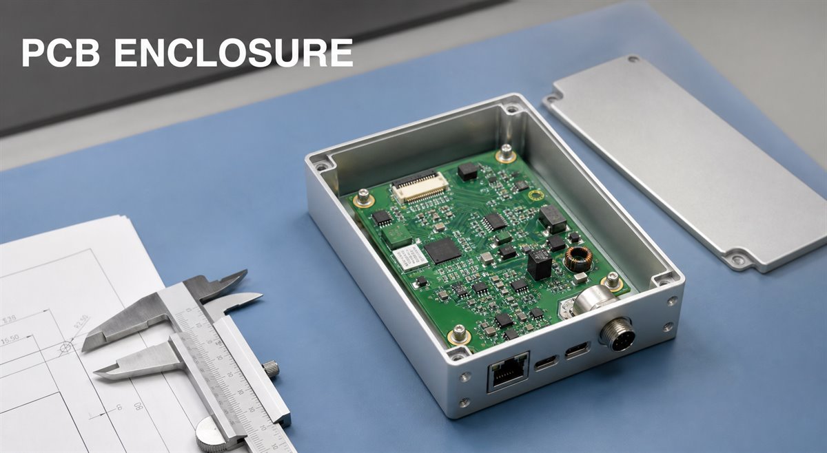
A correctly matched PCB enclosure helps your team move from prototype to repeat assembly without trimming boards, modifying housings or forcing parts into position. It is the housing around a bare PCB or assembled PCBA and may provide mechanical protection, environmental separation, user safety, cable organization, heat transfer, grounding or electromagnetic shielding.
To make that protection usable in production, check these interfaces together:
- The PCB outline must fit inside the internal cavity.
- Mounting holes must align with standoffs or brackets.
- Connectors, switches, indicators and displays must align with openings.
- Components must remain clear of the cover, walls, fasteners and cables.
- Grounding and shielding contacts must connect only where intended.
- Heat-producing components must work with the approved thermal path.
If the first assembled unit becomes the fit check, your team may face PCB rework, hand-machined housings, stressed connectors and an inaccurate assembly quotation. Check the mechanical model, PCB data and assembly information before ordering, and make sure every file describes the same released version.
Which PCB Enclosure Material Fits the Operating Environment?
Choosing the enclosure material early helps you avoid late changes to grounding, cooling, mounting hardware and cost. Material affects rigidity, weight, shielding behavior, heat transfer, insulation, machining options and corrosion exposure. The right choice depends on the environment and compliance requirements your team defines—not on a generic claim that one material is always better.
| Enclosure option | Common reason to consider it | Interface issue to confirm |
|---|---|---|
| Molded plastic | Electrical insulation, low weight, shaped features | Boss strength, wall movement and insert locations |
| Aluminum | Lower weight with conductive shielding and heat spreading potential | Grounding points, finish and galvanic contact |
| Steel | Rigidity and conductive shielding | Weight, corrosion protection and sharp-edge clearance |
| Die-cast or machined metal | Rigid structure and repeatable mechanical features | Tolerance, coating and thermal-interface flatness |
Before the enclosure material is released, confirm:
- indoor or outdoor use and expected temperature range;
- exposure to moisture, chemicals, dust, vibration or impact;
- insulation, grounding and shielding requirements;
- flammability or industry-specific requirements identified by the customer;
- surface finish or coating at electrical contact points;
- whether heat is transferred through the enclosure;
- prototype and production manufacturing methods.
Share the approved material and interface requirements with the PCB/PCBA supplier. A conductive enclosure may need controlled ground contacts and copper keep-outs. A molded plastic housing may use bosses and threaded inserts that require different hole and washer clearances. Your team keeps control of the product requirement; the supplier checks whether the released PCB and assembly details can follow it.
What Must Match Between the PCB Outline and Enclosure?
Using one mechanical datum for the PCB and enclosure reduces the risk that a board fits in CAD but binds in production. Nominal board length and width are not enough; compare the released outline with the usable internal space after ribs, bosses, rails, ledges and wall tapers are included.
Match these dimensions from one controlled origin:
- board outline, corner radii, slots and cutouts;
- internal ribs, bosses, rails, ledges and wall tapers;
- PCB thickness and any permitted thickness range;
- mounting-hole coordinates and hole type;
- edge connectors and board-entry direction;
- component overhang beyond the PCB outline;
- assembly insertion and removal path.
Allow for variation in both parts. With too little allowance, a sample may fit while later units bind. With too much clearance, the board can move, stress connectors or misalign with the front panel. Define the real keep-in area in the enclosure drawing or 3D model, then show the final outline in the PCB fabrication data. Clearly dimension any slot, contour or corner radius that controls fit.
For additional fabrication checks around outlines, routing, stack-up and drill data, use the PCB design for manufacturability checklist.
How Do Mounting Holes and Standoffs Prevent Assembly Problems?
Well-defined mounting points let operators install the PCB without drilling, bending the board or risking an unintended short. A small hole can stop the screw; an oversized hole can let the board move; a misplaced standoff can bend the PCB. Even when the drill is clear, a washer or screw head may still touch a component, trace or exposed pad.
For every mounting point, define:
- hole coordinates, finished diameter and tolerance;
- plated or non-plated construction;
- fastener, washer, insert and standoff dimensions;
- copper, solder mask and component keep-out;
- whether the point is isolated or intentionally grounded;
- tightening method and any customer-defined torque requirement;
- support required near heavy or mechanically loaded components.
Show the approved net connection and copper geometry instead of asking production to guess. Not every plated mounting hole should connect to ground; that remains your team’s electrical and EMC decision. Identify non-plated holes correctly so they are not converted into plated holes during data preparation.
Our detailed guide to PCB mounting holes explains the relationship among hole size, placement, keep-outs and enclosure fastening.
How Can You Align Connectors and Cutouts Before Production?
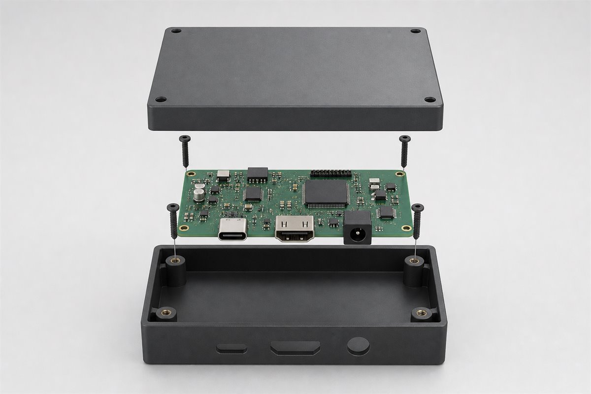
Checking connectors against the panel before production helps you avoid blocked ports, hidden LEDs and switches that bind. A PCB can fit inside the housing while its USB connector sits too high or its button requires side force. The final position depends on the complete tolerance chain: PCB outline, mounting holes, standoff height, connector placement, solder joints, panel thickness and cutout tolerance.
Check every user or cable interface in the assembled condition:
- connector centerline relative to the enclosure datum;
- cutout width, height, corner radius and panel thickness;
- component body and mating-plug clearance;
- insertion direction and room for the cable bend;
- LED, button, display or sensor viewing/access angle;
- allowed connector overhang from the PCB edge;
- mechanical support for connectors exposed to repeated force.
Use the component manufacturer’s drawing and the approved 3D model where available; a silkscreen outline and centroid file are not complete mechanical definitions. For early builds, inspect the PCBA in a real or dimensionally representative housing. If a connector works only when the board is pushed sideways, correct the interface before production instead of accepting a fragile workaround.
What Component Clearance Is Needed Inside a PCB Enclosure?
Verifying the full component envelope helps you avoid cracked parts, pinched cables and covers that will not close. Check height as well as distance from the walls: capacitors, transformers, heat sinks, relays, connectors and through-hole leads can interfere with the cover, fasteners, ribs or cables. BOM or library height alone may miss soldering, lead forming, adhesive, insulation, thermal pads and component tolerances.
Build a clearance review around actual assembly risks:
- maximum component height on both PCB sides;
- enclosure ribs, bosses, screws and lid features above the PCB;
- solder-joint and through-hole lead clearance below the PCB;
- copper keep-out around conductive mechanical hardware;
- spacing needed for hand insertion, cable routing and rework;
- movement caused by vibration, cable force or flexible parts;
- access required for programming and test points.
Use correct component models and released revisions for the CAD interference check. For critical areas, add a dimensioned note or keep-out instead of relying on a model that may have the right footprint but the wrong height. Also check service access. Defining cable and PCB removal steps before production lets the supplier quote the real labor and tooling instead of discovering extra work on the line.
How Should Grounding, Shielding and Heat Transfer Be Coordinated?
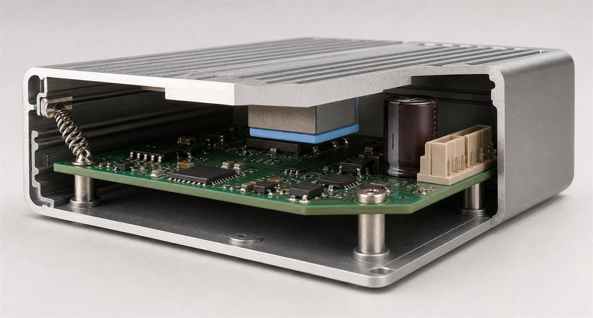
Clear grounding, shielding and thermal interfaces help your team avoid intermittent contact, ineffective shielding and thermal pads that never touch. Because these functions cross the PCB–enclosure boundary, your electrical, mechanical and thermal teams should define them as buildable details.
Identify intentional electrical contact points in the drawings. Paint or anodizing may block contact unless the finish is controlled; spring fingers, conductive gaskets, plated holes and metal hardware also need space and an approved assembly method. For heat transfer, control component height, pad thickness and compression, enclosure flatness and fastener sequence. A thermal pad cannot compensate for an unknown gap, and the supplier should not choose a thermal solution without your approval.
Coordinate these items before requesting production:
- ground and chassis connection points;
- copper and solder-mask treatment around contacts;
- coating or finish exclusions on the enclosure;
- shielding gasket, clip or spring-finger locations;
- heat-producing component location and allowable temperature;
- thermal-interface material and installed thickness;
- inspection or continuity checks required after assembly.
When high-speed or controlled-impedance signals are involved, enclosure integration does not remove the need for a released PCB construction. Review the PCB stack-up and impedance control guidelines before routing and fabrication.
What Should You Check Before PCB Enclosure Assembly?
Finding a mismatch before the first production lot protects your schedule and avoids paying for parts that cannot be assembled. Compare the PCB fabrication package, assembly package and enclosure documentation together instead of approving each file set in isolation.
Use this pre-assembly gate:
- Confirm that the PCB, BOM, CPL, assembly drawing and enclosure drawing use the same revision.
- Compare the PCB outline and mounting coordinates against the mechanical datum.
- Review connector, indicator, switch and display alignment.
- Check top-side and bottom-side component envelopes.
- Confirm fasteners, washers, standoffs and insulating parts.
- Identify intentional grounding, shielding and thermal interfaces.
- Define the assembly sequence and cable-routing order.
- Agree on inspection, programming and functional-test responsibilities.
- Build and approve a representative sample before scaling the quantity.
A realistic fit-check example. An industrial controller PCBA fits the enclosure cavity, but its panel connector is slightly low after the board is tightened to four standoffs. Enlarging the panel opening would hide the immediate problem but could weaken sealing and leave an inconsistent gap. The useful response is to inspect the complete tolerance chain: PCB mounting coordinates, standoff height, connector placement, panel cutout and assembly sequence. The customer then approves the correct drawing or layout change before repeat production.
This review turns “does not fit” into a specific, solvable engineering question and prevents an unauthorized PCB or enclosure modification from becoming an undocumented production workaround.
When the requested scope goes beyond the PCBA and includes enclosure installation, wiring, labels or final testing, define it as a box build PCB assembly project rather than assuming those tasks are included in a normal PCBA quotation.
What Files Make a PCB Enclosure RFQ Faster and More Accurate?
A complete RFQ helps you receive a more accurate price, fewer engineering questions and a clearer delivery plan. The supplier needs both the board requirements and assembly interfaces; a Gerber file and enclosure photo leave too many assumptions.
For PCB fabrication and PCBA, provide:
- Gerber or ODB++ fabrication data;
- NC drill data and fabrication drawing;
- BOM with approved manufacturer part numbers and sourcing rules;
- centroid or component-placement file;
- assembly drawing and special workmanship notes;
- quantity, build stage and required delivery schedule;
- inspection, programming and test requirements.
For enclosure integration, also provide:
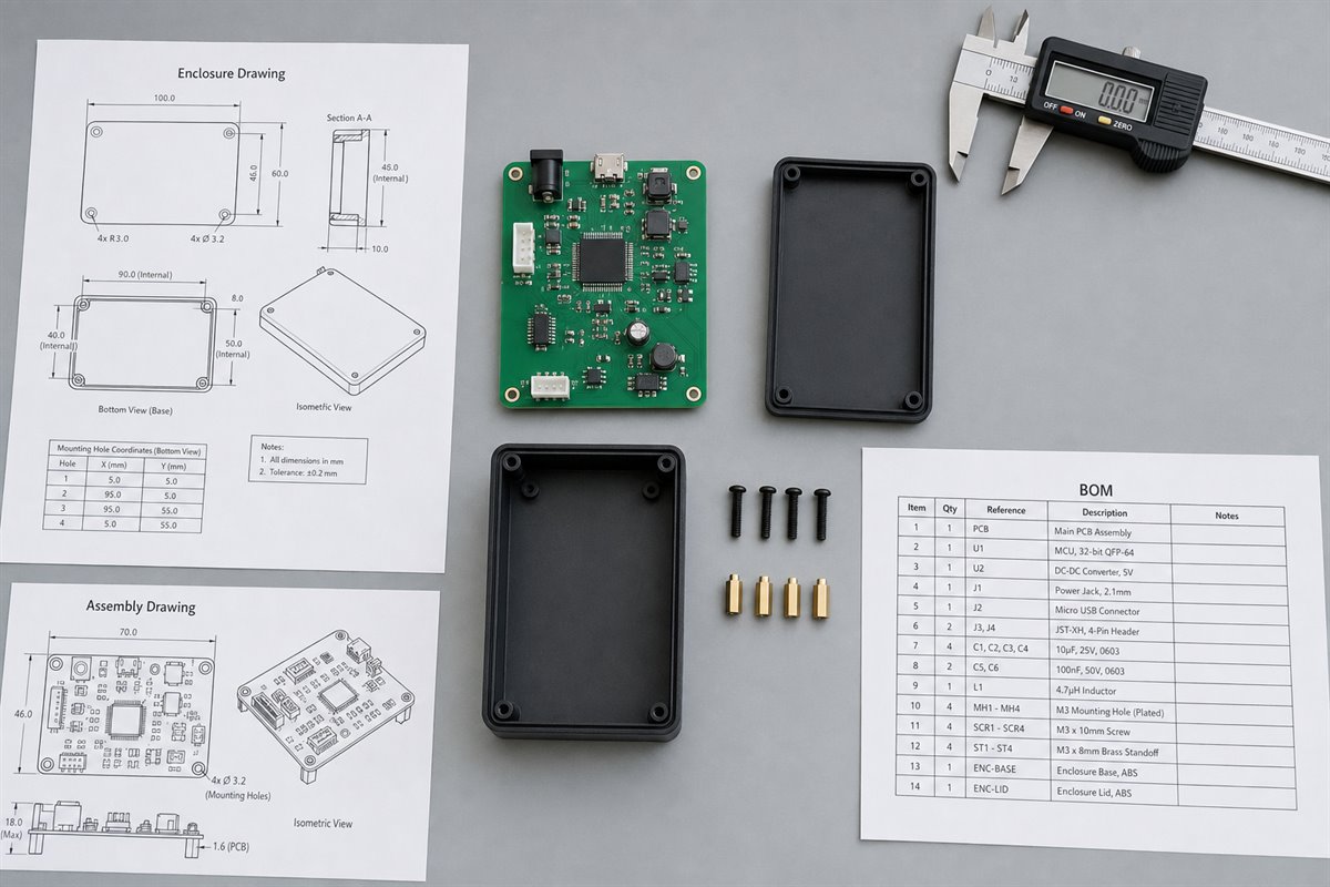
- dimensioned enclosure drawing and available 3D model;
- PCB mounting datum, standoff and fastener information;
- connector and panel-cutout details;
- cable, harness and wiring drawings where applicable;
- grounding, shielding and thermal-interface instructions;
- labels, hardware and customer-supplied parts list;
- approved sample or acceptance criteria.
State which parts you will supply and which parts need sourcing. If alternates are allowed, define who approves them. A photograph can explain the product, but controlled drawings and released files are what make the quote and production plan repeatable.
For a combined board and assembly quotation, the PCB manufacturing and assembly RFQ guide provides a broader file checklist.
FAQs About PCB Enclosures
What is the main purpose of a PCB enclosure?
It protects and supports the PCB or PCBA while providing the mechanical interfaces required by the product. Depending on the approved design, it may also contribute to grounding, shielding, environmental protection and heat transfer.
How do I know whether a PCB will fit an enclosure?
Compare the released PCB outline, mounting-hole coordinates, component envelopes and connector locations with the enclosure’s usable internal dimensions, standoffs, ribs and cutouts. Include manufacturing and assembly tolerances rather than checking only nominal dimensions.
Should I choose the enclosure or design the PCB first?
Either sequence can work, but the interfaces must be coordinated early. A standard enclosure may constrain the PCB outline and connector positions. A custom enclosure may be developed around the PCBA. In both cases, control the same datums and revisions before production.
Can a PCB manufacturer design the complete enclosure for me?
Do not assume this is included. Full industrial and mechanical enclosure design is a separate discipline. EBest Circuit (Best Technology) can review PCB manufacturability, fabricate the PCB, support BOM sourcing and PCBA, and assist with agreed enclosure integration and testing according to customer-released drawings and requirements.
What should I send for a PCB enclosure assembly quotation?
Send the PCB fabrication files, BOM, placement data, assembly drawing, enclosure drawing or 3D model, mounting and cutout details, wiring information, test requirements, quantity and approved assembly instructions.
If you need PCB fabrication, component sourcing, PCBA and an enclosure-fit review based on released mechanical files, send the package to sales@bestpcbs.com. EBest Circuit (Best Technology) will identify missing manufacturing information and clarify the assembly scope, so you can resolve fit risks before they become production rework. A complete PCB enclosure package also gives both teams a clearer basis for quotation and sample approval.