

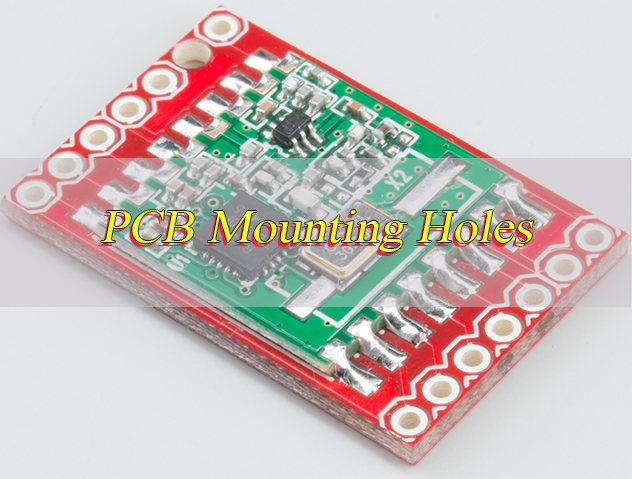
What are PCB mounting holes and how do you design them correctly? These essential structural components secure your PCB to enclosures. Getting their design right avoids reworks and ensures durability. This guide breaks down everything you need to know about PCB mounting holes, including sizes, placement and tool usage.
What Are Mounting Holes in PCB?
Mounting holes on PCB (also called mounting holes pcb) are non-conductive or conductive holes drilled into the PCB substrate for mechanical fastening. Unlike vias used for electrical connections between PCB layers, mounting holes primarily serve a structural purpose. They allow screws, bolts, or standoffs to secure the PCB to a chassis or enclosure.
There are two main types of mounting holes in PCB: Non-plated through holes (NPTH) for pure mechanical fastening and Plated through holes (PTH) that can double as grounding points.
Every PCB design requires carefully planned mounting holes. This includes consumer electronics and industrial control boards. Proper planning keeps the board stable during operation and prevents component damage or signal interference.
What Size Are PCB Mounting Holes?
PCB mounting hole size is determined by the fastener (screw/bolt) you plan to use. A general rule applies: the hole diameter should be 0.1–0.2mm larger than the fastener’s nominal diameter. This accounts for manufacturing tolerances and ensures easy assembly.
Using the wrong size causes problems. A too-small hole makes installation impossible, while a too-large hole leads to PCB wobble. Below is a detailed PCB mounting hole size chart for the most common fastener sizes.
| Fastener Size (Metric) | Recommended PCB Mounting Hole Size (mm) | Recommended Pad Diameter (mm) (for Plated Holes) | Common Application |
| M2 | 2.1–2.2 | 4.0–4.5 | Small consumer electronics (wearables, smartphones) |
| M2.5 | 2.6–2.7 | 4.5–5.0 | Tablets, small IoT devices |
| M3 | 3.1–3.2 | 5.0–6.0 | Industrial PCBs, Arduino boards, power supplies |
| M4 | 4.2–4.3 | 6.5–7.0 | Large industrial boards, automotive PCBs |
| M5 | 5.2–5.3 | 8.0–8.5 | Heavy-duty equipment, industrial control panels |
For non-standard fasteners, calculate the PCB mounting hole size by adding 0.1–0.2mm to the fastener’s diameter. A 1.5mm screw requires a 1.6–1.7mm mounting hole.
Confirm your PCB manufacturer’s capabilities. Many factories have a minimum hole size limit, typically 0.8mm for mechanical drilling.
What Is the Spacing for PCB Mounting Holes?
PCB mounting hole spacing refers to the distance between the centers of two mounting holes. It must match the fastener spacing of your enclosure or bracket.
Maintain consistent spacing between all holes when using multiple fasteners. This ensures even weight distribution across the PCB.
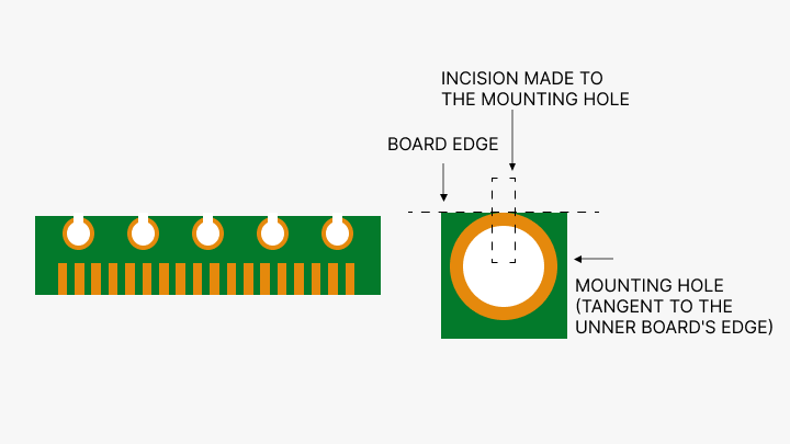
Ensure a minimum edge distance of 1.5–2mm between the hole edge and the PCB edge to prevent board cracking.
Keep a 3mm minimum distance between mounting holes and components or high-speed traces to avoid interference.
For rectangular PCBs, space holes symmetrically along the board’s edges. For circular PCBs, space holes evenly around the circumference, such as three holes spaced 120° apart.
Use a ruler or design software to measure spacing accurately. Even a 0.1mm error can cause misalignment.
Where to Place Mounting Holes on PCB?
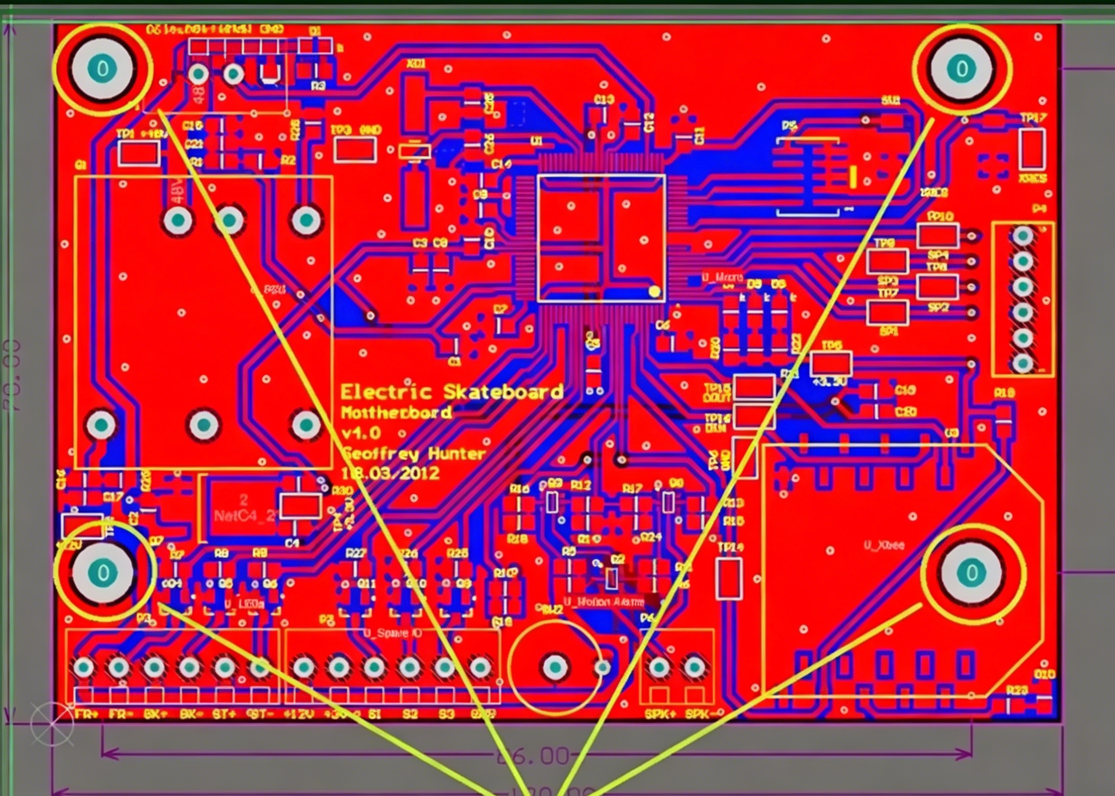
Knowing where to place mounting holes ensures PCB stability and avoids component damage. The golden rule is to place holes symmetrically around the PCB’s center of mass for even weight distribution.
Follow these 5 key guidelines for proper placement:
- Prioritize corner placement: Place mounting holes near the four corners of rectangular PCBs. This provides the best stability and prevents board flexing. Small PCBs (less than 50mm x 50mm) can use 2–3 holes instead of four.
- Avoid component interference: Keep holes 3mm away from surface-mount components, through-hole components and high-speed traces. This prevents damage during installation and avoids signal interference.
- Align with mechanical structures: Match hole positions to the enclosure’s fastener points. Use mechanical design files to confirm spacing and coordinates for a secure fit.
- Add extra holes for heavy components: If your PCB has heavy components like transformers, add additional mounting holes near these components to support their weight.
- Maintain edge clearance: Keep holes 1.5–2mm away from the PCB edge to prevent the board from cracking during drilling or assembly.
A standard Arduino PCB provides a practical example. Its four mounting holes are placed near the corners, aligned with standard brackets to keep the board stable while leaving space for components.
Should PCB Mounting Holes Be Grounded?
PCB mounting holes do not need grounding in all cases. The decision depends on your application and electromagnetic interference (EMI) requirements.
Use plated through holes (PTH) if you need to ground mounting holes. These connect to the PCB’s ground plane and the enclosure via a conductive fastener, creating a Faraday cage to block external noise.
Use non-plated through holes (NPTH) for pure mechanical fastening. These do not connect to the ground net and avoid accidental short circuits.
Never connect grounded mounting holes to power nets. Always run a design rule check (DRC) to confirm correct ground connections.
How to Drill Mounting Holes in PCB?
- Drilling mounting holes requires precision to avoid board or component damage. Follow these sequential steps:
- Mark hole positions accurately: Use your PCB design file to print a template or mark positions directly on the PCB with a marker. Confirm coordinates match the enclosure’s fastener points.
- Secure the PCB firmly: Clamp the PCB to a flat surface. Place a piece of scrap wood under the PCB to protect the drill bit and prevent board splintering.
- Select the correct drill bit: Use a carbide-tipped drill bit matching your desired hole size. Use a micro drill bit for holes smaller than 1mm and a standard twist drill bit for larger holes.
- Set the correct drilling speed: Use a drill press set to 10,000–15,000 RPM for FR-4 PCBs. Too slow a speed can bind the bit, while too fast can overheat the board.
- Deburr holes after drilling: Use a deburring tool or sandpaper to remove sharp edges. This prevents wire or component damage during assembly.
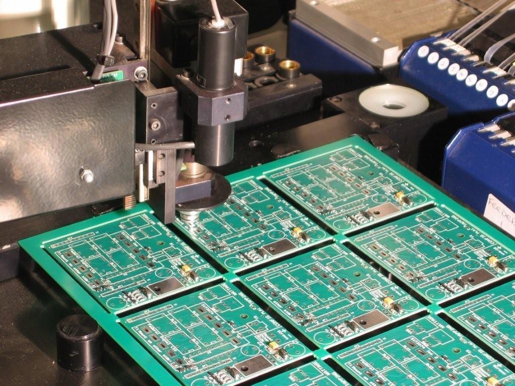
- Follow mass production guidelines: For large-scale production, provide manufacturers with a detailed drill file (e.g., Gerber file) to ensure consistent hole placement and size.
How to Make Mounting Holes in Common PCB Design Tools?
Creating mounting holes in popular PCB design tools is simple. Below are step-by-step guides for common tools, covering altium pcb mounting holes, kicad pcb mounting holes, cadence pcb designer mounting holes, solidworks pcb mounting holes, and ultiboard pcb mounting holes.
Altium PCB (Altium PCB Mounting Holes)
- Open your PCB design.
- Go to “Place” and select “Pad” or use the shortcut P + P.
- In pad properties, set “Layer” to “Multi-Layer” for plated holes or “Mechanical 1” for non-plated holes.
- Set “Hole Size” to your desired diameter.
- For plated holes, set “Pad Size” to 1.5–2x the hole size.
- Place the pad at your desired position and repeat for additional holes.
- For non-plated holes, set the pad’s “Net” to“No Net” to avoid DRC errors.
KiCad (KiCad PCB Mounting Holes)
- Open the PCB Editor.
- Go to “Place” and select “Pad” or use the shortcut P.
- In the pad dialog, select “Through Hole” as the type.
- Enter the hole size and pad size (1.5x the hole size for plated holes).
- Uncheck “Plated” for non-plated holes.
- Place the pad at the desired coordinates and repeat for other holes.
- Use the “Measure” tool to confirm spacing and edge clearance.
Cadence PCB Designer (Mounting Holes Cadence PCB Designer)
- Open your PCB design in Allegro (Cadence’s PCB tool).
- Go to “Place” and select “Pad” or use the shortcut P.
- In the pad editor, set “Hole Type” to “Through” and enter the hole size.
- Set “Pad Stack” to “Plated” for grounded holes or “Non-Plated” for mechanical-only holes.
- Set the pad diameter to 1.5–2x the hole size.
- Place the pad using the “Grid” tool for precision and repeat as needed.
- Connect plated holes to the ground net if required.
SolidWorks PCB (SolidWorks PCB Mounting Holes)
- Open your SolidWorks PCB design.
- Go to “PCB” and select “Place” then “Pad”.
- In pad properties, set “Layer” to “Multi-Layer” and enter the hole size.
- Set “Plated” to “Yes” for plated holes or “No” for non-plated holes.
- Place the pad at the desired position, aligning with your mechanical assembly.
- Use “Smart Dimension” to set spacing between holes and edge clearance.
Ultiboard (Ultiboard PCB Mounting Holes)
- Open your Ultiboard project.
- Go to “Place” and select “Pad” or use the shortcut P.
- In pad properties, set “Hole Size” to your desired diameter.
- Set “Plated” to “True” for plated holes or “False” for non-plated holes.
- Set the pad diameter to 1.5x the hole size.
- Place the pad using the “Snap to Grid” feature for accuracy.
- Save your design and run a DRC to check for errors.
How to Use Vias with PCB Mounting Holes Properly?
PCB mounting holes with vias improve grounding and mechanical strength. Vias are small conductive holes that connect the mounting hole’s pad to inner ground planes.
Follow these steps to use vias with mounting holes:
- Choose the right via size: Use 0.3–0.5mm vias, compatible with most PCB manufacturers.
- Place vias symmetrically: Add 4–6 vias around the mounting hole’s pad, spaced evenly at 90° intervals.
- Connect vias to the ground net: Ensure all vias link to the PCB’s ground plane, not power nets.
- Maintain clearance: Keep vias 0.5mm away from the mounting hole edge to prevent drill bit damage.
Vias with mounting holes are ideal for high-noise environments like industrial or automotive applications. They reduce EMI and distribute mechanical stress to prevent board cracking.
FAQs About PCB Mounting Holes
Q1: What is the standard PCB mounting hole size for M3 screws?
A1: The standard PCB mounting hole size for M3 screws is 3.1–3.2mm. This size accounts for manufacturing tolerances and ensures a secure fit. Plated holes should use a 5.0–6.0mm pad diameter.
Q2: Where to place mounting holes on PCB for maximum stability?
A2: Place mounting holes symmetrically near the PCB’s four corners. This distributes weight evenly and prevents flexing. Smaller PCBs can use 2–3 holes near the center of mass.
Q3: Should consumer electronics PCB mounting holes be grounded?
A3: Grounding is unnecessary for low-EMI consumer devices like basic wearables. Use non-plated holes (NPTH) for mechanical fastening. Ground plated holes (PTH) only for high-EMI devices like smartphones or IoT modules.
Q4: How to drill PCB mounting holes without damaging components?
A4: Mark positions accurately, secure the PCB firmly, use a carbide-tipped drill bit, and drill at 10,000–15,000 RPM. Deburr holes after drilling and cover soldered components to avoid debris damage.
Q5: Can I use vias with PCB mounting holes for better grounding?
A5: Yes. Add 4–6 small vias (0.3–0.5mm) around the mounting hole’s pad and connect them to the ground plane. This improves grounding and reduces EMI.
Q6: What is the minimum PCB mounting hole spacing?
A6: The minimum center-to-center spacing is 5mm for standard FR-4 PCBs. Larger holes (≥3mm) require 8–10mm spacing to maintain mechanical strength. Edge-to-hole distance should be at least 1.5mm.
Q7: How to make mounting holes in KiCad PCB Designer?
A7: Open the PCB Editor, go to “Place” then “Pad”, select “Through Hole”, enter the hole and pad size, uncheck “Plated” for NPTH, and place the pad at the desired position. Use the “Measure” tool to confirm spacing.
You may also like


Tags: PCB mounting hole design, PCB mounting hole placement, PCB mounting hole size, PCB mounting holes