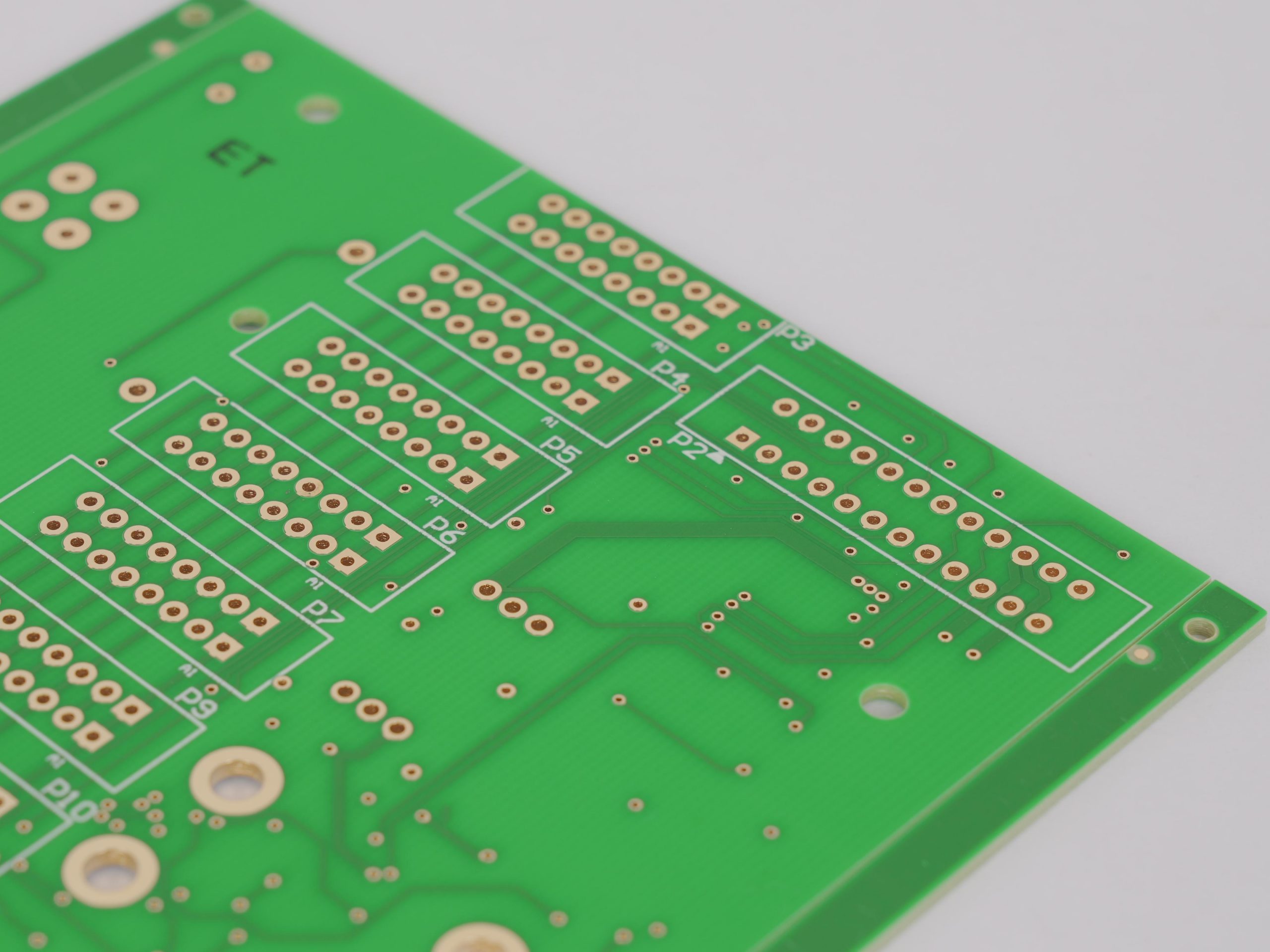
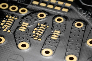
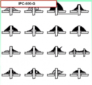
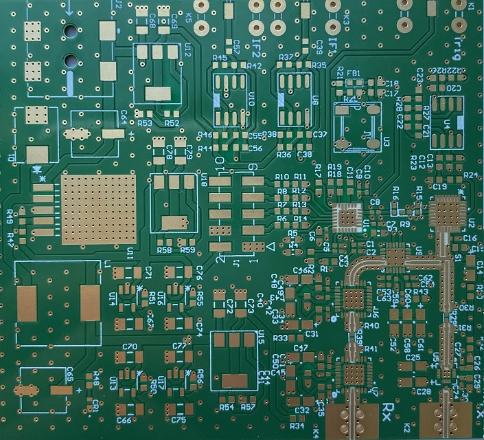
PCB (Printed Circuit Board) boards can be classified according to their constituent materials and characteristics. PCBs are classified into single-sided boards, double-sided boards, and multi-layer boards according to board applications. They are classified into flexible PCB boards (flexible boards), rigid PCB boards, rigid-flexible PCB boards (rigid-flexible boards) according to materials, etc.
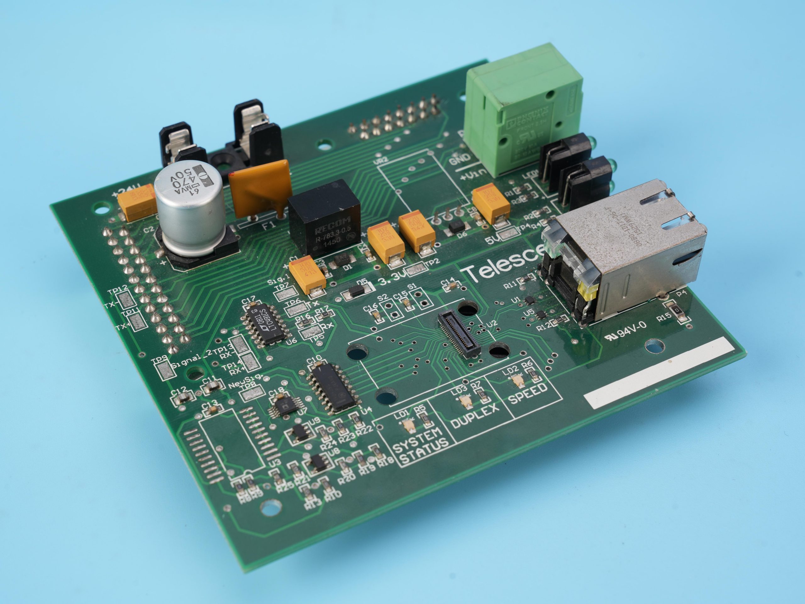
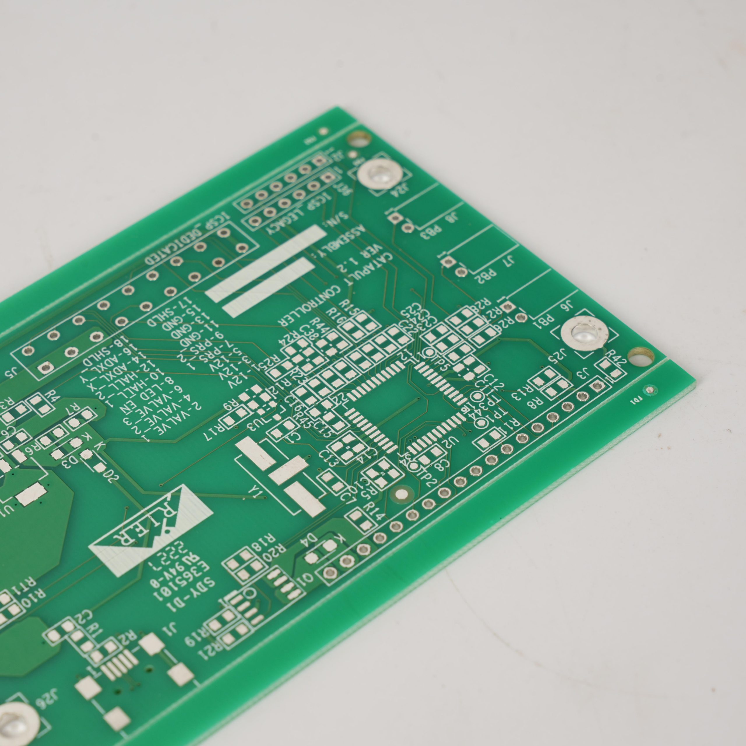
PCB is an important electronic component, a support for electronic components, and a provider of electrical connections for electronic components. Since it is made using electronic printing technology, it is also called a printed circuit board. PCB is simply a thin board with integrated circuits and other electronic components.
1. Single-sided board:
On the most basic printed circuit board, parts are concentrated on one side and wires are concentrated on the other side. Because wires only appear on one side, this type of printed circuit board is called a single-sided board. Because single-sided boards have many strict restrictions on designing circuits (because there is only one side, wiring cannot cross and must go around a separate path), early circuits used this type of circuit board.
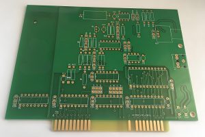
2. Double-sided board
This type of circuit board has wiring on both sides. In order to connect the wires on both sides, there must be a proper circuit connection between the two sides. This connection between the circuits is called a guide hole. A guide hole is a small hole filled or coated with metal on a printed circuit board, which can be connected to the wires on both sides. Because the area of a double-sided board is doubled that of a single-sided board, and the wiring can be interlaced (can go around to the other side), double-sided boards can be used on more complex circuits than single-sided boards.
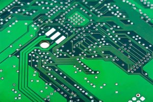
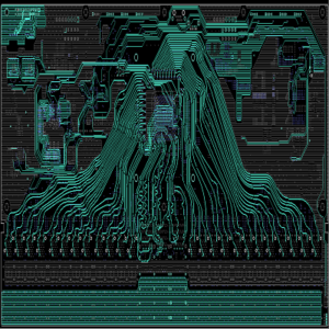
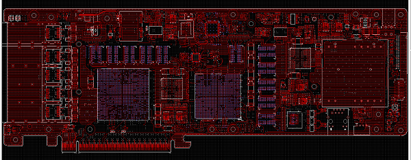
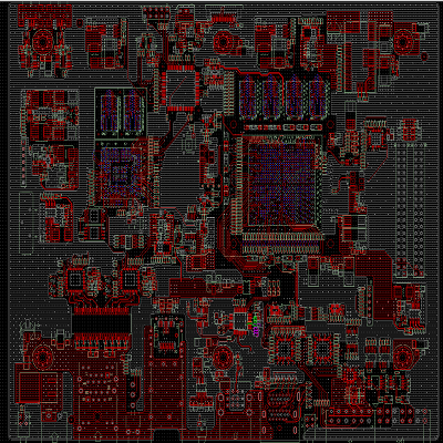
3. Multilayer board:
In order to increase the area that can be wired, multilayer boards use more single- or double-sided wiring boards. Multilayer boards use several double-sided boards, and put an insulating layer between each layer of boards and glue them firmly. The number of layers of the circuit board represents how many independent wiring layers there are, usually an even number of layers, and includes the two outermost layers.
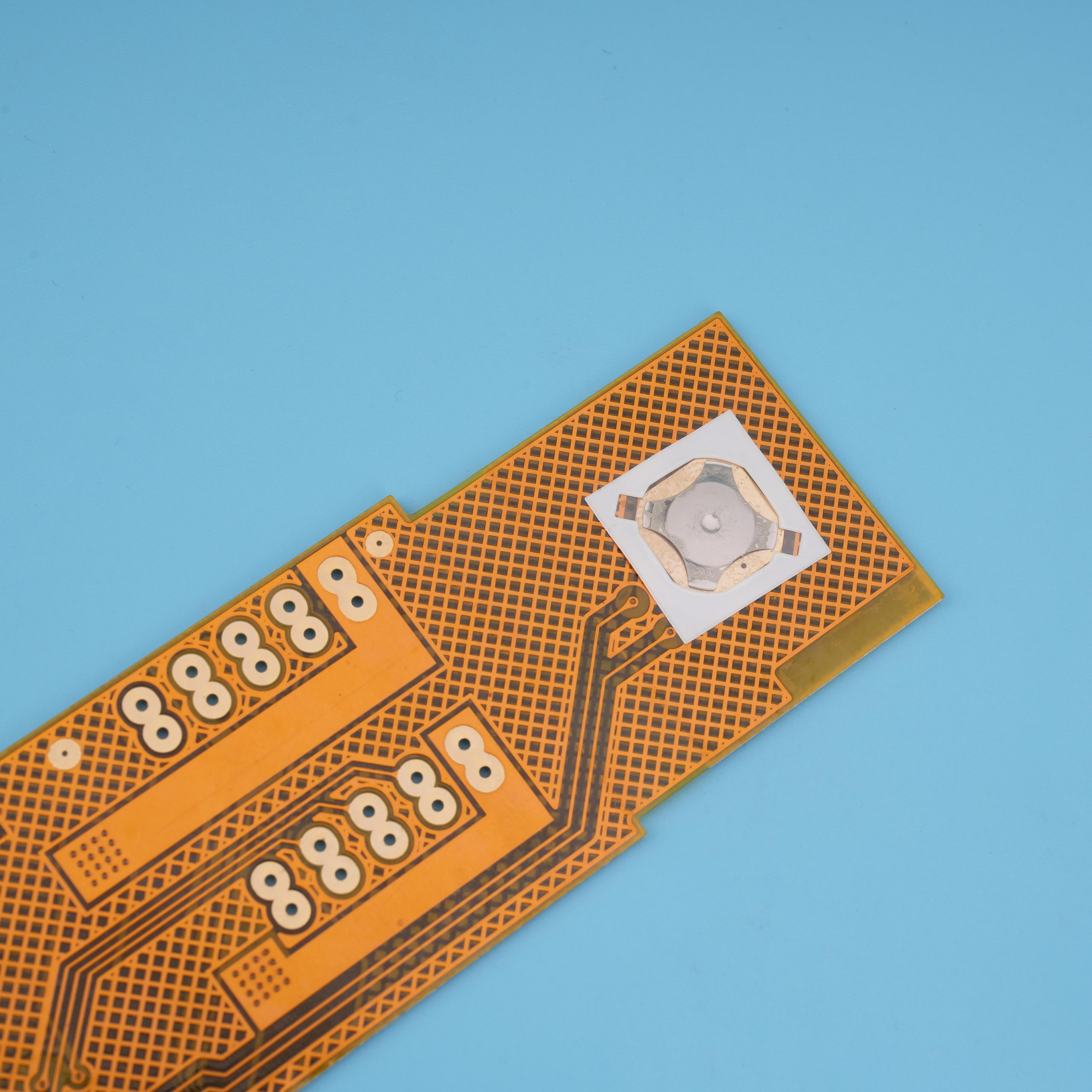
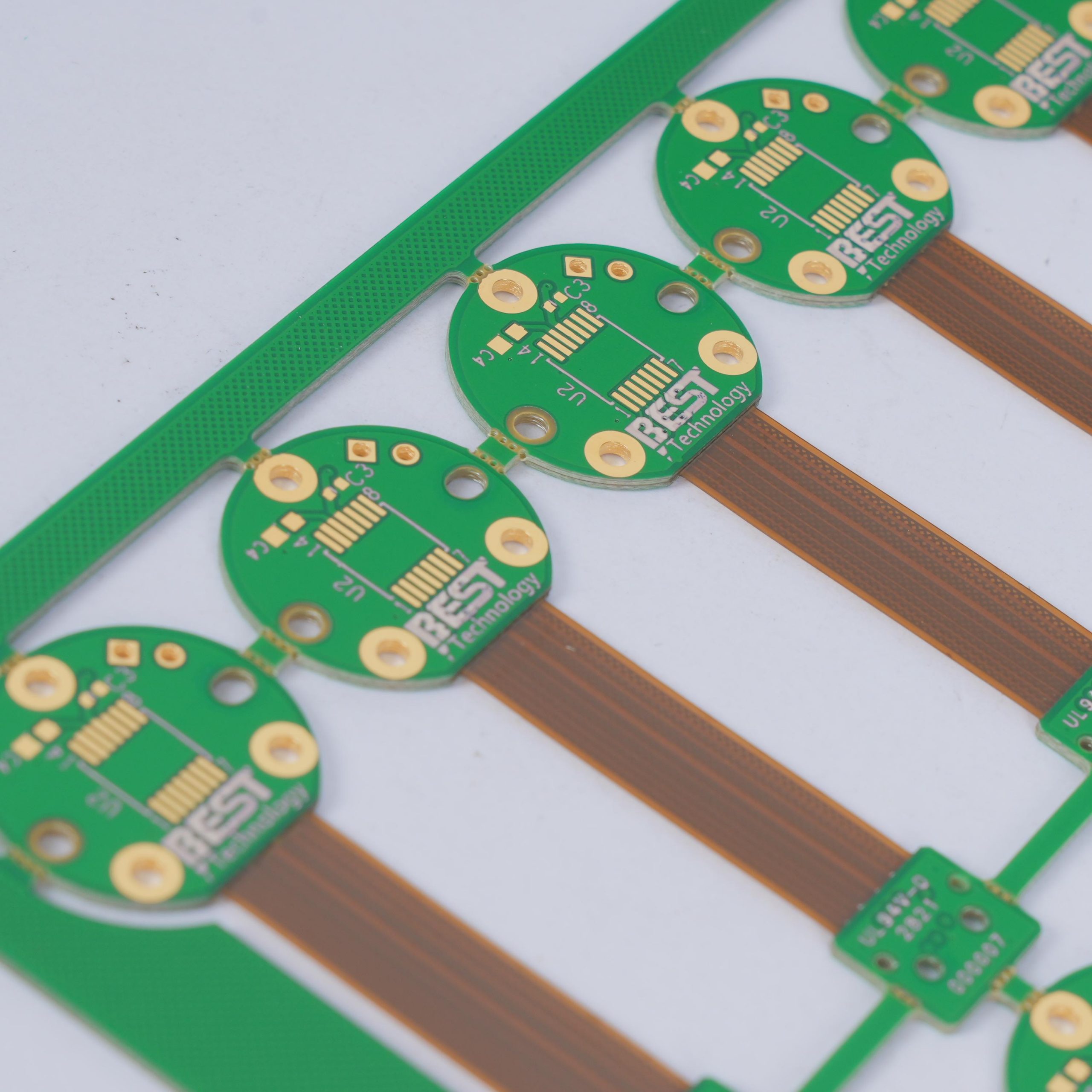
4. Flexible PCB board
Flexible PCB board is a printed circuit board made of a flexible substrate. Its advantage is that it can be bent, which is convenient for the assembly of electrical components. Flexible circuit board, flexible PCB, flexible circuit and multi-function printed circuit are other names for these circuit boards. These printed circuit boards are made using the same components as rigid printed circuit boards. The main difference is that the circuit board is designed to bend to the desired shape throughout the application process. These PCBs are available in single-sided, double-sided, and multi-layer configurations. This helps reduce the complexity of unit assembly.
5. Rigid PCB Board
Rigid PCB is a circuit board that cannot be twisted or folded. The base material of the board is a rigid substrate, which gives the board rigidity and strength. They are composed of multiple layers, including substrate layers, copper layers, solder mask layers, and silk screen layers, which are bonded together by adhesives and heat. While some circuit boards are single-sided, double-sided, or multi-layered, rigid PCBs can be any of these as needed. However, once made, they cannot be modified or changed.
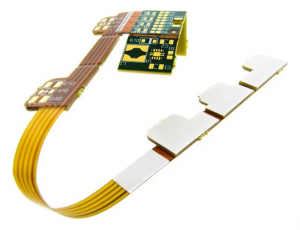
6. Rigid-Flex Board
Rigid-Flex Board is a hybrid circuit board that combines elements of flexible and rigid circuit boards to form a foldable or continuously bendable circuit board, which is usually molded into a curved shape or curve during the manufacturing process.
The flexible portion of the circuit board is often used for interconnections between rigid circuit boards, allowing narrower wires to take up less space, thereby reducing the size of the circuit board. Using flexible PCBs for interconnections often eliminates the need for bulky and heavy connectors, making rigid-flex boards lighter. The design of rigid-flex boards is slightly more complicated because these boards are 3D constructed, allowing the board to be folded or twisted to produce the shape required for the product.
7. High-frequency PCB board
High-frequency circuits refer to the overall circuit board design, not the other types of circuit board structures we described earlier. These PCBs are designed to conduct signals over 1 GHz.
High-frequency boards mostly use FR4-grade glass-reinforced epoxy boards, polyphenylene ether (PPO) resins, and Teflon, but Teflon has a low and stable Dk value, low dielectric loss, low hygroscopicity, and is slightly more expensive.
When designing high-frequency circuits, various factors must be considered, such as Dk value, dissipative loss, and dielectric thickness. The DK value of the substrate is an important factor to remember. Substrates with a higher probability of Dk value changes usually experience impedance changes, which affects the harmonics that make up the electrical signal, resulting in poor signal integrity.
8. Copper substrate
Copper substrate is a metal substrate with high thermal conductivity, suitable for high-frequency circuits and areas with large high and low temperature changes and heat dissipation and architectural decoration industries for precision communication equipment.
The copper substrate circuit layer requires a large current carrying capacity, and a thicker copper foil should be used, with a thickness of generally 35μm~280μm. The thermal conductive insulation layer is the core technology of the copper substrate. It is composed of core thermal conductive components and high molecular polymers, with low thermal resistance (0.15), excellent viscoelastic properties, resistance to thermal aging, and the ability to withstand mechanical and thermal stress.
The copper substrate metal base is the supporting member of the copper substrate, which is required to have high thermal conductivity. It is generally a copper plate, and a copper plate can also be used (where the copper plate can provide better thermal conductivity). It is suitable for conventional mechanical processing such as drilling, punching and cutting.
9. Aluminum-based PCB board
The design of aluminum-based PCB circuits is similar to that of copper-based PCBs, but the substrate material of aluminum-based PCBs is aluminum metal, rather than the standard glass fiber used in most circuits.
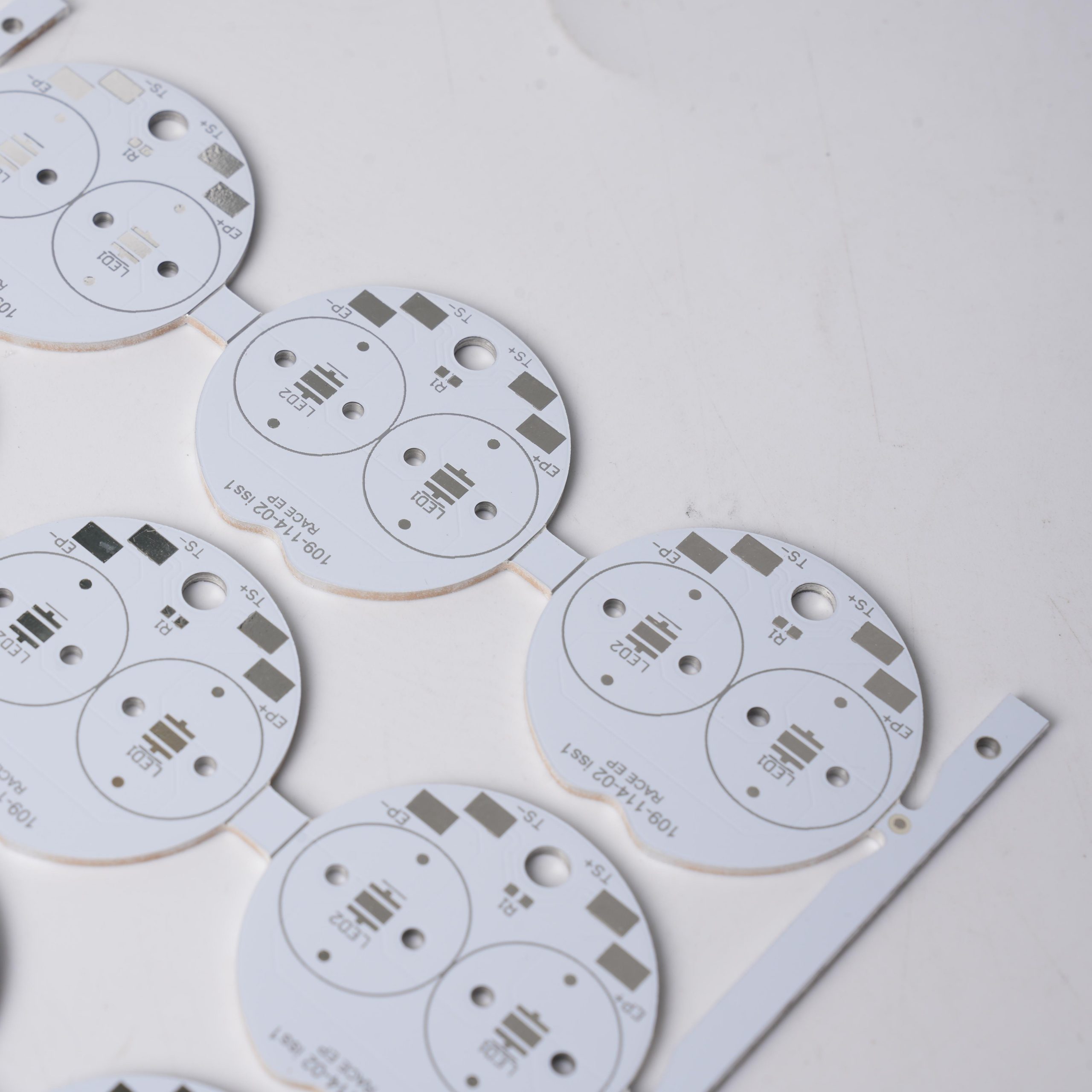
The aluminum layer is reinforced with the least heat-resistant insulation material, which means less heat is transferred from the insulation material to the backing. After applying the insulation layer, another layer of copper is required.
10. High Density Interconnect (HDI) PCB
Among the many types of PCBs, HDI PCB is a circuit with multiple interconnections that takes up very little space. HDI components are mounted close to each other, minimizing PCB space while maintaining high functionality. Boards containing 120-160 pins per square inch are classified as HDI PCBs.
HDI designs integrate dense device mounting and multi-purpose wiring. With the help of microvias, buried vias, and blind vias, compact circuits can be made, minimizing drilling to copper. For the electrical requirements of high-speed signals, HDI PCBs must have high-frequency conduction capabilities, impedance control, and minimal redundant radiation.
11. Thick Copper PCB
Thick copper PCB is also called heavy copper PCB. Basically, it contains more than 2 ounces of copper in the inner and outer layers of the board. Heavy copper transmitters significantly increase the overall thickness of the board; thick copper boards are known for supporting high currents, high temperatures, and cyclical thermal cycles.
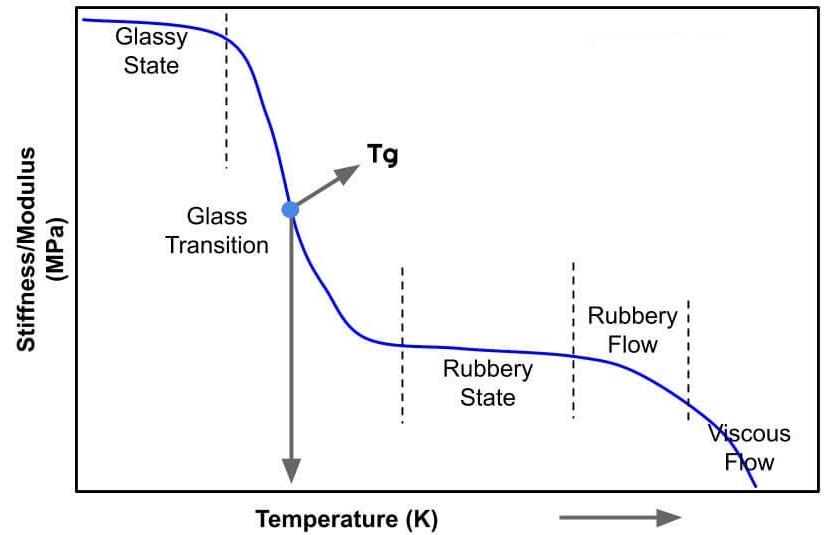
12. High TG PCB
Among various types of PCBs, high Tg PCBs are circuit boards designed to work at high temperatures. Glass transition temperature (Tg) is an essential element of any epoxy resin. It is basically the temperature point at which the polymer changes from a hard glass substrate to a soft rubber substrate. The substrates used to make high Tg circuit boards must be flame retardant, which means that they soften instead of burning at the glass transition point (Tg).
The higher the Tg value, the higher the temperature requirement during lamination. Under such conditions, the PCB will become hard and brittle, affecting the aperture size and related electrical properties. Standard boards will soften, deform and melt under such conditions, and their mechanical and electrical properties will be significantly reduced.
Standard FR-4 Tg is between 130-1400C, medium Tg is between 150-1600C, and high Tg is above 1700C. The higher the Tg value, the better the board’s heat, moisture and chemical resistance.
Conclusion:
PCB board types are updated and iterated with the rapid development of the industry, and various types of PCB boards have gradually evolved to cope with various application scenarios, adding corresponding materials according to the required performance. BEST Technology has various PCB types of manufacturing technology, which can meet your any type of PCB needs.