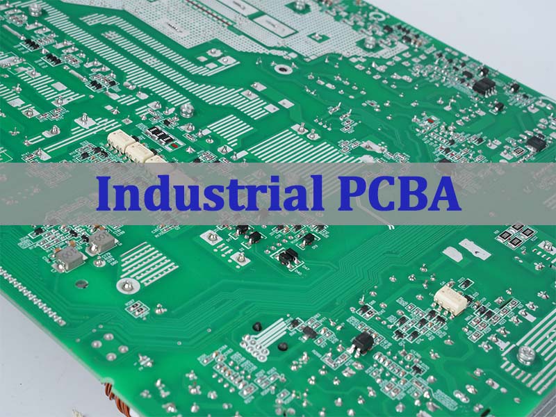
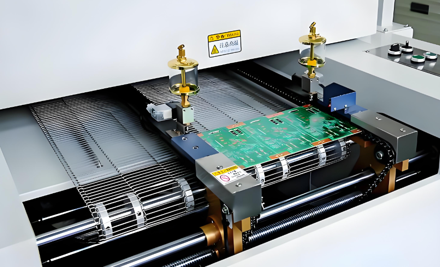
High current PCB design is a critical skill for modern electronics. This guide walks you through creating robust, safe, and reliable boards that handle significant power without a hitch.
Many engineers face real high current PCB problems. Common struggles include:
- Unexpected Failures: Boards that suddenly stop working, often at the worst possible moment.
- Dangerous Overheating: Components or traces getting hot enough to cause damage or become a safety hazard.
- Voltage Drops: The board receives power, but critical components don’t get the voltage they need to function correctly.
- Costly Rework: Discovering a flaw after production, leading to expensive fixes and delays.
- Reliability Questions: A lingering doubt about whether the product will hold up in the field over time.
The good news is that these challenges have solid high current PCB solutions.
- Proactive Analysis and Robust Construction to Prevent Failures.
- Strategic Thermal Management by Design to Combat Overheating.
- Precision Engineering for Power Integrity to Eliminate Voltage Drops.
- Early Collaboration and Design Partnership to Avoid Costly Rework.
- Certified Processes and Real-World Validation to Ensure Reliability.
With over 19 years of specialized experience, EBest Circuit (Best Technology) is a trusted one-stop manufacturer focusing on advanced boards like heavy copper PCBs (up to 20oz), metal core PCBs (MCPCBs), and ceramic PCBs—all essential for robust power applications. Our expertise ensures your design is not just manufacturable, but optimized for performance and durability. We support you from PCB design and prototyping to full turnkey assembly, providing expert DFM feedback and rigorous quality control certified under ISO 9001, ISO 13485, IATF 16949, and AS9100D standards. If you have a project in hand, pls contact our engineering sales team at sales@bestpcbs.com for a prompt and professional consultation.
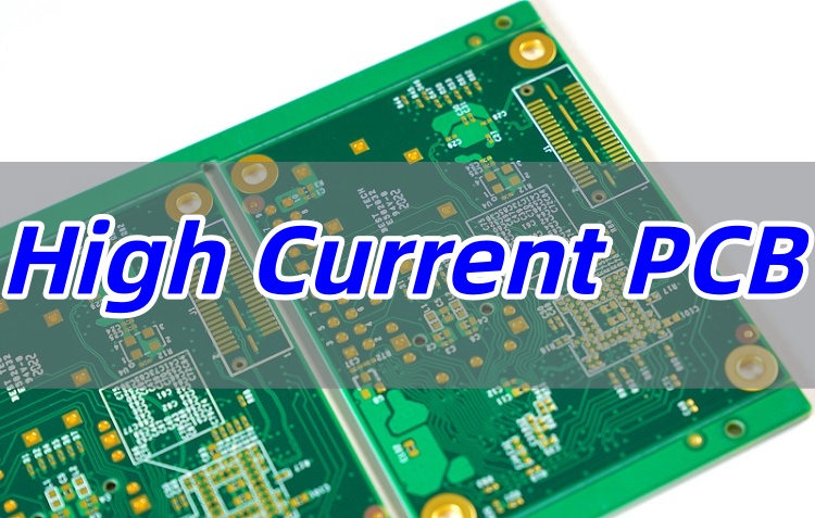
What is a High Current PCB?
Simply put, a high current PCB is a circuit board designed to carry large amounts of electrical current. We are not talking about simple signal traces here. These are boards for serious jobs like electric vehicle controllers, industrial motor drives, or high-power battery systems.
The core purpose is to move energy efficiently and safely from one point to another with minimal loss. The entire design philosophy shifts from simple connectivity to robust power management.
High current PCBs are typically categorized based on their construction and material used to handle the increased thermal and electrical loads:
- Heavy Copper PCBs: These boards use significantly thicker copper layers (typically 3 oz/ft² to 20 oz/ft² or more) for the conductive traces and planes, providing a larger cross-sectional area to carry higher currents and dissipate heat.
- Metal Core PCBs (MCPCBs): Often used for LED lighting and power converters, these boards incorporate a metal substrate (usually aluminum) that acts as a built-in heatsink, offering excellent thermal management.
- Ceramic PCBs: Utilizing substrates like aluminum oxide or aluminum nitride, these boards offer exceptional thermal conductivity and electrical insulation, making them ideal for high-power, high-frequency applications.
- Thick Film Hybrid PCBs: These specialized circuits use screen-printed conductive pastes on a ceramic substrate, capable of withstanding high power densities and stable performance in harsh environments.
In high current PCBs, every millimeter of copper and every component choice carries significant weight.
What Makes a High Current PCB Different from Standard Boards?
Standard PCBs are like the quiet residential streets of the electronics world. High current PCB designs, however, are the major highways handling heavy traffic. The differences are substantial.
- Copper is King: The most obvious difference is the use of heavy copper. Standard boards might use 1oz or 2oz copper. A heavy copper PCB can use 4oz, 10oz, or even more. This provides a much wider “pipe” for current to flow through.
- Trace Geometry: PCB high current traces are wide and thick. There are no delicate lines. The focus is on cross-sectional area to reduce resistance.
- Thermal Management: Heat is the enemy. These boards are built to manage heat effectively. This often means integrated heat sinks, thermal vias, and sometimes even metal cores.
- Component Specs: Every part, especially the high current PCB connector and high current PCB terminal, is chosen for its power rating. A standard header won’t survive here.
- Design Priority: The primary goal is current capacity and thermal performance. Signal integrity, while important, often takes a secondary role in the power sections.
Understanding these differences is the first step toward a successful high current PCB design.
How Important Are PCB High Current Traces on Heavy Copper PCB?
PCB high current traces are the lifelines of your board. Their importance cannot be overstated. On a heavy copper PCB, these traces do the heavy lifting.
Think of a trace as a wire.
- A thin wire has high resistance.
- When high current flows, it generates heat (I²R loss).
- Too much heat damages the board and components.
- A wide, thick trace has very low resistance. It allows current to pass with minimal heat generation.
Furthermore, proper traces prevent voltage drops. If a trace is too thin, the voltage at the end will be lower than at the source. This can cause components to malfunction. For sensitive power applications, stable voltage is non-negotiable.
In short, the traces are not just connections. They are critical functional elements. Getting the PCB high current traces right is perhaps the single most important task in designing high current PCB projects. It directly impacts efficiency, safety, and longevity.
How to Get High Current Traces on PCB?
So, how do you create these robust pathways? It is not just about drawing a wider line in your CAD software. Here is a practical approach:
- Maximize Width: This is the easiest and most effective method. Always make power traces as wide as your board space allows.
- Use External Layers: Routing traces on the outer layers is best. They have direct air exposure, which helps with cooling. Internal traces trap heat.
- Embrace Heavy Copper: The foundation is using a thicker copper weight. Starting with 3oz or 4oz copper gives you a major advantage over standard 1oz boards.
- Remove Solder Mask: Expose the copper traces and cover them with solder. Solder is a decent conductor. Adding a thick layer of solder can significantly increase the cross-sectional area of the trace.
- Utilize Polygons: Instead of thin traces, use large copper pours for power planes. This provides an excellent, low-resistance path for current.
These techniques, especially using a heavy copper PCB, are your primary tools for creating effective high current PCB traces.
How to Calculate PCB Trace Width in High Current PCB?
When dealing with high current PCB design, estimating trace width by “feel” is not an option. It must be calculated precisely. The easiest and most reliable way to do this is by using a PCB Trace Width Current Calculator — like the one available on our website.
All you need to do is input three key parameters:
- Current (Amp): The actual current your circuit will carry.
- Copper Thickness (oz): Usually 1oz (35μm), 2oz (70μm), or higher for heavy copper designs.
- Temperature Rise (°C): The acceptable temperature increase, commonly set between 10°C and 30°C.
Once these are entered, the calculator instantly provides:
- Outer layer line width (mm)
- Inner layer line width (mm)
This quick result gives engineers a reliable reference that complies with IPC-2152 standards — the industry benchmark for thermal and current-carrying performance in copper traces.
Understanding the Formula Behind the Calculation
The calculator’s results are derived from the empirical IPC formula:
I = K × (ΔT)^0.44 × (A)^0.75
where:
- I is the allowable current (A)
- K is a correction factor (0.024 for inner layers, 0.048 for outer layers)
- ΔT is the permissible temperature rise (°C)
- A is the cross-sectional area of the copper trace (square mils)
Once the cross-sectional area is determined, the trace width (W) can be calculated as:
W = A / copper thickness (mil)
For example, with a 70 µm copper layer, a 5A current requires approximately 1.2 mm width at a 10°C temperature rise, or about 0.62 mm if the temperature rise is allowed to reach 30°C.
Why Safety Margin Matters
While calculators give accurate theoretical results, real-world conditions introduce variability — manufacturing tolerances, uneven copper plating, and localized heating.
That’s why engineers always add a safety margin.
If your PCB trace width current calculator shows a required width of 5 mm, design it at 6 mm or even 7 mm if space allows. This small adjustment significantly improves thermal stability and extends the PCB’s lifespan.
Practical Notes from Engineering Experience
- For low-current circuits, 10 mil (0.25 mm) traces are typically enough for 1A.
- At 2A, a 0.5 mm trace is recommended.
- For 30A power paths, use at least 6–7 mm width on 2oz copper or increase to 4oz copper for compact layouts.
- Outer layers dissipate heat better than inner layers, allowing slightly narrower traces for the same current.
Ready to calculate your traces? Use our precise [PCB Trace Width Calculator] to get your outer and inner layer widths in seconds. Just enter your Current, Copper Thickness, and Temperature Rise, and the tool will instantly generate the required trace width for both outer and inner layers.
This eliminates guesswork and saves valuable design time, ensuring your high current PCB remains safe, efficient, and fully compliant with engineering standards.
How to Do High Current PCB Design for Power Devices?
High current PCB design requires a holistic mindset. It is more than just traces. Here is a structured approach:
- Plan the Power Path: Before placing anything, sketch the main current path from the input (high current PCB terminal block) to the output. Keep this path as short and direct as possible.
- Select Appropriate Components: Choose parts rated for the job. This includes your high current PCB screw terminal, high current PCB mount connectors, and any high current PCB jumper. Don’t forget capacitors and inductors.
- Prioritize Thermal Management: Use thermal vias under hot components to pull heat to the other side of the board. Consider a metal core for extreme cases.
- Mind the Connections: Solder joints must be robust. Use large pads and ensure good wetting. A weak joint will become a hot spot.
- Simulate and Review: Use thermal simulation tools if available. Have a second engineer review the layout. A fresh set of eyes catches mistakes.
Following these high current PCB design guidelines will set you on the path to a successful board. It is a process that rewards careful planning.
What is the Function of a High Current PCB Connector on PCB?
The high current PCB connector is the gateway for power. Its function is critical. It is the interface between your board and the outside world.
A good connector provides a low-resistance connection. It ensures power gets onto the board efficiently. A poor connector will heat up, creating a fire risk and causing voltage drops.
Types include:
- High current PCB screw terminals for wire attachment
- High current PCB mount connectors for board-to-board links
- The high current PCB terminal block is a common and reliable choice
These components are mission-critical. Never compromise on their quality.
Where to Get High Current PCB Solutions?
For electronic applications requiring high current carrying capacity, specialized PCB solutions are essential to ensure reliability, durability, and optimal performance. EBest Circuit (Best Technology) stands as a premier provider of high current PCB solutions, offering comprehensive manufacturing capabilities backed by 19 years of industry experience.
1. Heavy Copper PCB Expertise
EBest Circuit (Best Technology) specializes in manufacturing heavy copper PCBs with copper thickness ranging from:
- Standard range: 1oz to 5oz (35μm to 175μm)
- Extended range: Up to 20oz (700μm) for extreme current requirements
Our advanced manufacturing processes enable:
- Inner layer copper: 0.5oz to 30oz
- Outer layer copper: 1oz to 30oz
- Minimum line width/space for heavy copper:
- 20/20oz: 74/90mil (standard), 60/80mil (special)
2. Specialized PCB Technologies
We offer multiple solutions for high current applications:
Metal Core PCBs (MCPCB):
- 1-10 layer construction
- Aluminum and copper core options
- Excellent thermal management (thermal conductivity up to 240W/mK)
- Maximum board dimension: 610×1625mm
Ceramic PCBs:
- HTCC/LTCC solutions (4-64 layers)
- DBC/DPC/AMB technologies
- Working temperature range: -50°C to 800°C
- Superior thermal performance (170W/mK for AlN substrates)
3. Advanced Manufacturing Capabilities
Our production facilities feature:
- Monthly capacity: 260,000 square feet (28,900 square meters)
- Quick-turn prototyping with urgent boards shipped within 24 hours
- Strict quality control following ISO 9001:2015, ISO 13485:2016, IATF 16949 standards
- 97% on-time delivery rate
4. Comprehensive Turnkey Services
EBest Circuit (Best Technology) provides complete solutions:
- PCB design and layout support
- Component sourcing
- PCB assembly (including SMT with 0.2mm pitch BGA capability)
- Full box build services
- Testing (functional, ICT, X-RAY, AOI, SPI)
5. Technical Support and Custom Solutions
Our engineering team offers:
- Design for Manufacturing (DFM) analysis
- Thermal management solutions
- Current carrying capacity calculations
In closing, for high current PCB solutions that combine robust construction, thermal efficiency, and reliable performance, EBest Circuit (Best Technology) offers unmatched expertise and manufacturing capabilities. With nearly two decades of experience, state-of-the-art facilities, and a commitment to quality, we provide comprehensive solutions from design to final product assembly.
Whether you need heavy copper PCBs, metal core boards, or specialized ceramic substrates, our team stands ready to deliver solutions tailored to your high current requirements. Pls feel free to contact EBest Circuit (Best Technology) at sales@bestpcbs.com to discuss your high current PCB needs and receive a customized solution backed by our quality guarantee and engineering expertise.
Case of Supporting High Current PCB Project at EBest Circuit (Best Technology)
At EBest Circuit (Best Technology), we specialize in high-current PCB solutions for demanding industrial applications. Our expertise ensures reliable power delivery, minimal heat generation, and long-term durability.
Industrial Battery Management System (BMS)
A client approached us with a failing BMS prototype that overheated under load. Our analysis revealed:
- Insufficient trace width for 40A peak current
- Poor thermal management, causing excessive temperature rise
- Suboptimal connector selection, leading to voltage drop
Our Solution:
- 4oz Heavy Copper PCB – Increased current-carrying capacity
- Optimized Trace Design – Wider traces with controlled impedance
- Thermal Via Arrays – Enhanced heat dissipation
- High-Current Connectors – Lower resistance, better reliability
EBest Circuit (Best Technology)’s High-Current PCB Capabilities
| Parameter | Specification |
|---|---|
| Copper Thickness | 1oz – 30oz (inner & outer layers) |
| Current Capacity | 40A @ 4oz, 1mm trace width (ΔT ≤30°C) |
| Board Thickness | 0.4mm – 8.0mm (supports thick-copper stackups) |
| Thermal Vias | 0.3mm – 0.5mm diameter (10:1 aspect ratio) |
| Trace Tolerance | ±10% (better than industry ±20%) |
| Surface Finish | ENIG (3-8μm) / HASL (15-40μm) |
| Temperature Rating | TG150 (standard) / TG180 (high-temp) |
| Special Features | Embedded copper blocks (local 20oz copper) |
Applications of Our High-Current PCBs
✔ Battery Management Systems (BMS)
✔ EV Charging Stations
✔ Solar Inverters
✔ Industrial Motor Drives
✔ Power Distribution Units (PDUs)
✔ Welding Equipment
✔ High-Power Relays
✔ Data Center Power Systems
Need a reliable high-current PCB solution? Contact us by +86-755-2909-1601 or sales@bestpcbs.com for a custom design review and optimized thermal management strategy.
All in all, high current PCB engineering is a blend of careful calculation and practical design choices. This guide has outlined the key steps to achieve a stable and safe board. We covered everything from the basics of trace design to advanced thermal management. The goal is to empower you with knowledge.
At EBest Circuit (Best Technology), our expertise in heavy copper PCB and high voltage PCB design can help you avoid common pitfalls. Pls feel free to reach out to our team at sales@bestpcbs.com for any high current PCB projects’ supports. We are here to help.