PCB manufacturing PCB manufacturing
Home > Blog

Extreme Copper PCB

Heavy Copper PCB Manufacturer: Thickness, Stackup & Design Rules
Monday, August 24th, 2026

A heavy copper PCB manufacturer must control more than copper thickness. The fabrication route must support the current, thermal, mechanical and reliability requirements of boards that use substantially thicker conductors than conventional signal PCBs.

For buyers and hardware engineers, copper weight is only the starting point. Stackup balance, resin fill, trace geometry, hole structure, surface finish, board size, and acceptance criteria must be evaluated together. EBest Circuit therefore reviews each heavy-copper request against the complete fabrication package instead of treating one maximum copper number as a universal capability.
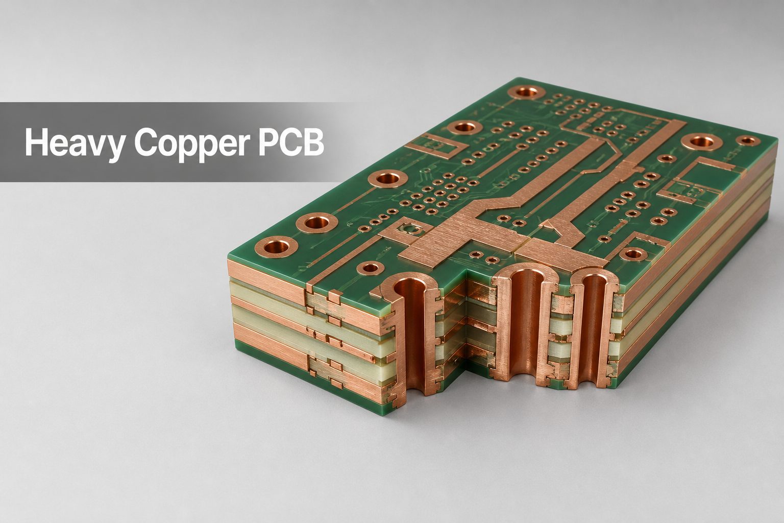
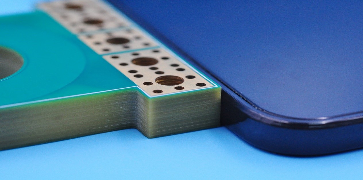
Heavy copper PCB cutaway with thick copper layers and plated through holes

What Is a Heavy Copper PCB?

A heavy copper PCB is generally understood in the PCB industry as a rigid board with copper conductors of about 3 oz/ft² or more on one or more layers. The term is not a single IPC product class, so the fabrication drawing should state the finished copper thickness required on every layer instead of relying on the words “heavy copper” alone.

Higher pcb copper weight increases the conductor cross-section available for current and heat spreading, but it also changes etching, plating, lamination, drilling, solder-mask coverage, and assembly behavior. Typical applications include power distribution, motor drives, battery systems, power converters, planar magnetics, welding equipment, industrial controls, and high-current protection circuits.

What Copper Thickness Can EBest Circuit Support?

Our current FR-4 process matrix separates routine production from special-process review. Standard designs cover inner-layer copper from 0.5 to 5 oz and outer-layer copper from 1 to 5 oz. Copper from 5 to 20 oz is listed as a special process for both inner and outer layers.

Layer position Standard process Special process Quotation status
FR-4 inner layer 0.5–5 oz 5–20 oz Confirm finished copper by layer
FR-4 outer layer 1–5 oz 5–20 oz Confirm base foil plus plating
20–200 oz extreme copper Not a standard matrix range Project-specific engineering review Stackup, size, geometry and quantity required

Our public product page describes extreme copper projects up to 200 oz. That figure should be treated as an engineering-review target, not a blanket promise that can be combined with every layer count, hole size, board dimension, material, or tolerance. A 100 oz+ request requires a dedicated feasibility review before the layout is frozen.

Which Heavy Copper PCB Stackups Are Typical?

Typical stackups keep copper mass as balanced as the electrical design allows. The exact core and prepreg construction is selected after we review copper coverage, finished board thickness, current paths, isolation requirements, hole structures, and assembly constraints.

Configuration Typical use Main DFM focus
Two-layer heavy copper Simple high-current distribution and power conversion Symmetric copper, isolation spacing and solderability
Four-layer balanced power board Separate power, ground and control functions Mirror copper weight and coverage around the centerline
Mixed-copper multilayer Heavy power layers with lighter signal layers Resin fill, lamination pressure, thickness control and registration
Extreme-copper custom construction Very high-current terminals, switches or power modules Fabrication route must be agreed before detailed layout

For stable heavy copper PCB design, avoid placing most of the copper mass on only one side of the stack. Large differences in copper coverage can increase resin-flow difficulty, thickness variation, bow, and twist. We may request copper balancing or thieving changes that do not alter the electrical function.
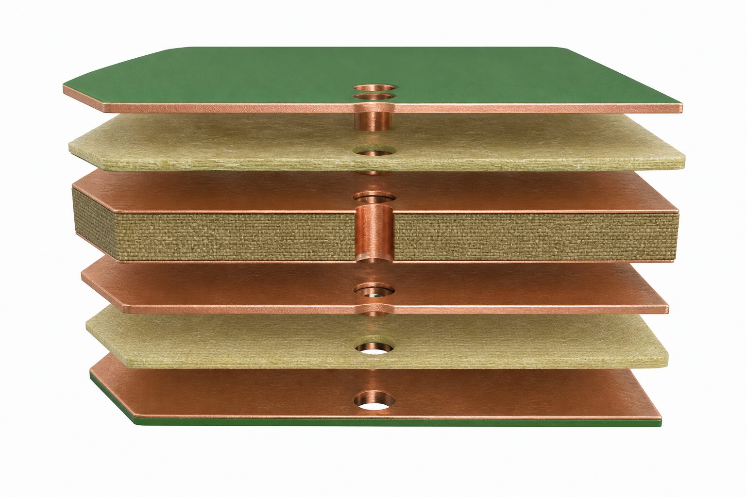
Exploded balanced multilayer heavy copper PCB stackup

Which Materials and Prepreg Systems Are Used?

FR-4 is the usual starting material, but the resin system must match the copper volume, thermal exposure, electrical requirements, and final board thickness. Our current material matrix includes low-, mid-, and high-Tg FR-4 options, with high-Tg material required for standard constructions of eight layers or more.

  • Standard FR-4 prepregs: 1080, 2116 and 7628.
  • High-Tg FR-4 examples: KB6167, ITEQ IT180, SY-S1170 and S1000-2.
  • Special material options: selected Isola, Nelco, Rogers, Taconic, PTFE and halogen-free systems, subject to stackup and procurement review.
  • Core selection: based on dielectric thickness, copper weight, required finished thickness and lamination filling demand.

Prepreg style alone does not guarantee a void-free heavy-copper build. Copper topography, remaining resin volume, pressure distribution, panel size, and copper coverage all affect fill. For deep conductor steps or 100 oz+ structures, we first review whether a conventional multilayer route is appropriate or whether a different conductor architecture is required.

Which Surface Finishes Are Available?

Available FR-4 surface finishes include OSP, HASL, ENIG, immersion silver, immersion tin, ENEPIG, hard gold fingers, and selected combined finishes. The correct option depends on pad flatness, shelf life, soldering process, contact wear, wire bonding requirements, and exposed-copper areas.

Surface finish Common selection reason Heavy-copper review point
OSP Simple solderable copper protection Handling, multiple heat cycles and exposed-copper plan
HASL / lead-free HASL Established solderable finish Surface planarity and large thermal mass
ENIG Flat pads and broad assembly compatibility Nickel/gold coverage around high copper steps
Immersion silver or tin Flat soldering surface Storage, handling and process compatibility
ENEPIG Soldering and selected wire-bonding applications Confirm bonding method and finish specification
Hard gold fingers Wear-resistant edge contacts Gold thickness, bevel and selective plating area

The finished board thickness range also varies with the selected finish. If your drawing combines thick copper with selective gold, exposed bus areas, press-fit holes, or large solder terminals, identify those regions clearly in the fabrication notes.

What Design Rules and Manufacturing Tolerances Apply?

Design rules become wider as copper thickness increases because the etching and plating window changes. Do not apply a 1 oz line/space rule to a 6, 10, or 20 oz layer. The values below are from our current FR-4 capability matrix and must still be checked against the full stackup.

Finished copper Inner standard line/space Inner special line/space Outer standard line/space Outer special line/space
2 oz 6/6 mil 5/5 mil 8/8 mil 6/6 mil
3 oz 10/12 mil 8/8 mil 12/12 mil 9/9 mil
4 oz 12/16 mil 10/10 mil 16/16 mil 12/12 mil
5 oz 16/20 mil 10/14 mil 20/20 mil 15/15 mil
6 oz 22/26 mil 14/16 mil 26/26 mil 20/20 mil
10 oz 36/40 mil 28/34 mil 40/40 mil 32/32 mil
20 oz 74/90 mil 60/80 mil 90/90 mil 70/70 mil

General FR-4 drilling tolerances in the same matrix are ±3 mil for plated-hole diameter and ±2 mil for non-plated-hole diameter under the standard process, with tighter special-process values of ±2 mil and ±1 mil respectively. Outline tolerance is typically ±5 mil. These values are not automatically combinable with maximum copper, maximum thickness, minimum holes, maximum aspect ratio, and maximum board size in one design.

Use our heavy copper PCB design guide as an early reference, then send the actual files for DFM. For current-carrying calculations, IPC-2152 relates conductor size, current and acceptable temperature rise; it does not replace thermal simulation, terminal analysis, or prototype validation for the finished assembly.

Which Via Technologies Are Available?

Through holes, mechanical blind/buried holes, and laser blind/buried vias are listed in our FR-4 capability matrix. The generic matrix shows 0.10 mm laser blind/buried vias, 0.20 mm standard mechanical blind/buried holes, and 0.15 mm special mechanical blind/buried holes.

  • Plated through holes: standard maximum aspect ratio 8:1; special process up to 10:1.
  • Mechanical blind/buried holes: 0.20 mm standard and 0.15 mm special-process minimums.
  • Laser blind/buried vias: 0.10 mm listed capability for suitable HDI constructions.
  • High-current transitions: multiple parallel vias, larger finished holes, thicker barrel copper, or direct copper structures may be considered after current and thermal review.

These minimums describe the broader FR-4 process range, not a guarantee that microvias can be combined with 20 oz or 100 oz copper. On heavy power layers, larger via structures and generous annular rings are usually more manufacturable. We confirm drill diameter, pad size, finished barrel copper, aspect ratio, and connection pattern together.
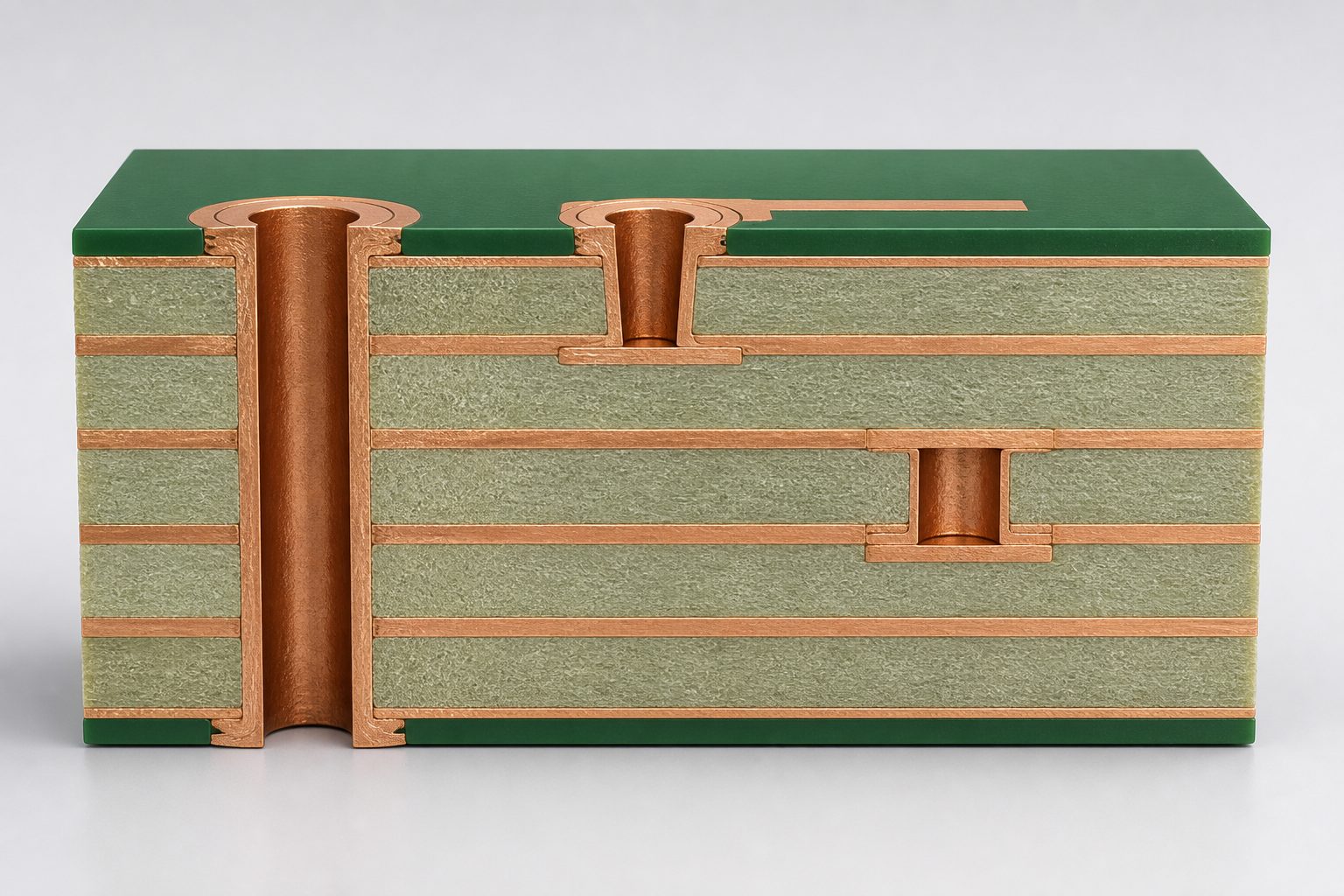
Cutaway showing through, blind and buried vias in a multilayer heavy copper PCB

Which Standards and Certifications Apply?

The applicable document set depends on the product class, end market, customer drawing, and purchase specification. A heavy copper board should not be described as “IPC compliant” without naming the exact document, revision, class, and acceptance requirements.

  • IPC-2152: guidance for determining current-carrying capacity from conductor size and acceptable temperature rise.
  • IPC-2221 and IPC-2222: generic and rigid-board design requirements.
  • IPC-6012F: qualification and performance requirements for rigid printed boards.
  • IPC-A-600: acceptability criteria for printed boards when called out with the applicable performance specification.

EBest Circuit company materials list ISO 9001:2015, ISO 13485:2016, IATF 16949, AS9100D, UL, RoHS and REACH documentation. Certification scope is not identical for every product, manufacturing site, or end use. State your industry and required certificate package in the RFQ so we can confirm the applicable manufacturing route and provide the relevant evidence.

What Determines Typical Lead Time?

Heavy copper lead time is quoted after DFM because the work does not follow one standard prototype schedule. The public EBest Circuit lead-time table directs special boards to contact us for project-specific timing, and that is the correct approach for heavy and extreme copper.

  • Finished copper weight on every inner and outer layer.
  • Layer count, board thickness, panel size and copper balance.
  • Laminate and prepreg availability, including special or halogen-free systems.
  • Mechanical, blind, buried or laser-via requirements.
  • Surface finish, selective plating and solder-mask build.
  • Prototype quantity, production quantity and test-coupon requirements.
  • DFM clarification cycles and customer approval time.

To shorten the schedule, submit a complete, internally consistent package and approve the proposed stackup before detailed routing is locked. You can review our general PCB lead-time framework, but the written quotation and order acknowledgement govern the actual heavy-copper delivery date.

How Should Engineers Design 100 oz+ PCBs?

A 100 oz+ board must be treated as an extreme copper PCB project, not as a 10 oz layout with every dimension multiplied. One ounce of copper per square foot is approximately 35 µm, so 100 oz represents roughly 3.5 mm of copper before considering dielectric layers, plating, surface finish, and fabrication tolerances.

  1. Define the electrical target. Provide continuous and peak current, duty cycle, allowed voltage drop, ambient conditions, cooling method and maximum temperature rise.
  2. Specify finished copper by layer. State which layers require 100 oz+ and whether the target includes plated build-up. Do not use one global copper note for a mixed construction.
  3. Separate power and signal needs. Keep fine-pitch control circuitry away from the extreme-copper geometry or place it on a separate assembly when practical.
  4. Use broad, simple conductors. Avoid fine neck-downs, dense spacing, small thermal spokes and abrupt current bottlenecks. Exact minimum geometry must come from project DFM.
  5. Minimize layer transitions. Where current must change layers, define the total current path through terminals, copper features and via structures rather than counting vias alone.
  6. Balance the construction. Keep copper mass and coverage as symmetric as possible to reduce lamination and flatness risk.
  7. Reserve mechanical space. Expect larger pads, holes, clearances, edge distances and finished board thickness than a normal PCB.
  8. Freeze the layout after fabricator DFM. We must agree on the manufacturing route, stackup, conductor geometry, tolerances, coupon plan and inspection criteria before release.

These are high current PCB design guidelines, not a released 100 oz design-rule table. EBest Circuit’s controlled FR-4 matrix currently provides numeric line/space rules through 20 oz. Any 100 oz+ geometry remains subject to engineering feasibility, material sourcing, panel constraints, and a written project-specific rule set.

What Should You Send for DFM Review and Quotation?

A complete package lets us distinguish a feasible heavy-copper build from a requirement that needs structural changes. Send the electrical requirements together with the fabrication data, not just Gerber files and a single copper number.

  • Gerber or ODB++ data, NC drill files, drill table and board outline.
  • Layer stackup with finished copper weight for every layer.
  • Finished board thickness, tolerance, dimensions and quantity.
  • Material family, Tg, CTI, flammability and halogen-free requirements where applicable.
  • Surface finish, selective plating, exposed copper and edge-contact requirements.
  • Continuous/peak current, temperature-rise limit, duty cycle and cooling conditions.
  • Required IPC document, class, test coupons, microsections, electrical test and certificate package.
  • Prototype target date and production forecast.

Our general PCB capability page provides broader reference data. For a binding decision, the reviewed stackup, DFM response and quotation take priority over standalone website maxima.
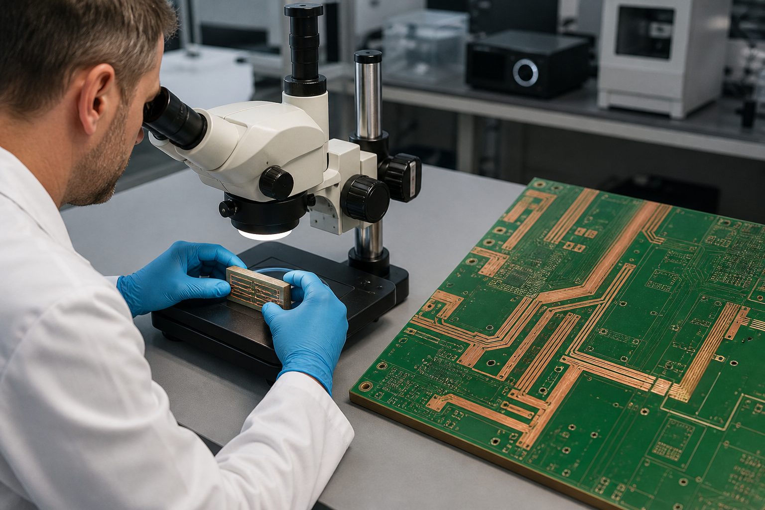
Heavy copper PCB and polished cross-section coupon under microscope inspection

FAQ About Heavy Copper PCB

Is 3 oz copper considered heavy copper?

Many PCB manufacturers use 3 oz/ft² as the practical starting point for heavy copper, although there is no single IPC definition that makes the label sufficient for fabrication. Always state the finished copper thickness required on each layer.

Can inner and outer layers use different copper weights?

Yes. Mixed-copper stackups can place heavier copper on power layers and lighter copper on signal layers. The combination must be reviewed for resin fill, copper balance, finished thickness, registration and the line/space required on each layer.

Can heavy copper PCBs use blind or buried vias?

They can in suitable constructions, but the smallest generic FR-4 via capability cannot automatically be combined with the highest copper weight. We review hole type, connection layers, annular ring, dielectric thickness and copper build together.

Does thicker copper always allow more current?

Thicker copper increases conductor cross-section, but current capacity also depends on trace width, temperature-rise limit, adjacent copper, board material, airflow, enclosure, duty cycle, terminals and layer position. Use IPC-2152 as a design reference and validate the complete assembly.

Which finish is best for a heavy copper power board?

There is no universal finish. ENIG is useful where pad flatness matters, HASL is an established solderable option, OSP is simple, and ENEPIG may support selected bonding needs. The assembly process, storage plan, contact wear and selective-plating requirements decide the finish.

Can EBest Circuit make a 100 oz PCB?

We evaluate 100 oz+ requests as extreme-copper projects. Our controlled FR-4 matrix provides standard and special rules through 20 oz, while higher public maxima require project-specific confirmation. Send the stackup, geometry, current target, board size and quantity for a written feasibility decision.

How Can EBest Circuit Support Your Heavy Copper PCB Project?

At EBest Circuit, we support heavy copper PCB stackup review, material selection, DFM, prototype fabrication, production planning, electrical testing and cross-section inspection. We will identify which requirements fit the standard process, which require a special route, and which need redesign before they become cost or reliability problems.

Send your files and operating requirements through our PCB quotation and engineering contact page. For 20 oz, 100 oz+ or mixed-copper multilayer designs, request the project-specific stackup and design rules before final layout release.

You may also like

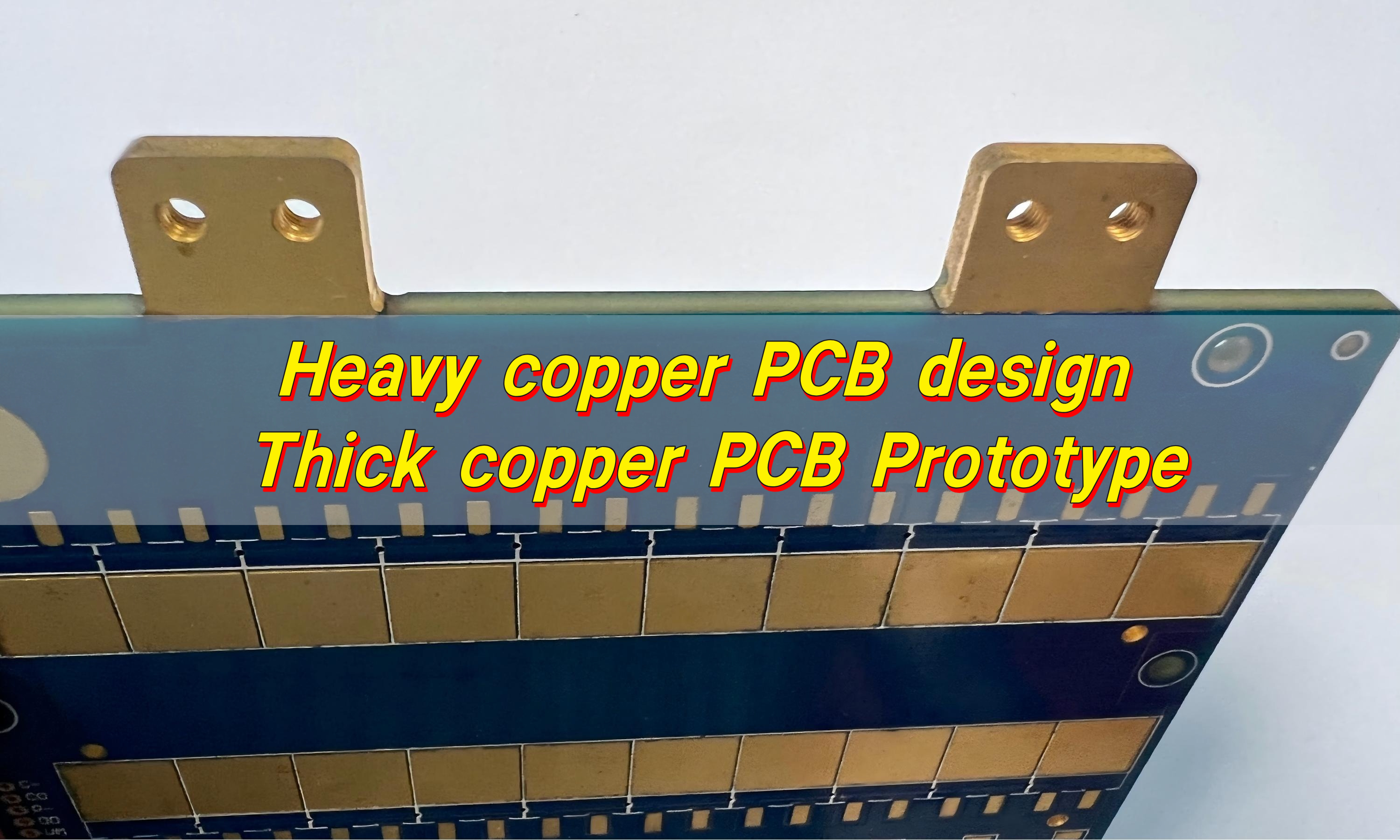
Heavy copper PCB design & Thick copper PCB Prototype​
Friday, September 5th, 2025

Heavy copper PCB design refers to creating printed circuit boards with much thicker copper layers than standard boards. While a typical PCB uses 1 oz copper (about 35µm), heavy copper PCBs range from 2 oz to 20 oz per square foot, sometimes even higher for extreme power needs.

Thick copper layers improve current handling, enhance mechanical strength, and allow for compact, high-power layouts without compromising reliability.

Heavy copper PCB design & Thick copper PCB Prototype​

What is heavy copper PCB?

Heavy copper PCB uses copper conductors that are much thicker than standard PCBs. While standard boards use 1 oz copper (about 35µm), heavy copper boards range from 2 oz to 20 oz per square foot. Some extreme designs even go beyond that, which we call extreme copper PCB.

So, why so thick? Because thicker copper carries more current without overheating. It also improves mechanical strength, making the board more robust for harsh environments.

In short, heavy copper PCBs are not ordinary. They are designed for power electronics, automotive, defense, and industrial equipment that demand strength and stability.

Why use thick copper PCB?

Power systems produce heat. A lot of it. If your PCB cannot handle high current, failure is just a matter of time. That’s why thick copper PCBs are vital.

Here’s why industries love them:

  • Superior current capacity: Thick copper allows higher amperage without damaging traces.
  • Better heat dissipation: No more overheating issues in power circuits.
  • Strong mechanical bonding: Ideal for connectors, heavy components, and thermal sinks.
  • Design flexibility: Perfect for high-density interconnects and power distribution layers.
Heavy copper PCB design & Thick copper PCB Prototype​

When reliability is non-negotiable, heavy copper PCB design is the answer.

How thick is copper in a heavy copper PCB?

Thickness matters. A standard PCB has 1 oz copper (35µm). For heavy copper PCBs, the thickness ranges from:

  • 2 oz (70µm): Entry-level heavy copper
  • 3 oz to 6 oz (105µm to 210µm): Common for power electronics
  • 8 oz to 20 oz (280µm to 700µm): Extreme copper PCB for very high power

The choice depends on current requirements, thermal performance, and mechanical strength. If your design demands high current flow, you need more copper.

What are the common problems in heavy copper PCB design?

Designing a heavy copper PCB is not as simple as adding more copper. It brings challenges:

  • Etching Issues: Thick copper needs deeper etching, which requires advanced technology.
  • Uneven Trace Widths: Incorrect design may lead to imbalance.
  • Plating Difficulties: High copper density affects via plating and reliability.
  • High Cost: More copper equals higher material and manufacturing cost.

With a professional heavy copper PCB manufacturer like BEST Technology, these challenges are easily solved. Our team uses controlled etching and advanced plating to ensure accuracy and quality.

How much does heavy copper price affect cost?

The price of heavy copper PCBs depends on:

  • Copper weight (2 oz, 4 oz, 6 oz, etc.)
  • Board size and layer count
  • Design complexity
  • Quantity
Heavy copper PCB design & Thick copper PCB Prototype​

Copper is not cheap. A 6 oz PCB will cost more than a 2 oz PCB due to more copper and processing time. If you want exact pricing, contact us at sales@bestpcbs.com. Our experts will provide a detailed quotation and free consultation.

What are the benefits of thick copper PCB?

The benefits are undeniable:

  • High current carrying capacity: Perfect for power supplies and converters.
  • Excellent heat dissipation: Reduces thermal stress on components.
  • Stronger mechanical strength: Holds heavy connectors and components.
  • Compact design: Combine power and control circuits on one board.
  • Reliable in harsh environments: Ideal for automotive and military.

Simply put, heavy copper PCBs improve performance and extend the lifespan of your devices.

Why choose BEST Technology for heavy copper PCBs?

Because we deliver:

  • Copper thickness from 2 oz to 20 oz with precision.
  • Advanced etching technology for accurate trace widths.
  • Superior plating process for reliable via connections.
  • ISO9001:2015 certified manufacturing.
  • Short lead time: Fast delivery for your projects.

Our heavy copper boards are used in power converters, inverters, automotive systems, and defense equipment worldwide.

BEST Technology Heavy Copper PCB Capabilities

Specification Category Details
Base material FR4/Aluminum
Copper thickness 4OZ ~ 10OZ
Extreme Heavy Copper 20OZ ~ 200OZ
Outline Routing, Punching, V-Cut
Soldermask White/Black/Blue/Green/Red Oil
Surface finishing Immersion Gold, HASL, OSP
Max Panel size 580 × 480 mm (22.8″ × 18.9″)

What are the applications of heavy copper PCBs?

These boards are everywhere in high-power industries:

  • Power Supply Modules
  • Automotive Electronics
  • Military and Defense Systems
  • Renewable Energy Systems (Solar, Wind)
  • Industrial Control Equipment
  • Telecom Base Stations

If your design needs high current handling and thermal stability, heavy copper is the only way.

Heavy copper PCB manufacturers – BEST Technology

Not all manufacturers can handle thick copper PCBs. It requires specialized equipment, strict process control, and experience. That’s where BEST Technology stands out.

We’ve been manufacturing heavy copper PCBs since 2006. Our factory is equipped for multi-layer heavy copper boards, extreme copper designs, and custom prototypes. We handle everything from design support to mass production.

Heavy copper PCB design & Thick copper PCB Prototype​

When you choose us, you get:

  • Expert engineering support
  • Competitive pricing
  • On-time delivery
  • High-quality boards for critical applications

Conclusion:

Heavy copper PCB design is a requirement for high-power electronics. They offer superior current capacity, heat dissipation, and mechanical strength.

If you’re looking for professional heavy copper PCB manufacturers, BEST Technology is your trusted partner. Contact us at sales@bestpcbs.com for a quote, technical support, or free consultation.

You may also like

Extreme Copper PCB Supplier, One Stop Solution
Tuesday, July 29th, 2025

Looking for extreme copper PCB solutions? This guide covers specs, benefits, applications and design guidelines for extreme copper PCB.

Are you troubled with these problems?

  • Frequent PCB failures in high-current scenarios?
  • Is the cost of cooling solutions out of control?
  • Half the lifespan in harsh environments?

EBest Circuit (Best Technology) can provide solutions:

  • 4-20oz stepped copper layer: Minimum trace width of 0.8mm achieves 600A continuous current.
  • 3D heat dissipation topology: 0.5mm microvia clusters + copper pillar soldering, reducing thermal resistance by 40%.
  • Environmentally adaptable coating: Passed 72-hour dual 85 test, IP67 protection level.

Welcome to contact us if you have any request for heavy copper PCB: sales@bestpcbs.com.

What Is Extreme Copper PCB?

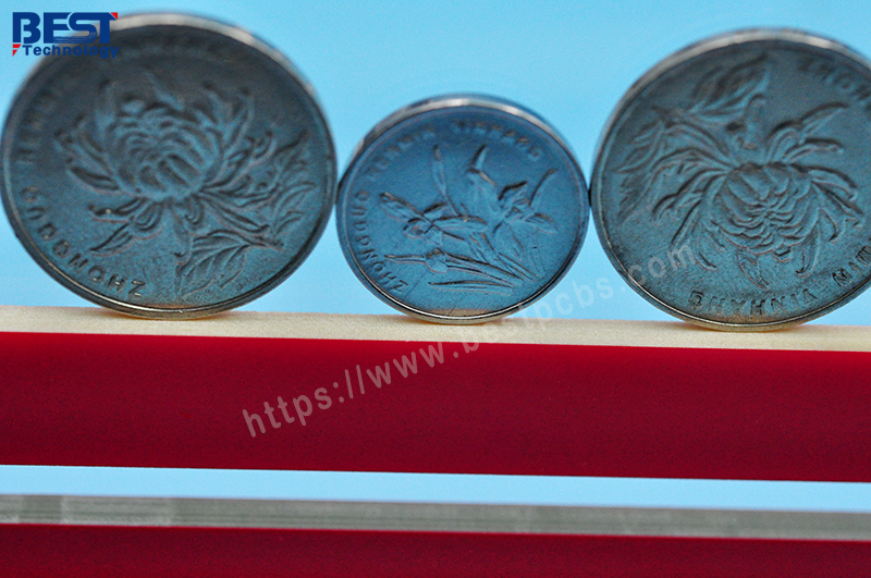
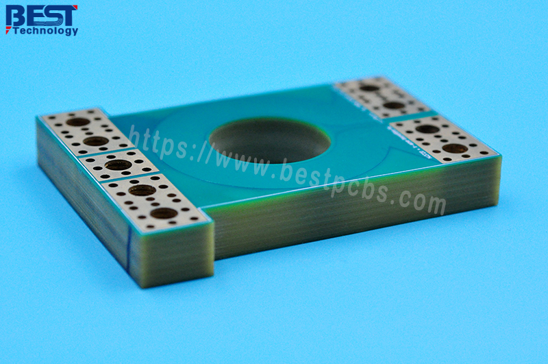
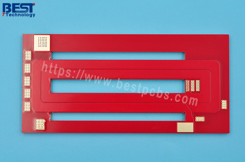
An extreme copper PCB is a special type of printed circuit board that uses extra-thick copper layers, typically starting from 5 oz/ft² (about 175 microns) and going up to 20 oz/ft² or even higher. These thick copper layers are far greater than the standard 1 oz or 2 oz copper found in most PCBs. The goal of using extreme copper is to handle very high current, manage intense heat, and ensure mechanical durability in harsh environments.

Unlike standard copper PCB boards, extreme copper PCBs can safely conduct large currents without overheating, thanks to the increased cross-sectional area of the copper traces. In addition, the thick copper enhances the board’s thermal conductivity and mechanical strength, making it highly reliable for long-term use in demanding applications.

What Is Extreme Copper PCB?

Extreme Copper PCB Specification

ParameterSpecification
Copper Thickness5 oz/ft² to 20 oz/ft² (175 µm to 700 µm)
Base MaterialHigh TG FR4, Polyimide, Metal Core (Aluminum or Copper), Ceramic
Board Thickness1.6 mm to 6.0 mm (customizable)
Minimum Trace Width/Spacing0.5 mm / 0.5 mm (may vary based on copper thickness and design)
Maximum Current CapacityUp to 100 Amps or more, depending on trace width and copper weight
Thermal ConductivityHigh, due to thick copper and thermal vias (1.0–3.0 W/m·K for standard FR4)
Surface Finish OptionsENIG (Immersion Gold), HASL, OSP, Immersion Silver, Hard Gold
Drill Hole SizeMinimum 0.3 mm (12 mil), larger holes recommended for thick boards
Layer Count1 to 6 layers (commonly 1–2 layers for extreme copper)
Impedance ControlPossible with careful design; may be challenging due to thick copper
Solder MaskHigh-temperature resistant (e.g., green, black, white, custom colors)
Plating TypeHeavy copper plating for traces, pads, and through-holes
Thermal Via SupportYes – often required for heat dissipation in multilayer or dense designs
Standards ComplianceIPC-6012 Class 2/3, RoHS, UL94-V0 flame retardant rating

What Are Benefits of Extreme Copper PCB?

Breaking Current-Carrying Limits

  • A single 4oz (140μm) copper layer can carry 50A, four times the current of a conventional 1oz PCB.
  • Multi-layer stacking solutions (such as a 2oz + 4oz combination) support high-current transmission exceeding 1000A.

Reduced System Temperature Rise Risk

  • Tests show that under the same load, the temperature rise of a 4oz copper plate is 40% lower than that of a 1oz copper plate.
  • Reduced heat sink size enables device miniaturization.

Extended Product Lifecycle

  • The fatigue strength of the copper layer is increased by 60%, preventing circuit cracking caused by high-frequency vibration.
  • Salt spray testing shows corrosion resistance is three times that of conventional PCBs.

Simplified System Design Complexity

  • Multiple low-voltage circuit boards can be combined into a single board, reducing connectors and wiring harnesses.
  • Supports integrated power/signal design, reducing EMI interference.

Lifecycle Cost Advantages

  • Although the initial cost increases by 20%, the failure rate decreases by 70%.
  • A five-year TCO (Total Cost of Ownership) calculation shows a 35% reduction in maintenance costs.
What Are Benefits of Extreme Copper PCB?

What Are Applications of Extreme Copper PCB?

Applications of Extreme Copper PCB

  • Power Electronics– Used in power supplies, converters, and inverters to handle high current and heat.
  • Automotive Systems– Ideal for electric vehicle chargers, battery management systems, and motor controllers.
  • Industrial Equipment– Applied in welding machines, heavy machinery, and high-power control systems.
  • Military and Aerospace– Used in radar systems, communication devices, and rugged electronics for harsh conditions.
  • Renewable Energy– Found in solar inverters and wind power controllers that require high reliability and heat resistance.
  • Railway and Transportation– Used in power control units and signaling systems that demand strong and durable PCBs.
  • Medical Devices– Suitable for high-power medical equipment requiring stable and safe operation.

Extreme Heavy Copper PCB Design Guide

1. Material Selection

  • Base Material: Use high-Tg (≥180°C) FR4 or ceramic-filled PTFE for thermal stability.
  • Copper Foil: Specify 6-10 oz (210-350µm) rolled annealed copper for flexibility and adhesion.
  • Metal Core: Integrate aluminum/copper substrates (e.g., 2mm thickness) for direct heat dissipation.

2. Layer Stackup Strategy

  • Outer Layers: 6-10 oz copper for power/ground paths.
  • Inner Layers: 2-4 oz copper for signals; add isolated power planes for high-current rails.
  • Thermal Vias: Place 0.8-1.2mm diameter vias (≥3 oz plating) under hot components to connect outer/inner layers.

3. Trace Design Rules

  • Calculate width using IPC-2221 (e.g., 10 oz copper = ~150A for 20mm trace at 10°C rise).
  • Use 45° bends; avoid right angles to reduce impedance spikes.
  • Thicken traces near connectors (e.g., 2x nominal width) to handle surge currents.

4. Thermal Management

  • Fill unused areas with copper pours (≥70% coverage) tied to ground/power planes.
  • Use embedded heat sinks (e.g., copper coins) under MOSFETs/IGBTs.
  • For metal-core boards, bond components directly to the substrate with thermal epoxy.

5. Power Distribution

  • Split power planes by voltage (e.g., 48V, 12V) to minimize noise.
  • Place decoupling capacitors (e.g., 10µF ceramic) within 2mm of IC power pins.
  • Widen battery-to-load paths (e.g., 50mm+ traces) to minimize IR drop.

6. Signal Integrity

  • Keep high-speed traces (>100MHz) away from power zones (≥5mm gap).
  • Adjust trace spacing to maintain 75-100Ω impedance despite thick copper.
  • Use guard traces (grounded copper) around sensitive signals.

7. Manufacturing Compliance

  • Specify “extreme heavy copper” and “metal-core” in design notes.
  • Confirm minimum trace/space (≥10mil) and via drill sizes (≥0.5mm).
  • Request differential etching and X-ray inspection for via plating quality.

8. Assembly Considerations

  • Use high-temperature solder (e.g., SAC305) rated for 260°C reflow.
  • Add soldermask dams between thick traces to prevent solder wicking.
  • Test prototypes with 2x nominal current to validate thermal performance.

9. Validation & Testing

  • Perform thermal imaging under max load to identify overheating zones.
  • Use a microsection analysis to verify copper thickness and via plating integrity.
  • Conduct HALT (Highly Accelerated Life Test) for thermal cycling (-40°C to +125°C).
Extreme Heavy Copper PCB Design Guide

Why Choose EBest Circuit (Best Technology) as Extreme Copper PCB Supplier?

Reasons why choose us as extreme copper PCB supplier:

  • Certified Compliance (ISO 9001, UL, RoHS) – Mitigates regulatory risks and ensures products meet global standards for safety and environmental compliance.
  • 19 Years of Heavy Copper PCB Manufacturing Experience – Quickly and flexibly handle the production of thick copper plates, speeding up production cycles。
  • 24-Hour Rapid Prototyping Delivery – Accelerates product development cycles, enabling faster time-to-market and competitive edge in high-demand industries.
  • Stringent Quality Control with 100% Inspection – Eliminates hidden defects, reduces rework costs, and ensures reliability in high-current/thermal applications.
  • Transparent Pricing with No Hidden Fees – Predictable budgeting and cost savings through upfront pricing models tailored to thick copper PCB specifications.
  • Free DFM (Design for Manufacturability) Analysis – Optimizes PCB layouts to reduce material waste, lower production costs, and avoid late-stage design revisions.
  • One-Stop Solution from Design to Delivery – Streamlines project management by consolidating prototyping, fabrication, and assembly under one roof.
Why Choose EBest Circuit (Best Technology) as Extreme Copper PCB Supplier?

Our Heavy Copper PCB Capabilities

Base materialFR4/Aluminum
Copper thickness:4 OZ~10 OZ
Extreme Heavy Copper:20~200 OZ
Outline:Routing, punching, V-Cut
Soldermask:White/Black/Blue/Green/Red Oil
Surface finishing:Immersion Gold, HASL, OSP
Max Panel size:580*480mm(22.8″*18.9″)

How to Get A Quote For Extreme Copper PCB Project?

Basic structural parameters

  • Number of layers required (single-sided/double-sided/4-20 layers)
  • Finished product dimensions (length x width ± tolerance) and panelization plan
  • Panel type (FR4 Tg 170°/aluminum substrate/ceramic substrate
  • Target board thickness (0.8-6.0mm range)

Copper foil process specifications

  • Copper thickness distribution (e.g., outer layer 4oz/inner layer 2oz)
  • Special requirements (locally thickened copper block/embedded copper heat sink)
  • Minimum trace width/spacing (e.g., 6oz copper thickness requires ≥5.0mil)

Electrical performance requirements

  • Current carrying capacity (e.g., continuous current ≥200A @ 25°C)
  • Impedance control requirements (differential pair impedance value and tolerance)
  • Insulation withstand voltage rating (power frequency/DC withstand voltage)

Surface finish options

  • Choose one of: ENIG/immersion tin/OSP
  • Solder mask color (default green, other colors +20% fee)
  • Silkscreen requirements (character height ≥0.8mm)

Special process instructions

  • Thick copper etching compensation solution (design documents required)
  • Thermal via design (aperture diameter/pitch/filler material)
  • Acceptance criteria (IPC-6012D) Class 2/3)

Required Documents

  • Gerber (RS-274X format) + drill file.
  • Stackup diagram (with copper thickness distribution).
  • Impedance calculation table (if high-speed signals are involved).

Why choose EBest Circuit (Best Technology)?

  • 19 Years of Thick Copper Expertise: Delivered over 50 million 4oz+ PCBs since 2006, a strategic supplier to Tesla and Huawei.
  • Pricing Transparency: Vertically integrated supply chain, prices 30-40% lower than those of European and American manufacturers for comparable processes.
  • Extreme Response: 24-hour emergency proofing, 72-hour first-part delivery (industry average: 7 days).
  • Full Inspection Commitment: 100% AOI + Flying Probe Testing, CPK ≥ 1.67, Failure Rate < 50 PPM.
  • One-Stop Service: From design review to conformal coating to assembly and testing, complete management.

Welcome to contact us if you have any request for copper PCB: sales@bestpcbs.com.

You may also like

Heavy Copper PCB Manufacturers, Extreme Copper PCB
Sunday, March 30th, 2025

Heavy copper PCB manufacturers play a crucial role in creating circuit boards that handle high currents, distribute heat efficiently, and meet the needs of demanding industries. Whether you’re looking for extreme copper PCBs, 20oz copper PCBs, or a custom copper core PCB, understanding the factors that affect their design, quality, and assembly process will help you choose the proper manufacturer for your needs.

Heavy copper PCB (Printed Circuit Board) is a go-to solution for high-performance applications that require durability. EBest Circuit (Best Technology) provides high-quality Heavy copper PCB in the PCB industry. We provide rapid prototypes within 24-48 hours. We have offered more than 1,200 customers in more than 60 countries & areas the fast turnaround heavy copper PCB service. We provide both normal delivery service and fast service, and urgent boards can be shipped out within 24 hours! EBest Circuit (Best Technology) is one of the professional heavy copper PCB Manufacturers, if you need heavy copper PCB design, prototype, or assembly, pls feel free to reach out to EBest Circuit (Best Technology) at sales@bestpcbs.com at any time.

Heavy Copper PCB Manufacturers, Extreme Copper PCB

What Design Factors Do Heavy Copper PCB Manufacturers Consider for Reliability?

When designing heavy copper PCBs, manufacturers have to consider a wide range of factors to ensure the board performs reliably over time. Copper thickness, trace width, and the material’s ability to handle high current loads are just a few of the key considerations.

The first important design factor is the copper trace width. For high-current applications, manufacturers use wider copper traces to handle the increased load without overheating. This is especially important in industries like automotive, telecommunications, and power electronics, where PCB durability and performance are critical.

Another crucial aspect is layer stacking. Manufacturers use multiple layers in heavy copper PCBs to ensure that the heat generated by high currents can dissipate efficiently. This helps prevent thermal buildup, which can lead to failure or damage to the PCB. The layers are carefully arranged to maximize heat dissipation and ensure optimal performance under load.

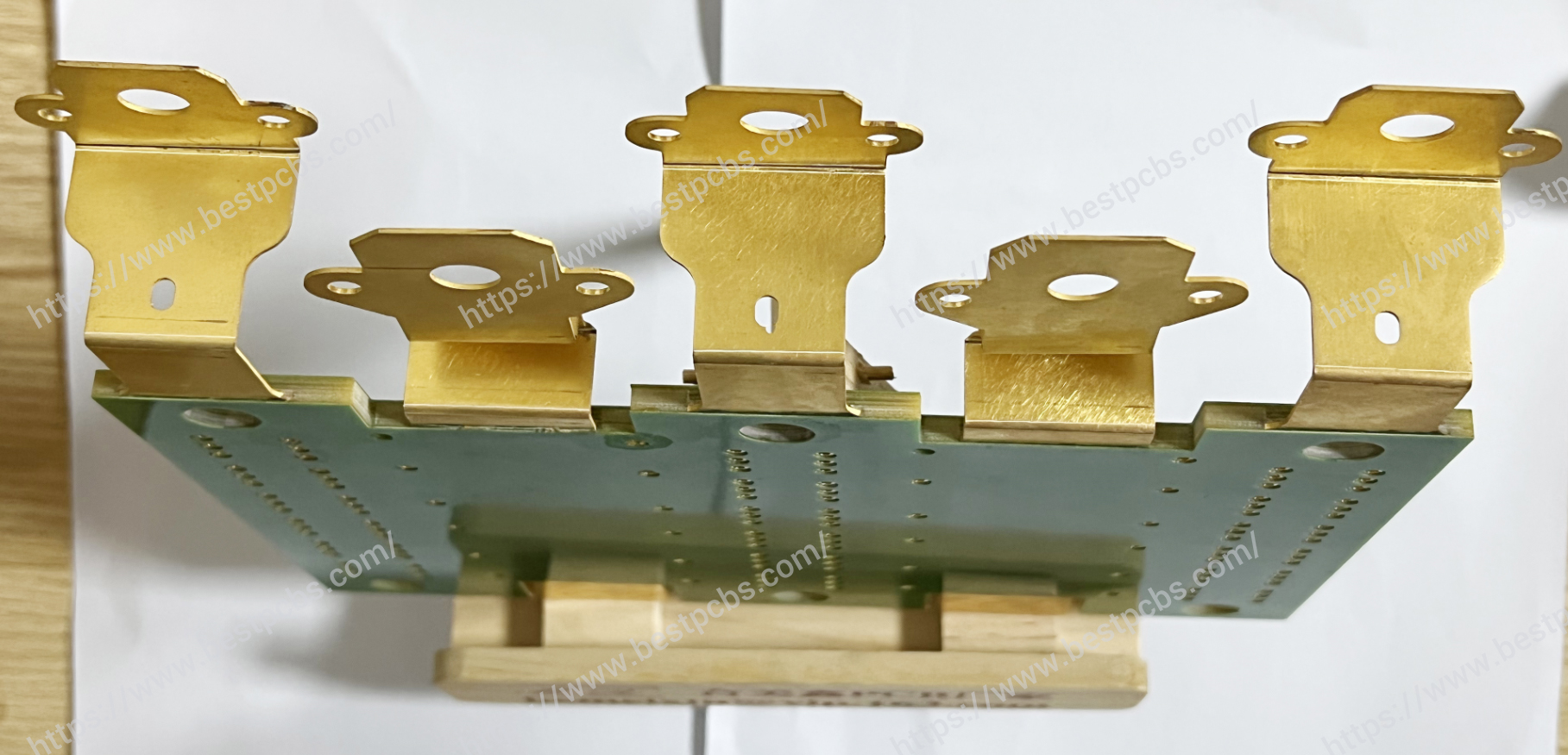
Heat dissipation techniques are also a major design factor. A properly designed heavy copper PCB uses advanced techniques, such as copper coin technology, which places thick copper elements within the PCB to efficiently absorb and dissipate heat.

Heavy Copper PCB Manufacturers

Where to Find Reliable Heavy Copper PCB Manufacturers for PCBs?

Finding the right manufacturer is key to ensuring you get a high-quality heavy copper PCB that meets your specifications. The process of identifying reliable manufacturers often starts with online research. There are numerous online directories, trade shows, and industry events where you can find reputable heavy copper PCB manufacturers.

Customer reviews and feedback play a significant role in identifying reliable manufacturers. Look for companies that have a proven track record in producing high-quality heavy copper PCBs. EBest Circuit (Best Technology), for instance, has built a strong reputation over 18 years, delivering excellent products to industries around the world.

Industry certifications also signal reliability. Established manufacturers often have certifications such as ISO 9001, UL, and IPC, which indicate their adherence to international quality standards.

Networking is another great way to find trusted manufacturers. Industry forums, LinkedIn, and professional groups offer recommendations from other businesses that have worked with these manufacturers.

Extreme Copper PCB

What Certifications Should Reliable Heavy Copper PCB Manufacturers Have?

Choosing a reliable heavy copper PCB manufacturer requires understanding the certifications they hold. Certifications are an assurance that the manufacturer follows quality control procedures and complies with industry standards.

The ISO 9001 certification is a widely recognized standard that shows a manufacturer’s commitment to quality management. It ensures that the manufacturer has consistent processes in place to deliver high-quality products.

The UL certification is another important factor, especially for PCBs that will be used in safety-critical applications. UL certification indicates that the manufacturer meets safety standards and that their products are safe for use in electrical applications.

Lastly, IPC certifications (such as IPC-A-600 and IPC-2221) demonstrate that the manufacturer follows best practices for PCB design, assembly, and inspection. These certifications ensure that the manufacturer produces PCBs that meet industry standards for performance and reliability.

What Is the Thickness of Copper in EBest Circuit (Best Technology)?

EBest Circuit (Best Technology) offers a range of copper thickness options tailored to different applications. Below is the capability of heavy copper PCB for your reference:

  • Base material: FR4/Aluminum
  • Copper thickness: 4 OZ~10 OZ
  • Extreme Heavy Copper: 20~200 OZ
  • Outline: Routing, punching, V-Cut
  • Solder mask: White/Black/Blue/Green/Red Oil
  • Surface finishing: Immersion Gold, HASL, OSP
  • Max panel size: 580*480mm(22.8″*18.9″)

EBest Circuit (Best Technology) doesn’t do “one-size-fits-all.” Our copper range fits every need. 2 oz (70 µm) is commonly used in consumer gadgets like phones, and routers. 4–10 oz heavy copper PCB is suitable for industrial applications like solar inverters.  20–200 oz extreme copper PCB is perfect for power substations and other areas that require heat dissipation and high current-carrying capacity. By customizing the copper thickness, EBest Circuit (Best Technology) ensures that each PCB meets the specific needs of its customers, whether for high-frequency applications or power electronics.

How Thick Is 2 oz of Copper for PCB?

A 2 oz copper PCB typically has a thickness of around 70 microns (2.8 mils). While this is considered a mid-range thickness, it offers significant advantages over standard copper PCBs. The thicker copper enables the PCB to handle more current and provides better thermal performance, making it ideal for applications in industrial machinery, power supplies, and automotive systems.

The added copper thickness also improves the board’s resistance to thermal stress, which is particularly important in environments where heat is generated due to high power loads.

How Do Heavy Copper PCB Manufacturers Ensure Quality and Durability?

Ensuring the quality and durability of heavy copper PCBs is a multi-step process. From the initial design phase to the final assembly, manufacturers must employ strict quality control measures.

At EBest Circuit (Best Technology), advanced technologies like automated optical inspection (AOI) and X-ray inspection are used to detect potential defects early in the production process. These tools ensure that any issues are identified and corrected before they affect the final product.

Manufacturers also use high-quality materials like copper foil and ensure that the lamination process is carried out under precise conditions to avoid defects. Each PCB undergoes thorough testing to verify its electrical properties, mechanical strength, and heat dissipation capabilities.

Heavy Copper PCB Manufacturers

How to Choose a Heavy Copper PCB Manufacturer?

Choosing the right heavy copper PCB manufacturer requires careful consideration of several factors:

  • 1. Experience: Look for manufacturers with experience in producing heavy copper PCBs, especially for the type of application you’re targeting.
  • 2. Technology: Ensure the manufacturer has the latest technology for PCB design, fabrication, and testing.
  • 3. Customer Service: A good manufacturer will offer support throughout the entire process, from design to assembly.
  • 4. Prototyping: Request prototypes to verify the manufacturer’s capabilities before committing to large-scale production.

By evaluating these factors, you can choose a manufacturer that meets your quality standards and provides a seamless experience from start to finish.

Finally, heavy copper PCB manufacturers are essential partners for businesses in need of high-performance and durable PCBs. EBest Circuit (Best Technology) stands out as a reliable provider of heavy copper PCBs, offering customized solutions and unparalleled expertise. Whether you need extreme copper PCBs or 20oz copper PCBs, choosing the proper manufacturer ensures the success and longevity of your products.

Do you need a heavy copper PCB solution? Just feel free to contact EBest Circuit (Best Technology) at sales@bestpcbs.com at any time for expert guidance, exceptional quality, and fast delivery.

You may also like