PCB manufacturing PCB manufacturing
Home > Blog

High Current PCB Design Guidelines

Heavy Copper PCB Manufacturer for High Current and Power Applications
Friday, August 28th, 2026

A heavy copper PCB manufacturer builds boards for applications that require higher current capacity, improved heat dissipation, and stronger mechanical reliability than standard copper PCB constructions. By increasing copper thickness on inner or outer layers, these PCBs can support high-power circuits used in battery systems, power converters, industrial equipment, EV charging systems, renewable energy controls, and other demanding electrical applications.

EBest Circuit provides custom heavy copper PCB manufacturing with support for thick copper layers, mixed copper stack-ups, high-current designs, and complex multilayer structures. Our engineering team reviews copper thickness, layer configuration, thermal requirements, via structures, and manufacturing feasibility before production to help customers develop reliable power PCB solutions. Send your Gerber files, stack-up requirements, or application details to sales@bestpcbs.com for engineering review and quotation.
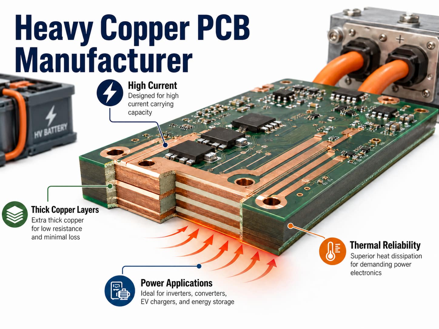
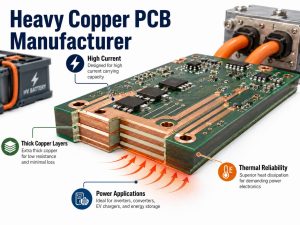
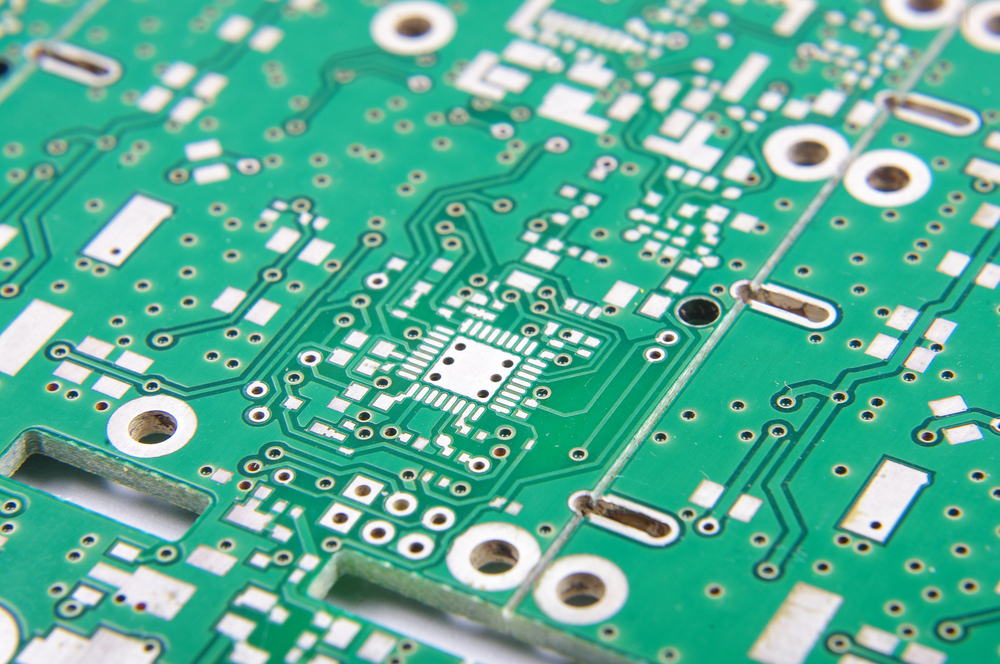
Heavy copper PCB with thick copper layers for high-current power applications

What Maximum Copper Thickness Can Be Achieved for Heavy Copper PCBs?

The maximum copper thickness of a heavy copper PCB depends on the layer position, board size, copper distribution, etching requirements, and manufacturing process capability. Unlike standard PCBs using 1 oz or 2 oz copper, heavy copper designs require specialized processing to maintain copper thickness consistency and reliable circuit formation.

EBest Circuit supports the following verified standard and special-project copper ranges. PCB copper weight must be evaluated with board size, copper distribution, spacing, dielectric fill, and process requirements.

Copper Location Typical Thickness Capability
Inner layer copper Standard 0.5–5 oz; special projects 5–20 oz
Outer layer copper Standard 1–5 oz; special projects 5–20 oz
Mixed copper designs Available after stack-up and DFM review
100 oz+ request Project-specific engineering review; not a standard capability

For 100 oz+ copper PCB designs, additional engineering evaluation is required because extremely thick copper affects:

  • Trace geometry and etching compensation
  • Copper distribution balance
  • Lamination pressure and resin filling
  • Thermal stress during manufacturing
  • Finished board weight and mechanical strength

Heavy copper capability is not only determined by copper thickness. A reliable manufacturing process must also maintain proper layer alignment, insulation spacing, and plated hole quality.

What Heavy Copper PCB Stack-Up Configurations Are Available?

Heavy copper PCBs can be manufactured with different stack-up structures depending on current requirements, thermal performance, signal requirements, and cost targets.
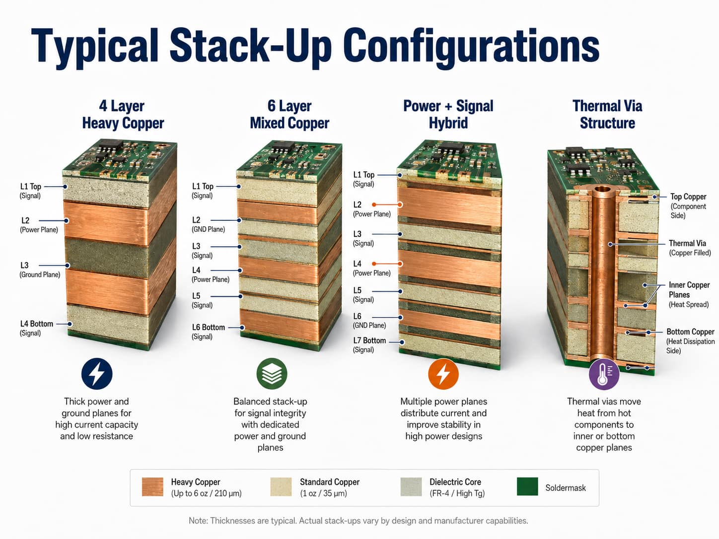
Typical four-layer, six-layer, mixed-copper, and thermal-via PCB stack-up configurations

Typical configurations include:

Stack-Up Type Typical Application
4-layer heavy copper PCB Power control boards, industrial electronics
6-layer mixed copper PCB Power and signal integration
Heavy copper outer layers with standard inner layers High current connection areas
Heavy copper power layers with thermal vias Heat-sensitive applications

A high current PCB stackup often combines heavy copper layers with standard signal layers. This approach allows engineers to increase current capacity in specific areas without unnecessarily increasing the cost and weight of the entire PCB.

A typical multilayer structure may include:

  • Thick copper power planes for current distribution
  • Standard copper signal layers for control circuits
  • Dedicated thermal layers for heat spreading
  • Controlled impedance layers when high-speed signals are required

The final stack-up should be reviewed during the engineering stage to ensure copper thickness, dielectric thickness, and manufacturing capability are properly matched.

Which Materials and Prepreg Systems Are Used for Heavy Copper PCBs?

Heavy copper PCB materials must provide sufficient mechanical strength, thermal stability, and reliable insulation performance under high current operation.
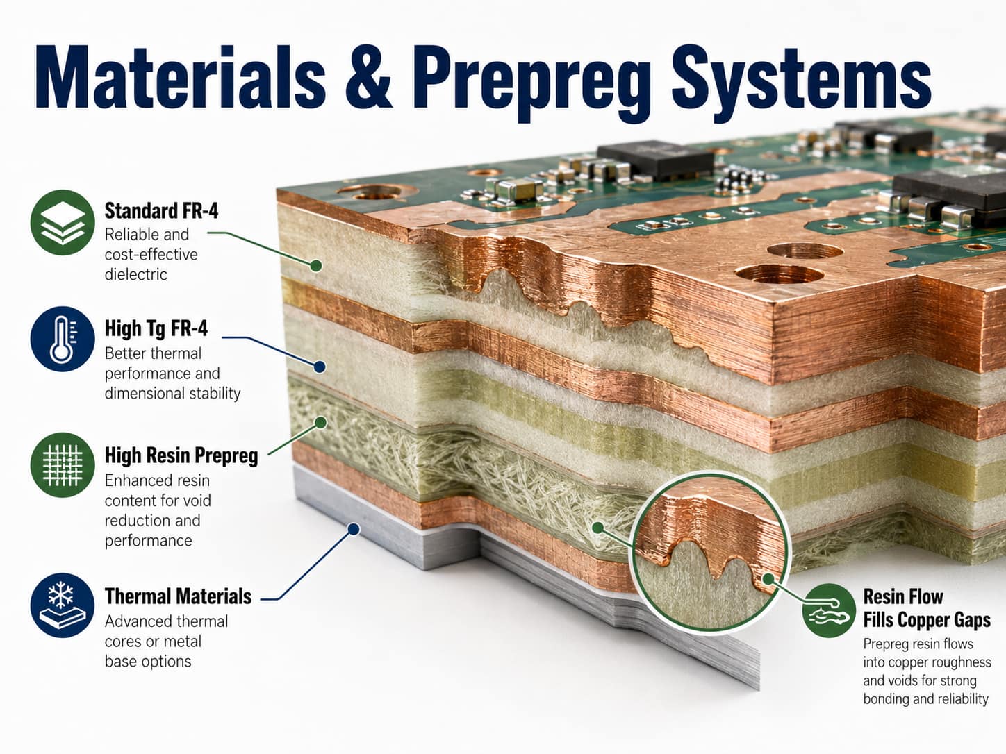
FR-4, high-Tg FR-4, high-resin prepreg, and thermal material systems for heavy copper PCBs

Common material options include:

Material System Application Advantage
Standard FR-4 General heavy copper applications
High Tg FR-4 Higher thermal reliability
Thermal management materials Improved heat dissipation
High resin content prepreg Better copper gap filling

Prepreg selection is especially important for heavy copper multilayer boards. Thick copper creates larger height differences between copper areas, requiring sufficient resin flow during lamination to prevent voids and ensure reliable insulation.

Material selection depends on:

  • Operating temperature
  • Current load
  • Thermal cycling requirements
  • Mechanical environment
  • Industry requirements

For high-power applications, engineers should consider both copper thickness and laminate performance rather than focusing only on copper weight.

What Surface Finish Options Are Available for Heavy Copper PCBs?

Surface finish selection depends on component requirements, assembly process, reliability expectations, and storage conditions.
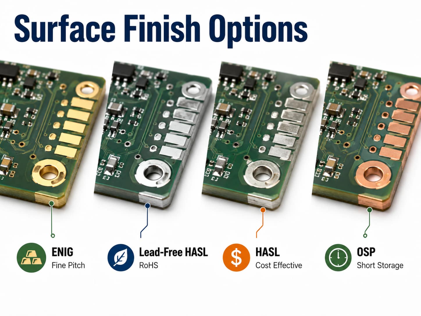
ENIG, lead-free HASL, HASL, and OSP surface finish options for heavy copper PCBs

Common surface finishes for heavy copper PCBs include:

Surface Finish Typical Application
ENIG Fine-pitch components and high reliability applications
Lead-free HASL Cost-effective industrial applications
HASL Traditional soldering applications
OSP Short-term storage and standard assembly

For high-current PCBs, surface finish selection should also consider:

  • Contact reliability
  • Solder joint performance
  • Assembly temperature profile
  • Long-term environmental exposure

The correct surface finish helps maintain reliable electrical connections throughout the product lifecycle.

What Are the Design Rules and Manufacturing Tolerances for Heavy Copper PCBs?

Heavy copper PCB design requires additional attention compared with standard PCB manufacturing because thicker copper changes trace geometry, spacing requirements, and fabrication conditions.

Important design considerations include:

Design Factor Engineering Consideration
Trace width and spacing Requires copper thickness compensation
Copper distribution Avoid excessive imbalance between layers
Clearance Must consider thicker copper profiles
Impedance control Requires stack-up-based calculation
Thermal design Optimize copper planes and heat paths

During DFM review, engineers typically evaluate:

  • Copper thickness versus minimum trace width
  • Etching capability
  • Layer-to-layer registration
  • Resin filling conditions
  • Finished board thickness

These high current PCB design guidelines should be confirmed against the proposed copper weight and stack-up during an engineering DFM review. Early communication helps avoid unnecessary redesign during manufacturing.

Which Via Technologies Are Available for Heavy Copper PCB Manufacturing?

Via structures play an important role in heavy copper PCB performance because they influence current flow, thermal transfer, and mechanical reliability.

Available via technologies include:

  • Through-hole vias
  • Plated through vias
  • Thermal via arrays
  • Large diameter vias
  • Multiple parallel vias for current distribution

For power applications, engineers often use multiple thermal vias under heat-generating components or create parallel via paths to reduce electrical resistance.

Via design should consider:

  • Current requirements
  • Component heat generation
  • Copper thickness
  • Assembly conditions

A proper via structure improves both electrical performance and thermal management.

Which Standards and Certifications Apply to Heavy Copper PCBs?

Heavy copper PCB manufacturing for industrial, automotive, medical, and aerospace applications often requires compliance with recognized quality standards.

EBest Circuit supports manufacturing processes aligned with:

Standard / Certification Application
IPC-6012 Qualification and performance specification for rigid PCBs
IPC-A-600 PCB acceptance criteria
ISO 9001 Quality management system
ISO 13485 Medical device applications
IATF 16949 Automotive applications
AS9100D Aerospace applications

Specific requirements depend on the final application, customer specifications, and industry regulations.

Quality control processes may include:

  • Electrical testing
  • AOI inspection
  • X-ray inspection when required
  • Dimensional inspection
  • Copper thickness verification

What Is the Typical Lead Time for Heavy Copper PCB Production?

Heavy copper PCB lead time depends on copper thickness, layer count, board complexity, testing requirements, and production volume. Review our PCB lead-time guidance as a planning reference; the quotation confirms the actual schedule.

Typical production stages include:

Production Stage Time Consideration
Engineering review Based on design complexity
Prototype production Depends on copper thickness and stack-up
Volume production Based on quantity and process requirements

Compared with standard PCB production, heavy copper boards may require additional process controls, including:

  • Special lamination conditions
  • Copper thickness verification
  • Additional inspection steps
  • Manufacturing feasibility review

Providing complete design information during quotation helps shorten engineering evaluation time.

Recommended information includes:

  • Gerber files
  • Layer stack-up
  • Copper thickness requirements
  • Current load requirements
  • Application environment

What Design Guidelines Should Be Followed for 100 oz+ Heavy Copper PCBs?

100 oz+ heavy copper PCB requests require project-specific feasibility review because extremely thick copper affects electrical performance, manufacturing processes, and mechanical characteristics. This section provides design inputs for evaluation and does not state an unconditional production capability.
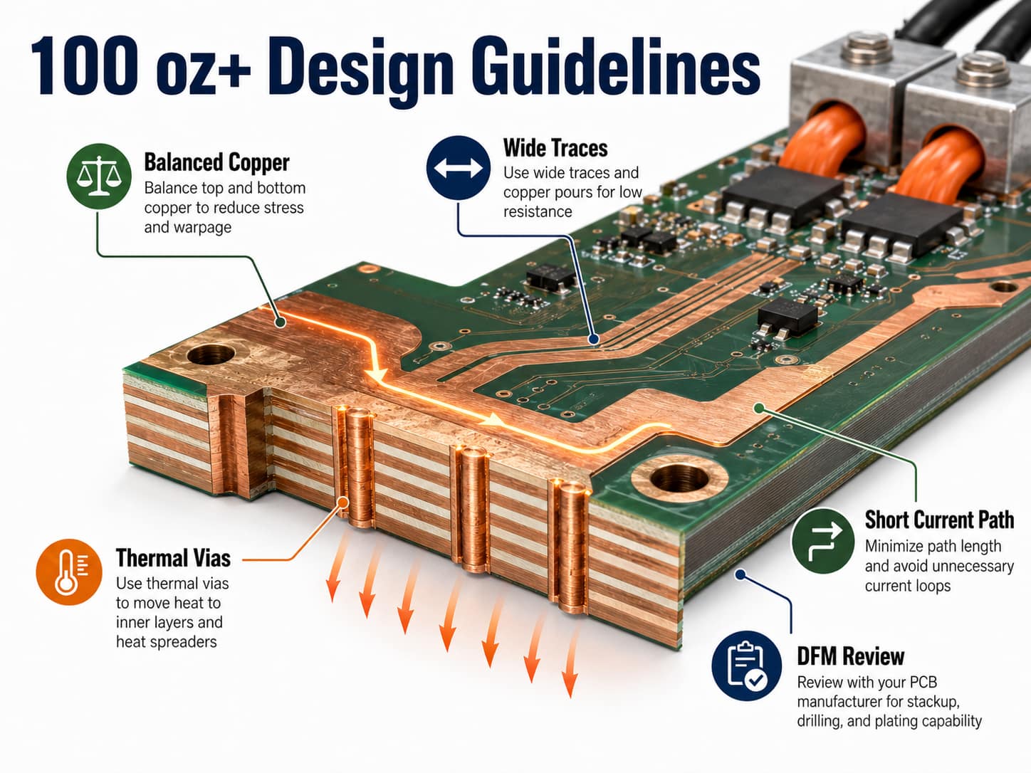
Design guidelines for 100 oz and thicker heavy copper PCBs

Key design guidelines include:

Optimize copper distribution

Large differences in copper area between layers can create lamination challenges and affect board flatness. Balanced copper distribution improves manufacturing stability.

Consider current path design

High-current paths should use:

  • Wider copper areas
  • Shorter current routes
  • Multiple copper layers when required
  • Optimized connection points

Plan thermal management early

High-power applications should consider:

  • Large copper planes
  • Thermal vias
  • Heat spreading structures
  • Component placement strategy

Complete DFM review before production

For 100 oz+ designs, customers should provide:

  • Maximum current requirement
  • Operating temperature
  • Mechanical dimensions
  • Layer stack-up preference
  • Reliability requirements

Early engineering review helps confirm whether the design is suitable for production.

Why Choose EBest Circuit for Heavy Copper PCB Manufacturing?

Selecting a heavy copper PCB supplier requires more than checking the maximum copper thickness. Manufacturing experience, engineering support, and process control directly affect final PCB reliability.

EBest Circuit provides:

  • Heavy copper PCB manufacturing capability
  • Custom multilayer PCB solutions
  • Mixed copper stack-up support
  • Engineering DFM review
  • Prototype and production support
  • PCB assembly integration capability

With more than 20 years of PCB manufacturing experience, EBest Circuit supports customers from initial design evaluation through PCB production and PCBA assembly.

For heavy copper PCB projects, contact sales@bestpcbs.com with your Gerber files, copper requirements, or application details.

Frequently Asked Questions About Heavy Copper PCBs

What copper thickness is considered a heavy copper PCB?

Heavy copper PCBs generally refer to boards using copper thickness above standard PCB levels, commonly starting from 3 oz copper and extending to much higher copper weights depending on the application.

Can you manufacture 100 oz copper PCB?

100 oz+ copper PCB requests require project-specific engineering review. Feasibility can be confirmed only after board size, layer structure, copper distribution, insulation, drilling, plating, and reliability requirements are evaluated.

What applications use heavy copper PCBs?

Heavy copper PCBs are commonly used in power supplies, battery systems, EV equipment, industrial controls, renewable energy systems, and high-current electronics.

What materials are recommended for heavy copper PCBs?

High Tg FR-4, suitable prepreg systems, and thermal management materials are commonly selected based on operating temperature and reliability requirements.

Can heavy copper PCBs include controlled impedance designs?

Yes. Controlled impedance can be considered when heavy copper layers are combined with appropriate dielectric thickness and stack-up planning.

What files are needed for heavy copper PCB quotation?

Customers should provide Gerber files, layer stack-up information, copper thickness requirements, board dimensions, quantity, and application details.

Request a Heavy Copper PCB Manufacturing Review

Whether you need a standard heavy copper PCB or want feasibility feedback on a 100 oz+ high-current concept, EBest Circuit can review your design requirements and provide manufacturing recommendations.

Send your PCB files or technical requirements to sales@bestpcbs.com for engineering evaluation and quotation.
You may also like

Heavy Copper PCB Manufacturer: Thickness, Stackup & Design Rules
Monday, August 24th, 2026

A heavy copper PCB manufacturer must control more than copper thickness. The fabrication route must support the current, thermal, mechanical and reliability requirements of boards that use substantially thicker conductors than conventional signal PCBs.

For buyers and hardware engineers, copper weight is only the starting point. Stackup balance, resin fill, trace geometry, hole structure, surface finish, board size, and acceptance criteria must be evaluated together. EBest Circuit therefore reviews each heavy-copper request against the complete fabrication package instead of treating one maximum copper number as a universal capability.

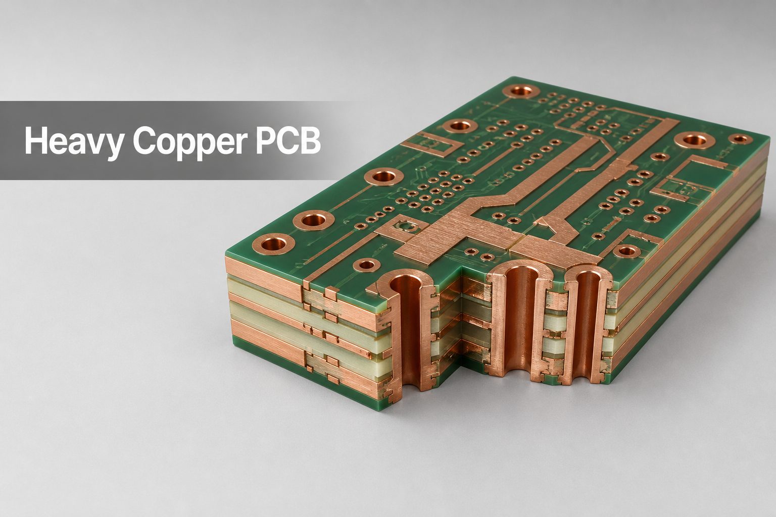
Heavy copper PCB cutaway with thick copper layers and plated through holes

What Is a Heavy Copper PCB?

A heavy copper PCB is generally understood in the PCB industry as a rigid board with copper conductors of about 3 oz/ft² or more on one or more layers. The term is not a single IPC product class, so the fabrication drawing should state the finished copper thickness required on every layer instead of relying on the words “heavy copper” alone.

Higher pcb copper weight increases the conductor cross-section available for current and heat spreading, but it also changes etching, plating, lamination, drilling, solder-mask coverage, and assembly behavior. Typical applications include power distribution, motor drives, battery systems, power converters, planar magnetics, welding equipment, industrial controls, and high-current protection circuits.

What Copper Thickness Can EBest Circuit Support?

Our current FR-4 process matrix separates routine production from special-process review. Standard designs cover inner-layer copper from 0.5 to 5 oz and outer-layer copper from 1 to 5 oz. Copper from 5 to 20 oz is listed as a special process for both inner and outer layers.

Layer position Standard process Special process Quotation status
FR-4 inner layer 0.5–5 oz 5–20 oz Confirm finished copper by layer
FR-4 outer layer 1–5 oz 5–20 oz Confirm base foil plus plating
20–200 oz extreme copper Not a standard matrix range Project-specific engineering review Stackup, size, geometry and quantity required

Our public product page describes extreme copper projects up to 200 oz. That figure should be treated as an engineering-review target, not a blanket promise that can be combined with every layer count, hole size, board dimension, material, or tolerance. A 100 oz+ request requires a dedicated feasibility review before the layout is frozen.

Which Heavy Copper PCB Stackups Are Typical?

Typical stackups keep copper mass as balanced as the electrical design allows. The exact core and prepreg construction is selected after we review copper coverage, finished board thickness, current paths, isolation requirements, hole structures, and assembly constraints.

Configuration Typical use Main DFM focus
Two-layer heavy copper Simple high-current distribution and power conversion Symmetric copper, isolation spacing and solderability
Four-layer balanced power board Separate power, ground and control functions Mirror copper weight and coverage around the centerline
Mixed-copper multilayer Heavy power layers with lighter signal layers Resin fill, lamination pressure, thickness control and registration
Extreme-copper custom construction Very high-current terminals, switches or power modules Fabrication route must be agreed before detailed layout

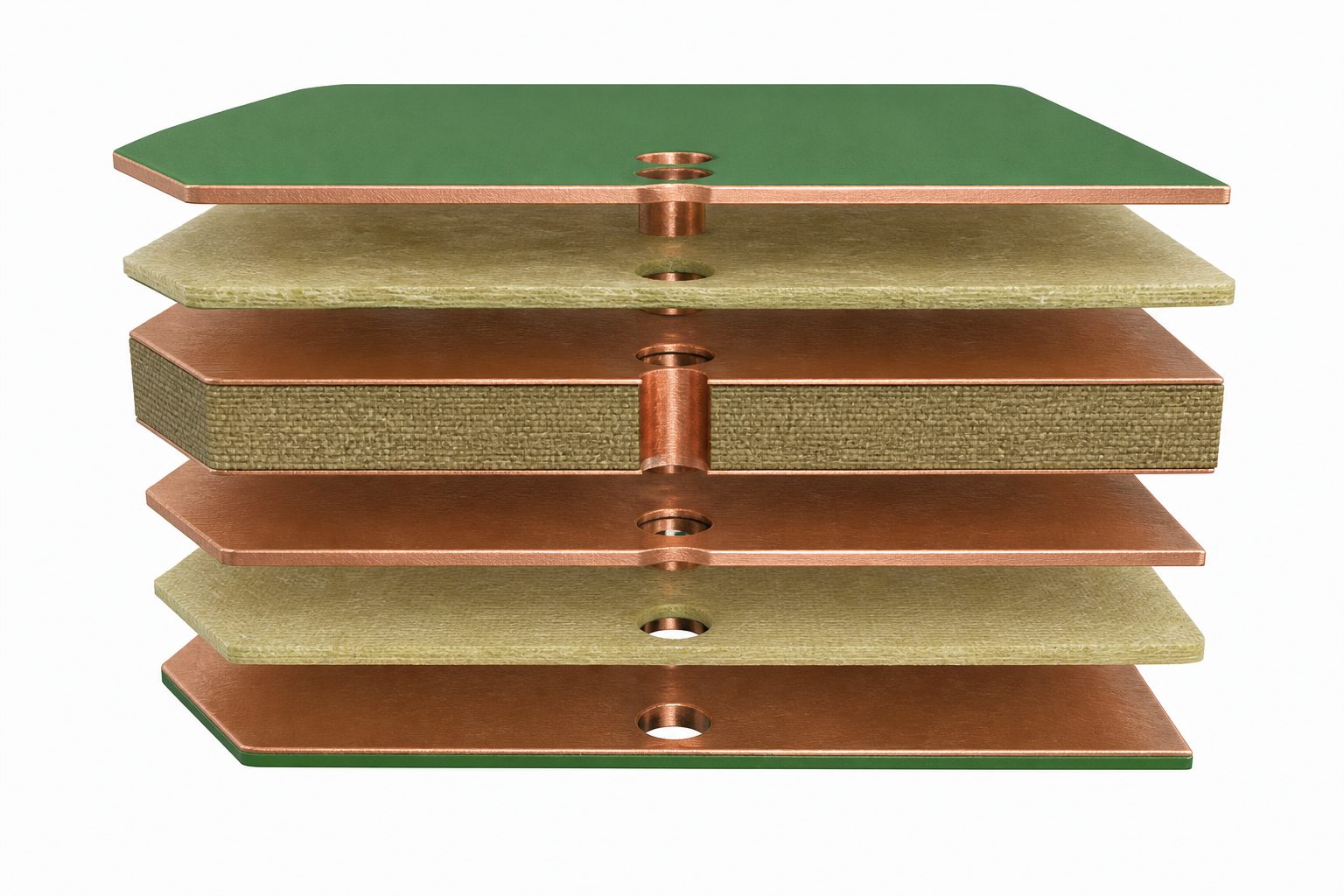
For stable heavy copper PCB design, avoid placing most of the copper mass on only one side of the stack. Large differences in copper coverage can increase resin-flow difficulty, thickness variation, bow, and twist. We may request copper balancing or thieving changes that do not alter the electrical function.

Exploded balanced multilayer heavy copper PCB stackup

Which Materials and Prepreg Systems Are Used?

FR-4 is the usual starting material, but the resin system must match the copper volume, thermal exposure, electrical requirements, and final board thickness. Our current material matrix includes low-, mid-, and high-Tg FR-4 options, with high-Tg material required for standard constructions of eight layers or more.

  • Standard FR-4 prepregs: 1080, 2116 and 7628.
  • High-Tg FR-4 examples: KB6167, ITEQ IT180, SY-S1170 and S1000-2.
  • Special material options: selected Isola, Nelco, Rogers, Taconic, PTFE and halogen-free systems, subject to stackup and procurement review.
  • Core selection: based on dielectric thickness, copper weight, required finished thickness and lamination filling demand.

Prepreg style alone does not guarantee a void-free heavy-copper build. Copper topography, remaining resin volume, pressure distribution, panel size, and copper coverage all affect fill. For deep conductor steps or 100 oz+ structures, we first review whether a conventional multilayer route is appropriate or whether a different conductor architecture is required.

Which Surface Finishes Are Available?

Available FR-4 surface finishes include OSP, HASL, ENIG, immersion silver, immersion tin, ENEPIG, hard gold fingers, and selected combined finishes. The correct option depends on pad flatness, shelf life, soldering process, contact wear, wire bonding requirements, and exposed-copper areas.

Surface finish Common selection reason Heavy-copper review point
OSP Simple solderable copper protection Handling, multiple heat cycles and exposed-copper plan
HASL / lead-free HASL Established solderable finish Surface planarity and large thermal mass
ENIG Flat pads and broad assembly compatibility Nickel/gold coverage around high copper steps
Immersion silver or tin Flat soldering surface Storage, handling and process compatibility
ENEPIG Soldering and selected wire-bonding applications Confirm bonding method and finish specification
Hard gold fingers Wear-resistant edge contacts Gold thickness, bevel and selective plating area

The finished board thickness range also varies with the selected finish. If your drawing combines thick copper with selective gold, exposed bus areas, press-fit holes, or large solder terminals, identify those regions clearly in the fabrication notes.

What Design Rules and Manufacturing Tolerances Apply?

Design rules become wider as copper thickness increases because the etching and plating window changes. Do not apply a 1 oz line/space rule to a 6, 10, or 20 oz layer. The values below are from our current FR-4 capability matrix and must still be checked against the full stackup.

Finished copper Inner standard line/space Inner special line/space Outer standard line/space Outer special line/space
2 oz 6/6 mil 5/5 mil 8/8 mil 6/6 mil
3 oz 10/12 mil 8/8 mil 12/12 mil 9/9 mil
4 oz 12/16 mil 10/10 mil 16/16 mil 12/12 mil
5 oz 16/20 mil 10/14 mil 20/20 mil 15/15 mil
6 oz 22/26 mil 14/16 mil 26/26 mil 20/20 mil
10 oz 36/40 mil 28/34 mil 40/40 mil 32/32 mil
20 oz 74/90 mil 60/80 mil 90/90 mil 70/70 mil

General FR-4 drilling tolerances in the same matrix are ±3 mil for plated-hole diameter and ±2 mil for non-plated-hole diameter under the standard process, with tighter special-process values of ±2 mil and ±1 mil respectively. Outline tolerance is typically ±5 mil. These values are not automatically combinable with maximum copper, maximum thickness, minimum holes, maximum aspect ratio, and maximum board size in one design.

Use our heavy copper PCB design guide as an early reference, then send the actual files for DFM. For current-carrying calculations, IPC-2152 relates conductor size, current and acceptable temperature rise; it does not replace thermal simulation, terminal analysis, or prototype validation for the finished assembly.

Which Via Technologies Are Available?

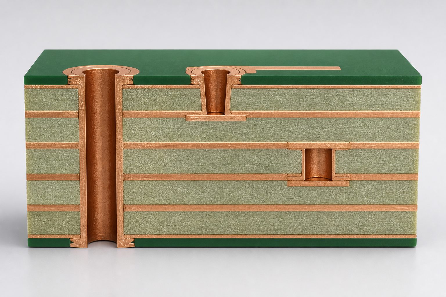
Through holes, mechanical blind/buried holes, and laser blind/buried vias are listed in our FR-4 capability matrix. The generic matrix shows 0.10 mm laser blind/buried vias, 0.20 mm standard mechanical blind/buried holes, and 0.15 mm special mechanical blind/buried holes.

  • Plated through holes: standard maximum aspect ratio 8:1; special process up to 10:1.
  • Mechanical blind/buried holes: 0.20 mm standard and 0.15 mm special-process minimums.
  • Laser blind/buried vias: 0.10 mm listed capability for suitable HDI constructions.
  • High-current transitions: multiple parallel vias, larger finished holes, thicker barrel copper, or direct copper structures may be considered after current and thermal review.

These minimums describe the broader FR-4 process range, not a guarantee that microvias can be combined with 20 oz or 100 oz copper. On heavy power layers, larger via structures and generous annular rings are usually more manufacturable. We confirm drill diameter, pad size, finished barrel copper, aspect ratio, and connection pattern together.

Cutaway showing through, blind and buried vias in a multilayer heavy copper PCB

Which Standards and Certifications Apply?

The applicable document set depends on the product class, end market, customer drawing, and purchase specification. A heavy copper board should not be described as “IPC compliant” without naming the exact document, revision, class, and acceptance requirements.

  • IPC-2152: guidance for determining current-carrying capacity from conductor size and acceptable temperature rise.
  • IPC-2221 and IPC-2222: generic and rigid-board design requirements.
  • IPC-6012F: qualification and performance requirements for rigid printed boards.
  • IPC-A-600: acceptability criteria for printed boards when called out with the applicable performance specification.

EBest Circuit company materials list ISO 9001:2015, ISO 13485:2016, IATF 16949, AS9100D, UL, RoHS and REACH documentation. Certification scope is not identical for every product, manufacturing site, or end use. State your industry and required certificate package in the RFQ so we can confirm the applicable manufacturing route and provide the relevant evidence.

What Determines Typical Lead Time?

Heavy copper lead time is quoted after DFM because the work does not follow one standard prototype schedule. The public EBest Circuit lead-time table directs special boards to contact us for project-specific timing, and that is the correct approach for heavy and extreme copper.

  • Finished copper weight on every inner and outer layer.
  • Layer count, board thickness, panel size and copper balance.
  • Laminate and prepreg availability, including special or halogen-free systems.
  • Mechanical, blind, buried or laser-via requirements.
  • Surface finish, selective plating and solder-mask build.
  • Prototype quantity, production quantity and test-coupon requirements.
  • DFM clarification cycles and customer approval time.

To shorten the schedule, submit a complete, internally consistent package and approve the proposed stackup before detailed routing is locked. You can review our general PCB lead-time framework, but the written quotation and order acknowledgement govern the actual heavy-copper delivery date.

How Should Engineers Design 100 oz+ PCBs?

A 100 oz+ board must be treated as an extreme copper PCB project, not as a 10 oz layout with every dimension multiplied. One ounce of copper per square foot is approximately 35 µm, so 100 oz represents roughly 3.5 mm of copper before considering dielectric layers, plating, surface finish, and fabrication tolerances.

  1. Define the electrical target. Provide continuous and peak current, duty cycle, allowed voltage drop, ambient conditions, cooling method and maximum temperature rise.
  2. Specify finished copper by layer. State which layers require 100 oz+ and whether the target includes plated build-up. Do not use one global copper note for a mixed construction.
  3. Separate power and signal needs. Keep fine-pitch control circuitry away from the extreme-copper geometry or place it on a separate assembly when practical.
  4. Use broad, simple conductors. Avoid fine neck-downs, dense spacing, small thermal spokes and abrupt current bottlenecks. Exact minimum geometry must come from project DFM.
  5. Minimize layer transitions. Where current must change layers, define the total current path through terminals, copper features and via structures rather than counting vias alone.
  6. Balance the construction. Keep copper mass and coverage as symmetric as possible to reduce lamination and flatness risk.
  7. Reserve mechanical space. Expect larger pads, holes, clearances, edge distances and finished board thickness than a normal PCB.
  8. Freeze the layout after fabricator DFM. We must agree on the manufacturing route, stackup, conductor geometry, tolerances, coupon plan and inspection criteria before release.

These are high current PCB design guidelines, not a released 100 oz design-rule table. EBest Circuit’s controlled FR-4 matrix currently provides numeric line/space rules through 20 oz. Any 100 oz+ geometry remains subject to engineering feasibility, material sourcing, panel constraints, and a written project-specific rule set.

What Should You Send for DFM Review and Quotation?

A complete package lets us distinguish a feasible heavy-copper build from a requirement that needs structural changes. Send the electrical requirements together with the fabrication data, not just Gerber files and a single copper number.

  • Gerber or ODB++ data, NC drill files, drill table and board outline.
  • Layer stackup with finished copper weight for every layer.
  • Finished board thickness, tolerance, dimensions and quantity.
  • Material family, Tg, CTI, flammability and halogen-free requirements where applicable.
  • Surface finish, selective plating, exposed copper and edge-contact requirements.
  • Continuous/peak current, temperature-rise limit, duty cycle and cooling conditions.
  • Required IPC document, class, test coupons, microsections, electrical test and certificate package.
  • Prototype target date and production forecast.

Our general PCB capability page provides broader reference data. For a binding decision, the reviewed stackup, DFM response and quotation take priority over standalone website maxima.

Heavy copper PCB and polished cross-section coupon under microscope inspection

FAQ About Heavy Copper PCB

Is 3 oz copper considered heavy copper?

Many PCB manufacturers use 3 oz/ft² as the practical starting point for heavy copper, although there is no single IPC definition that makes the label sufficient for fabrication. Always state the finished copper thickness required on each layer.

Can inner and outer layers use different copper weights?

Yes. Mixed-copper stackups can place heavier copper on power layers and lighter copper on signal layers. The combination must be reviewed for resin fill, copper balance, finished thickness, registration and the line/space required on each layer.

Can heavy copper PCBs use blind or buried vias?

They can in suitable constructions, but the smallest generic FR-4 via capability cannot automatically be combined with the highest copper weight. We review hole type, connection layers, annular ring, dielectric thickness and copper build together.

Does thicker copper always allow more current?

Thicker copper increases conductor cross-section, but current capacity also depends on trace width, temperature-rise limit, adjacent copper, board material, airflow, enclosure, duty cycle, terminals and layer position. Use IPC-2152 as a design reference and validate the complete assembly.

Which finish is best for a heavy copper power board?

There is no universal finish. ENIG is useful where pad flatness matters, HASL is an established solderable option, OSP is simple, and ENEPIG may support selected bonding needs. The assembly process, storage plan, contact wear and selective-plating requirements decide the finish.

Can EBest Circuit make a 100 oz PCB?

We evaluate 100 oz+ requests as extreme-copper projects. Our controlled FR-4 matrix provides standard and special rules through 20 oz, while higher public maxima require project-specific confirmation. Send the stackup, geometry, current target, board size and quantity for a written feasibility decision.

How Can EBest Circuit Support Your Heavy Copper PCB Project?

At EBest Circuit, we support heavy copper PCB stackup review, material selection, DFM, prototype fabrication, production planning, electrical testing and cross-section inspection. We will identify which requirements fit the standard process, which require a special route, and which need redesign before they become cost or reliability problems.

Send your files and operating requirements through our PCB quotation and engineering contact page. For 20 oz, 100 oz+ or mixed-copper multilayer designs, request the project-specific stackup and design rules before final layout release.

You may also like

High Current PCB Design Guidelines, Rules & Tips
Friday, November 14th, 2025

Looking for high current PCB design guidelines? Let’s discover rules and tips, layout and routing techniques, material selection, thermal solution, testing methods for high current PCB design.

Are you troubled with these questions?

  • Does your PCB overheat during full-load testing, compromising device lifespan and stability?
  • Does complex power module layout always challenge your signal integrity with interference?
  • How to ensure long-term current-carrying capacity and safety margin of high-current PCBs within budget?

As a high current PCB manufacturer, EBest Circuit (Best Technology) can provide you service and solutions:

  • Free DFM Current Path Optimization: Pre-production free DFM analysis optimizes copper thickness balance, trace width, and via arrays to enhance current capacity and thermal efficiency, eliminating overheating risks from the source.
  • Integrated Power-Thermal Co-Design: Synchronize power integrity design with thermal path planning to avoid noise interference, ensuring stable operation in high-power scenarios.
  • Cost-Controlled Reliability Solution: Leverage process expertise and material databases to recommend optimal substrate-process combinations within budget, achieving durable high-current PCBs for harsh environments.

Welcome to contact us if you have any inquiry for high current PCB design or manufacturing: sales@bestpcbs.com.

Why High Current PCB Design Is Important?

  • Reduce Thermal Failure Risk: Improperly designed high-current paths can generate localized overheating, leading to solder joint melting, substrate aging, or even interlayer delamination. Optimizing copper thickness, thermal via placement, and heat dissipation pathways distributes heat evenly, extending PCB lifespan.
  • Ensure Signal Integrity: High-current-induced electromagnetic interference (EMI) may disrupt adjacent sensitive signal lines. Proper partitioning, shielding layers, and differential pair routing minimize crosstalk, ensuring stable high-speed signal transmission to prevent system false triggers or data loss.
  • Match Current Carrying Capacity: Accurate calculation of trace width and copper thickness based on current requirements avoids bottlenecks. For instance, 10A current requires at least 40mil trace width (1oz copper thickness). Overloading raises resistance, increases voltage drop, and eventually causes localized burnout.
  • Enhance Mechanical Stability: High-current paths often involve bulky components like MOSFETs or inductors, necessitating consideration of PCB bending stress. Adding anchor vias, stiffeners, or selecting high-Tg (glass transition temperature) substrates prevents thermal expansion-induced pad cracking or interlayer separation.
  • Optimize Cost Efficiency: Precise planning of high-current paths during the design phase reduces rework costs (e.g., adding copper, supplementing heat sinks) or material upgrades (e.g., 2oz copper thickness). Reliable operation lowers maintenance frequency, improving overall product cost-effectiveness.
  • Comply With International Safety Standards: High-current designs must meet safety certifications like UL and IEC for temperature rise, flame resistance, and electrical clearances. Compliant designs avoid legal risks and ensure reliable operation in diverse environments, such as high-temperature industrial settings.
Why High Current PCB Design Is Important?

High Current PCB Design Rules & Tips

Below are rules and tips for high current PCB design:

1. Current Carrying Capacity Matching Principle

Copper Foil Parameters:

  • For 1oz copper foil (35μm) at 25℃, 10A current requires copper width ≥8mm, with each additional 1A increasing width by 0.8mm;
  • For 2oz copper foil (70μm) at 25℃, 10A requires width ≥4mm, with each additional 1A increasing width by 0.4mm;
  • For 4oz copper foil (140μm) at 25℃, 10A requires width ≥2mm, with each additional 1A increasing width by 0.2mm.
  • High Temperature Correction: For every 10℃ increase in ambient temperature, copper width must increase by 10%-15%.

Practical Tips:

  • Prioritize wide copper foil designs over multiple parallel thin copper foils.
  • For currents exceeding 30A, adopt “thickened copper” processes with local copper thickness up to 6oz.
  • Post-design verification must be performed using current-carrying simulation tools (e.g., Altium Designer current calculator).

Applicable Scenarios: All high-current scenarios, especially power device supply loops.

2. Shortest Current Path Principle

Core Requirements & Specific Parameters:

  • Path Length: Current paths must be shortened by ≥20% compared to conventional designs within the same loop.
  • Corner Requirements: 90° sharp corners are prohibited; use 45° angles or circular arcs with radius ≥1mm.
  • Via Quantity: ≤2 vias per current path, with via diameter ≥0.8mm.

Practical Tips:

  • Position power input and output terminals adjacent during layout to minimize current path length.
  • Avoid circuitous routing for high-current lines; cross small-signal areas when necessary while maintaining safety clearance.
  • Ensure full connection between via walls and surrounding copper using thermal relief structures.

Applicable Scenarios: High-current loops in motor drives, power modules, inverters, etc.

3. Thermal Distribution Balance Principle

Core Requirements & Specific Parameters:

  • Temperature Control: PCB surface temperature during normal operation must ≤60℃ (components must tolerate >85℃).
  • Heat Dissipation Structure: Heat dissipation via diameter 0.8-1.2mm, spacing 2-3mm, fully connected to copper; copper exposure area in high-current regions ≥30% of total copper area.

Practical Tips:

  • Connect high-current copper to large ground planes to reduce local current density and distribute heat.
  • Establish dedicated thermal channels for hotspots like power device pads.
  • Use infrared thermal imagers to identify hotspots and optimize designs.

Applicable Scenarios: High-temperature scenarios like new energy chargers, industrial power supplies, automotive OBCs.

4. Insulation Safety Principle

Core Requirements & Specific Parameters:

  • Clearance Requirements: For low-voltage high-current (<100V) scenarios, clearance from small-signal lines ≥5mm; For high-voltage high-current (>100V) scenarios, clearance from other circuits ≥8mm, creepage distance ≥10mm.
  • Insulation Materials: Must withstand ≥170℃ temperature and ≥2× rated voltage breakdown.

Practical Tips:

  • Implement “zoned layout” strategies to physically isolate high-current areas from small-signal areas.
  • Use FR-4 TG170 or higher specification substrates for high-voltage high-current regions.
  • Perform insulation withstand testing at 1.5× rated voltage for 1 minute before mass production.

Applicable Scenarios: Safety-critical scenarios like high-voltage inverters, energy storage systems, medical devices.

High Current PCB Design Rules & Tips

High Current PCB Layout & Routing Technique

  • Precise Calculation of Trace Width and Current Capacity: Calculate trace width using IPC-2152 standards and formulas like W=I/(k×ΔT0.5) or tools such as Saturn PCB Toolkit. For 35μm copper foil at 40°C, use k=0.048. Reserve a 30% width margin for critical paths to prevent overload from peak currents.
  • Optimized Current Path Topology: Design high-current traces with “short and straight” paths, replacing 90° corners with 45° or arc transitions to reduce inductance. Place power traces adjacent to ground planes to form low-impedance loops, minimizing EMI interference.
  • Parallel Via Array Design: Deploy 5-10 Φ0.3mm vias in parallel at power/ground plane connections. Verify single-via current capacity at 0.5A/0.3mm² and maintain via spacing ≥1mm to avoid thermal stress concentration and ensure uniform current distribution.
  • Copper Thickness Gradient Matching: Select copper thickness based on current requirements: 35μm (1oz) for ≤3A, 70μm (2oz) for ≤6A. For higher currents, use multi-layer parallelism or localized thick copper, with a 20% thermal design margin.
  • Signal-Power Isolation Strategy: Maintain ≥3mm spacing between high-current traces and sensitive signals, with ground planes in between. Enclose differential pairs/high-speed signals with GND to prevent overlap with power layers and reduce crosstalk.

Material Selection Guide for High Current PCB Design

1. Copper Foil Thickness Selection

  • Standard and Scenario: High-current paths prioritize copper foil thickness of 2oz (70μm) or higher, such as 3oz (105μm) or 4oz (140μm), to enhance current-carrying capacity and thermal dissipation. 1oz (35μm) is suitable for conventional circuits, while ultra-thin foil (0.5oz) is limited to high-frequency/precision signal lines.
  • Design Considerations: Annotate “outer layer finished copper thickness” (e.g., 2oz) in designs and control trace width accuracy via etching compensation. IPC-4562 specifies a ±10% copper thickness tolerance; confirm process capabilities with manufacturers.

2. Substrate Material Types

  • Metal Core Substrates: Aluminum substrates (cost-effective, excellent thermal dissipation) are ideal for LEDs and power modules. Copper substrates (superior thermal conductivity) are used in automotive electronics and high-power devices but require oxidation protection and cost consideration.
  • High-Temperature Epoxy: Optimize for high-temperature epoxy resins (e.g., FR4-H grade) with Tg >170°C for automotive and military applications. Avoid standard FR4 (Tg 130–140°C) for prolonged operation above 150°C.
  • High-Frequency/Specialty Substrates: For 5G/mmWave applications, combine Rogers RO4000 series (low dielectric loss) with metal substrates. Prioritize current-carrying and thermal performance in high-current scenarios, using high-frequency materials only locally.

3. Insulation Layer and Thermal Management

  • Thermal and Dielectric Performance: Use ceramic-filled polymers (e.g., AlN with CTE 4–5ppm/°C) or high-thermal-conductivity epoxy glass cloth (80–100μm thick) to match the CTE of copper substrates (16.5ppm/°C) and components, reducing thermal stress and delamination risks.
  • Thermal Expansion Matching: Address CTE mismatch between silicon chips (2.6ppm/°C) and copper substrates via graded CTE insulation layers or buffer layers (e.g., low-CTE polymers) to prevent solder joint cracking.

4. Process and Cost Optimization

  • Cost Optimization: 1oz copper foil + FR4 for consumer electronics; 2oz copper foil + aluminum substrate for industrial/power equipment; 0.5oz copper foil for ultra-compact devices (e.g., earbuds).
  • Process Adaptation: Thick copper foil increases etching difficulty, requiring trace width compensation. Metal substrates need specialized drilling/milling equipment to avoid edge burrs or delamination from standard FR4 processes.

5. Reliability Verification

  • Thermal Cycling Tests: Validate solder joint and insulation layer durability via -40°C to 125°C thermal shock tests (ASTM D149). High-power scenarios require additional mechanical shock testing (IEC 60068-2-27).
  • Standards Compliance: Adhere to IPC-6012 (rigid PCB performance) and UL 94 V-0 (flammability certification). Ensure materials pass third-party testing for temperature resistance and dielectric properties.

Thermal Management Solutions for High Current PCB Design

  • Use high-thermal-conductivity substrates: Prioritize aluminum-core PCBs (thermal conductivity: 200-400 W/m·K) or copper-core PCBs, which significantly outperform standard FR4 (0.3 W/m·K) in heat dissipation. For high-density designs, opt for modified FR4 with thermal conductivity ≥3.0 W/m·K, combined with embedded copper blocks or thermal via arrays to enhance localized heat dissipation.
  • Optimize current path layout: High-current paths should follow the “short, wide, thick” principle. Route length should be minimized, copper width ≥2x current-carrying requirement (per IPC-2152), and copper thickness ≥2oz (70μm) to reduce resistive heating. Critical power loops should use parallel traces or copper pours to distribute current density and prevent localized overheating.
  • Implement thermal-mechanical co-design: Place dense thermal vias (≥10 vias/cm², 0.3-0.5mm diameter) beneath power devices (MOSFETs, IGBTs) to transfer heat from inner layers to outer cooling layers. Use solid copper planes or thermal grids as cooling layers, connected to device pads via multiple thermal vias to form a 3D heat dissipation network. For BGA packages, add thermal rings around pads linked to cooling vias to reduce junction-to-board thermal resistance.
  • Integrate active cooling structures: Design fins or heat sink attachment points at PCB edges or unused areas for passive cooling. For high-power modules (≥50W), include embedded heat pipe or vapor chamber interfaces connected to PCB thermal channels via soldering or press-fit. Reserve airflow channels in ventilation paths to guide airflow and remove heat.
  • Validate with thermal simulation and testing: Use thermal simulation tools (ANSYS Icepak, FloTHERM) to model 3D thermal behavior, inputting device power, ambient temperature, and cooling conditions to simulate steady-state/transient temperature distributions. Ensure hotspots (e.g., power device pads, high-current traces) remain below 80% of substrate glass transition temperature (Tg). Post-design, verify thermal performance via thermal imaging (e.g., FLIR) and compare with simulation results to validate effectiveness or iterate layout/cooling structures as needed.
Thermal Management Solutions for High Current PCB Design

Common Mistakes to Avoid in High Current PCB Design

Seven common mistakes to avoid in high current PCB design:

Insufficient Trace Width Causing Voltage Drop and Overheating

  • Problem: Power traces not designed according to current requirements, e.g., 10A current requires at least 2.5mm width (1oz copper thickness), leading to voltage drop or localized overheating.
  • Solution: Calculate trace width using IPC-2221 formula I=k×ΔT0.44×A0.65, where k=0.024 for 1oz copper, ΔT is allowable temperature rise (e.g., 10°C), and A is cross-sectional area (mm²). For 40A with 2oz copper, A≈5.0mm2 requires 5mm width. Use parallel traces on dual-layer PCB with ≤1mm spacing and via arrays (≤5mm pitch) for double current capacity.

Missing Thermal Path Causing Thermal Failure

  • Problem: High-power components (e.g., MOSFETs) lack thermal vias or copper under pads, causing thermal stress concentration.
  • Solution: Implement a 3-layer thermal design: copper pad + thermal vias + heatsink. Place ≥0.3mm via arrays (spacing ≤1mm) under power device pads, connecting to inner thermal layers (e.g., layer 2 or N-1) and edge thermal rails or metal cores. Use ≥2oz copper for thermal layers with ENIG or OSP surface finish for better thermal conductivity. Validate thermal resistance path via simulation to ensure total junction-to-ambient thermal resistance ≤10°C/W.

Insufficient Via Current Capacity

  • Problem: Standard 0.3mm via supports only 1A current, causing bottleneck failures in high-current paths.
  • Solution: Use Via-in-Pad with copper fill or increase via size to 0.6mm, with ≥3 vias in parallel for current sharing. In multi-layer PCBs, alternate power-ground via stacks to form low-impedance vertical paths with ≤2mm via spacing. Ensure HASL or immersion silver finish for full solder fill and low contact resistance. Verify via current density, e.g., 0.6mm via with 2oz copper supports 3A.

“Dumbbell” Power Plane Layout

  • Problem: Power planes fragmented by signal traces, creating high-current density hotspots and excessive voltage drop.
  • Solution: Adopt dual-layer power-ground sandwich with ≤10mil spacing for planar capacitance. Use ≥20mil wide power channels to avoid single-layer long-distance transmission. For high-current zones (e.g., DC-DC outputs), combine power planes, channels, and decoupling capacitors (≥100μF, ESR≤10mΩ) near loads. Utilize “Plane Clearance” tools in Allegro/Altium to auto-detect and fix plane fragmentation.

EMC Issues: Ground Plane Fragmentation and Noise Coupling

  • Problem: Split ground planes create ground bounce or loop antennas, causing EMI violations.
  • Solution: Implement star grounding for sensitive circuits (e.g., ADCs) to isolate them from digital grounds. Place Y-capacitors across common-mode chokes with impedance matching (e.g., 100Ω). For HF noise, use double-layer ground-shield structure with grounded shield covering sensitive areas. Validate via near-field probe scans to ensure ≤30dBμV/m radiation at 10m.

Manufacturing Defects: Pad Design and DFM

  • Problem: Solder mask-covered pads or dimensional errors cause poor soldering or shorts.
  • Solution: Use NSMD (Non-Solder Mask Defined) pads with 20% larger size than component leads (e.g., 0.72mm pad for 0.6mm wide 0603 resistor). Keep silkscreen ≥0.2mm from pads. For BGAs, route “dog-bone” traces to vias outside pads. Run DRC/ERC checks with DFM tools to ensure trace/space ≥ manufacturer limits (e.g., 6mil) and verify pad-mask alignment.

Signal Integrity: Impedance Mismatch and Crosstalk

  • Problem: Unmatched impedance in high-speed traces (e.g., DDR) causes reflections or crosstalk.
  • Solution: Design 50Ω microstrips with 4-6mil dielectric thickness and εr=4.2-4.8. Use serpentine routing for length matching (bending radius ≥3× width, spacing ≥2× width). Isolate sensitive traces (e.g., clocks) from power lines by ≥3× width with ground shielding. Simulate eye diagrams to ensure eye width ≥40% period and eye height ≥800mV. For differential pairs, use tight coupling (spacing ≤2× width) with 90-100Ω impedance control.

Why Partner With Us for Your High Current PCB Design & Manufacturing?

Reasons to partner with us for your high current PCB design and manufacturing:

  • Free DFM (Design for Manufacturability) Analysis: Pre-production DFM evaluations identify potential issues in pad dimensions, trace spacing, and thermal design, enabling proactive optimization to avoid cost overruns and delays.
  • Global Certifications for High-Reliability Compliance: Certified with ISO 9001 (quality management), IATF 16949 (automotive), ISO 13485 (medical), and RoHS (environmental compliance), meeting stringent requirements for medical, automotive, and industrial sectors.
  • 19 Years of High-Current PCB Expertise: With 19 years of specialized experience, we master core technologies such as ≥6oz copper thickness, microvia plating, and thermal management optimization, addressing high-current challenges like heat dissipation and signal integrity.
  • Cost-Sensitive Pricing Solutions: We provide competitive pricing through material optimization, design simplification, and bulk procurement, ensuring 15%-30% cost reduction for budget-sensitive projects.
  • 24-Hour Rapid Prototyping for Urgent Orders: Urgent orders benefit from 24-hour prototype delivery, enabling swift design validation and accelerated time-to-market.
  • 99.2% On-Time Delivery Rate: Leveraging intelligent supply chain management and lean production, we achieve a 99.2% on-time delivery rate, minimizing production delays and inventory risks.
  • 100% Batch Inspection & Strict Quality Control: Batch products undergo 100% full inspection with six-stage quality checks including AOI optical inspection and electrical testing, ensuring ≥99.8% yield and reduced post-sale costs.
  • Customized Technical Solutions: Tailored stack-up design, impedance control, and high-frequency material selection ensure optimal performance-cost balance for high-current, high-power applications, meeting unique client requirements.

Welcome to contact us if you have any request for high current PCB design or manufacturing: sales@bestpcbs.com.

You may also like