PCB manufacturing PCB manufacturing
Home > Blog

automated optical inspection working principle

Automated Optical Inspection (AOI) for PCB: Process, Defects, and Limitations
Friday, July 31st, 2026

automated optical inspection (AOI) is a non-contact inspection method used in bare PCB fabrication and PCBA assembly. It combines industrial cameras, controlled lighting, motion hardware, and image-processing software to identify visible defects.

For bare boards, AOI checks copper patterns, pads, spacing, and etched features. For assembled boards, it verifies component presence, orientation, placement, polarity, and visible solder quality.

AOI is fast and repeatable, but it does not prove that a board works electrically. It cannot see hidden BGA joints, measure resistance, confirm firmware, or validate product performance. Buyers should therefore treat AOI as one layer of a wider inspection plan rather than a complete quality guarantee.
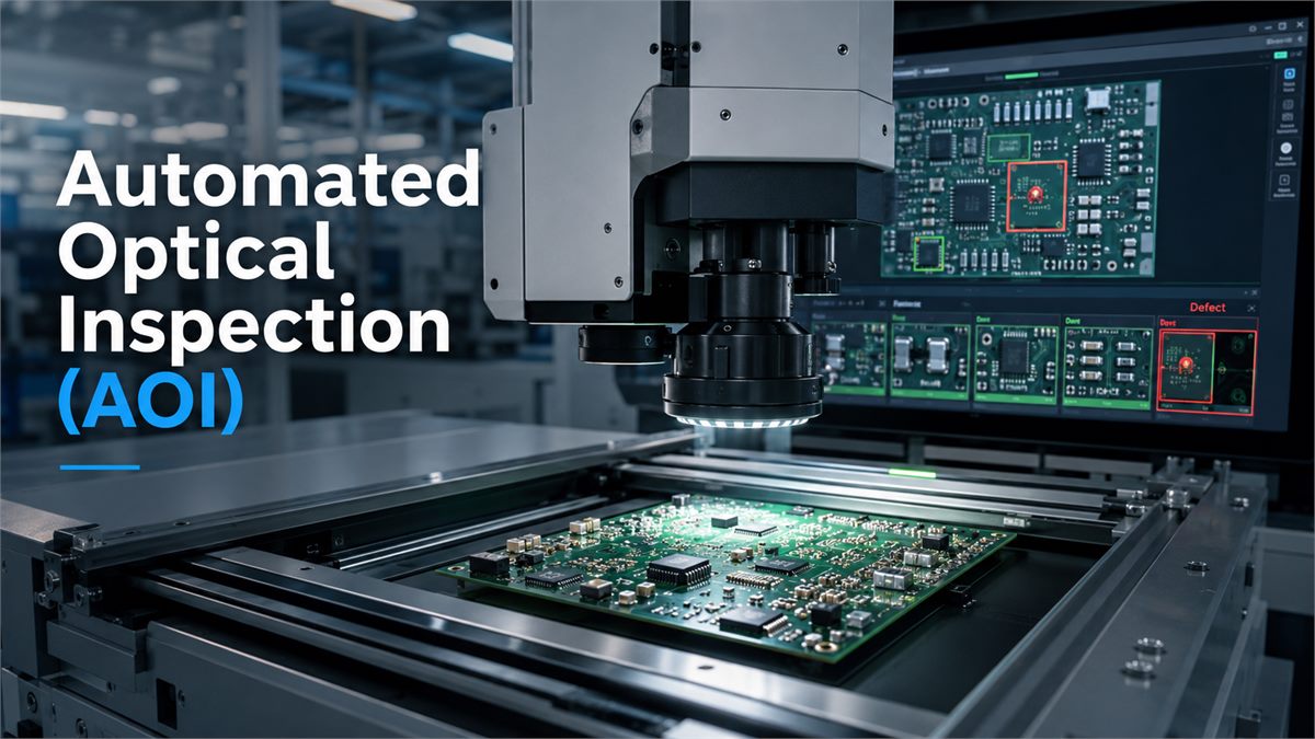
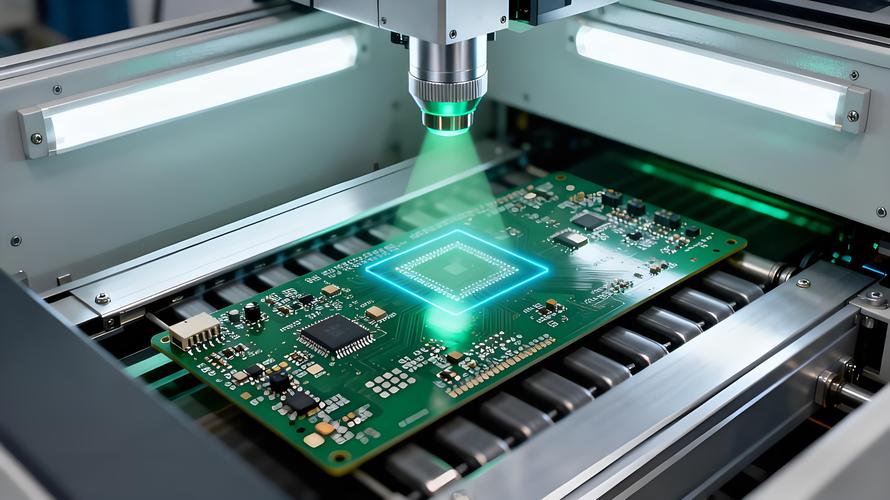
Automated optical inspection machine scanning a populated PCB assembly

What Is Automated Optical Inspection?

Automated optical inspection compares images of a PCB or PCBA against programmed reference data. That reference may come from Gerber data, CAD files, component libraries, dimensional rules, or a verified golden board.

Unlike manual visual inspection, AOI applies the same inspection logic to every board. It can check thousands of features without asking an operator to scan the entire assembly by eye.

The terms automated optical inspection and automatic optical inspection are commonly used for the same process. In electronics manufacturing, both usually refer to AOI equipment installed in a PCB fabrication or SMT line.

How Does Automated Optical Inspection Work?

The automated optical inspection working principle follows a straightforward sequence:

  • The board enters the inspection area and is positioned by a conveyor, fixture, or motion platform.
  • Controlled lighting highlights component edges, markings, solder fillets, copper traces, and surface irregularities.
  • Cameras capture 2D images or, in a 3D system, image and height data.
  • Software checks position, color, shape, rotation, height, contrast, and solder coverage.
  • Results are compared with programmed tolerances.
  • Suspect locations are sent to an operator for confirmation.
  • Inspection results may be linked to a batch number or board serial number.
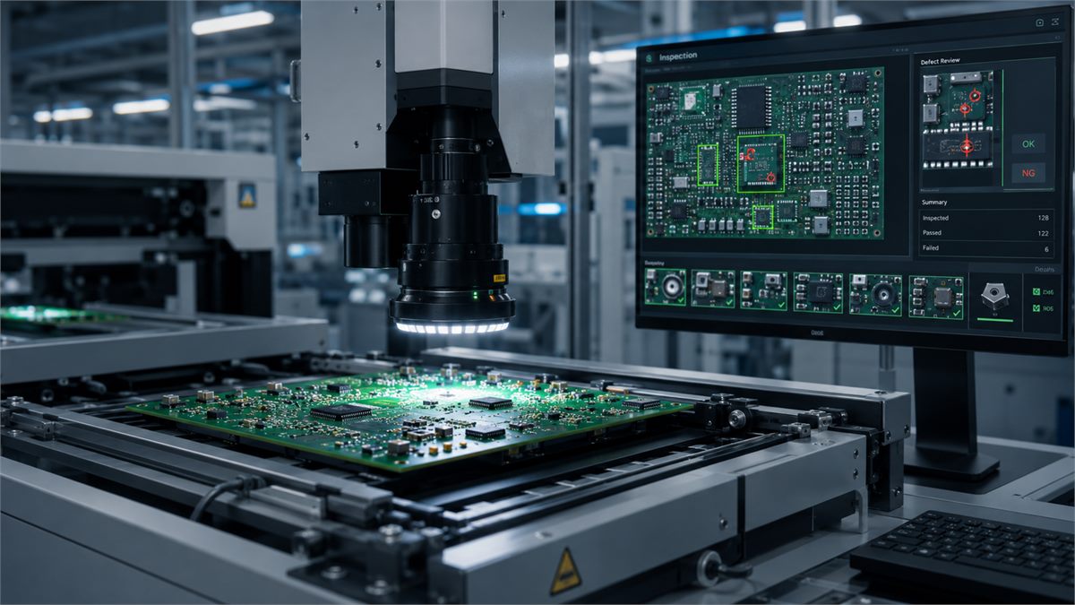
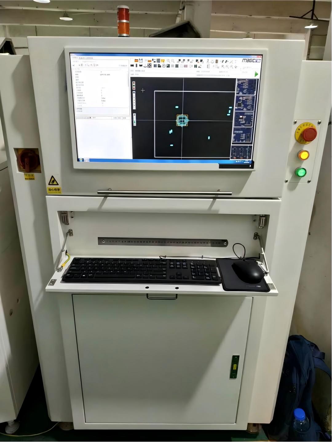
AOI inspection head scanning a PCB while software reviews detected defects

The quality of the result depends heavily on programming. If tolerances are too tight, the system creates excessive false calls. If they are too loose, real defects can pass. Reliable AOI depends as much on a well-built inspection library as it does on camera resolution.

Manufacturers generally program AOI in one of three ways:

  • CAD-based programming imports design and placement data, making it efficient for new products.
  • Golden-board programming learns from a verified assembly, although the reference board must be checked carefully.
  • Library-based programming uses stored component dimensions, polarity references, and inspection rules.

In practice, production lines often combine all three and then refine the limits during first-article inspection.

What Components Make Up an AOI System?

Automated optical inspection systems normally include the following elements:

  • Industrial cameras: Capture the board surface at a resolution suitable for the smallest inspected feature.
  • Inspection lenses: Control focus and image distortion. Telecentric lenses are useful where dimensional accuracy matters.
  • Controlled lighting: Uses direct, coaxial, side, ring, or multi-angle lighting to reveal different surface conditions.
  • Motion hardware: Positions the board and camera consistently.
  • Inspection software: Defines inspection windows, tolerances, component models, and defect rules.
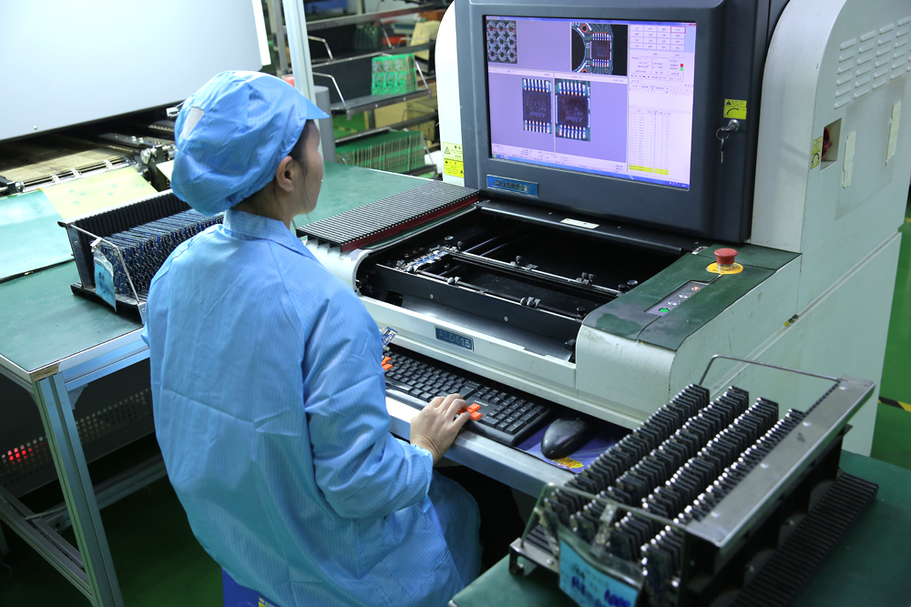
  • Review station: Allows an operator to confirm defects and classify false calls.
  • Traceability interface: Stores images, board IDs, inspection results, and process records.

Higher camera resolution does not automatically produce better inspection. Poor lighting, board movement, inaccurate component data, or weak programming can still undermine the result.

Where Is AOI Used in PCB Manufacturing?

AOI can be installed at several production stages.

Inner-Layer Bare PCB Inspection

Before multilayer lamination, AOI checks etched inner layers for opens, shorts, copper residue, missing features, and dimensional deviations. Catching a defect here prevents a bad inner layer from being laminated into a finished board.

Outer-Layer Bare PCB Inspection

After outer-layer etching, AOI compares visible traces, pads, clearances, and copper geometry with the design data.

Pre-Reflow PCBA Inspection

Pre-reflow AOI checks whether components are present, correctly placed, and properly oriented before the solder paste melts. It can reduce rework, but it cannot assess the final solder joint.

Post-Reflow PCBA Inspection

Post-reflow AOI is the most common arrangement in SMT assembly. It checks component position, polarity, tombstoning, lifted leads, bridges, and visible solder fillets after reflow.

Its location also makes the data useful for process control. For example:

  • Repeated solder bridges may point to excessive solder paste or stencil issues.
  • Recurring component shifts may indicate feeder, placement, or reflow problems.
  • Frequent polarity errors may reveal incorrect placement data or feeder setup.

AOI provides more value when defect trends are reviewed by line, product, and batch rather than handled as isolated inspection failures.

Through-Hole and Wave-Solder Inspection

AOI may inspect visible lead presence, component orientation, solder bridges, and solder coverage. Dense connectors, tall parts, and shadowed joints may still require manual or X-ray inspection.

What Bare PCB Defects Can AOI Detect?

Bare PCB AOI focuses on visible copper geometry.
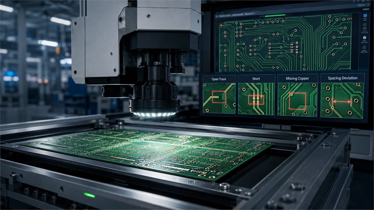
Bare PCB AOI identifying open traces, shorts, missing copper and spacing deviations
Defect What AOI identifies
Open circuit Broken or incomplete trace
Short circuit Unwanted copper between conductors
Copper protrusion Copper extending beyond the intended pattern
Missing copper Incomplete pad, annular feature, or trace
Trace-width deviation Conductor outside the programmed width limit
Spacing violation Clearance below the programmed value
Pinhole Small unwanted opening in a copper area
Etching residue Copper left where it should have been removed
Incomplete pad Missing or malformed pad geometry
Surface scratch Visible damage across copper or laminate

AOI can flag a suspected open or short, but bare-board electrical testing is still required. Optical inspection sees the surface pattern; PCB testing confirms continuity and isolation.

What PCBA Defects Can AOI Detect?

On an assembled board, AOI checks both components and visible solder joints.
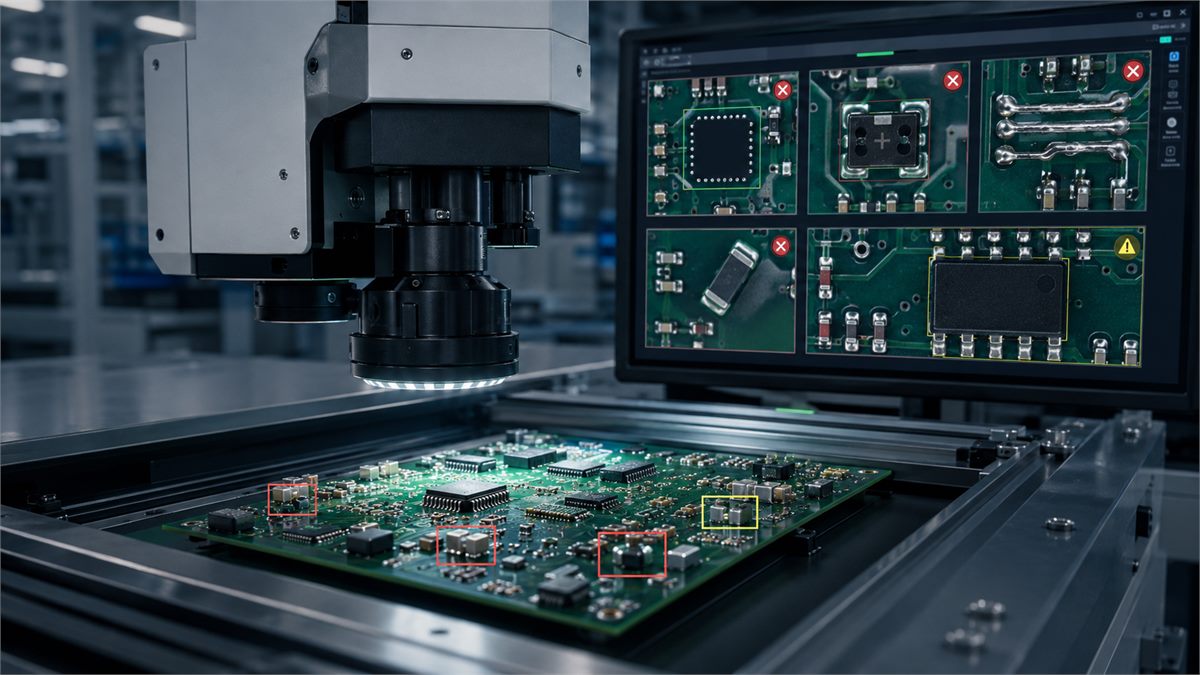
PCBA AOI highlighting missing, reversed, misaligned and solder-related defects

Component-Related Defects

Common findings include:

  • Missing or misplaced components
  • Excessive rotation
  • Reversed polarity
  • Wrong package type
  • Tombstoned or billboarded passive components
  • Lifted gull-wing leads
  • Shifted connectors
  • Incorrect IC, diode, or capacitor orientation

AOI may read top markings, but this is not always dependable. Equivalent parts can carry different codes, while small, reflective, or faint markings may be difficult to capture consistently.

Visible Solder Defects

AOI can also flag:

  • Solder bridges
  • Insufficient or excessive solder
  • Open visible joints
  • Poorly wetted leads
  • Solder balls
  • Irregular solder fillets
  • Lifted leads

Detection confidence depends on visibility. A gull-wing lead is easier to inspect than a joint hidden below a QFN, LGA, or BGA.

2D AOI vs. 3D AOI: What Is the Difference?

The practical question is whether the application needs image comparison only or actual height measurement.
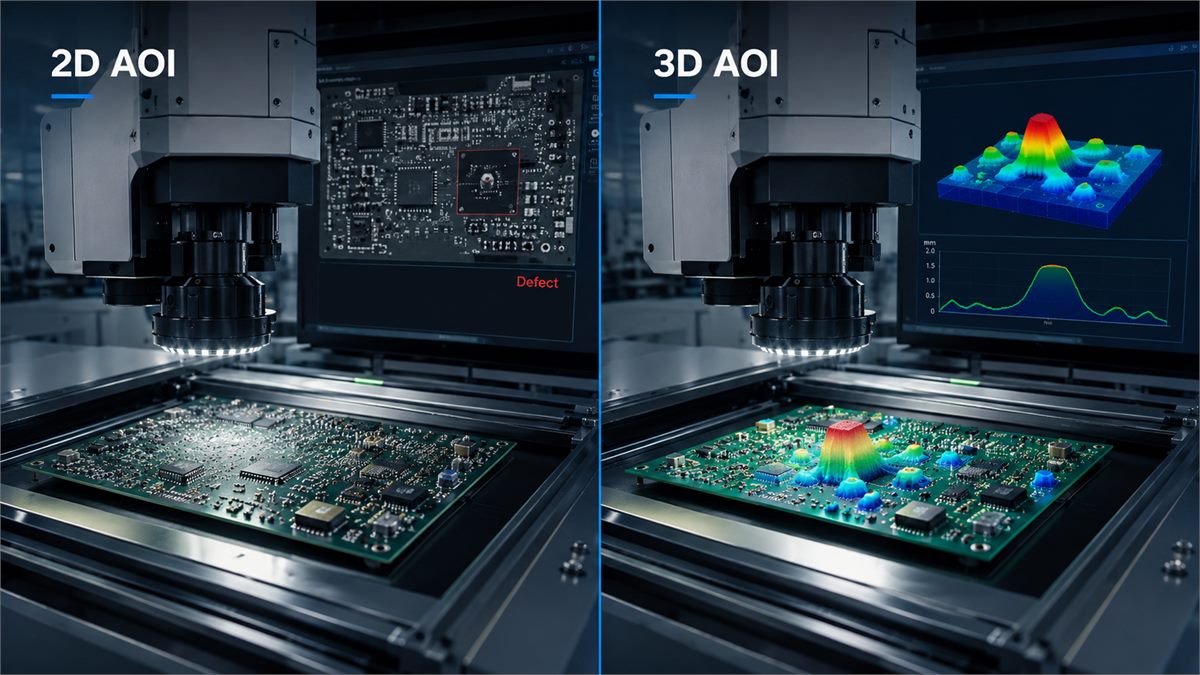
Side-by-side comparison of 2D AOI image inspection and 3D AOI height measurement
Comparison 2D AOI 3D AOI
Main data Flat surface image Image plus height profile
Presence and position Yes Yes
Rotation and polarity Yes Yes
Height measurement Limited Yes
Lifted-lead detection Lighting-dependent Usually more reliable
Coplanarity Limited Measurable
Solder profile Limited Better characterization
Programming effort Lower Higher
Equipment cost Lower Higher
Best fit Standard SMT assemblies Fine-pitch or complex assemblies

A stable product with visible joints may not need 3D AOI. It becomes more useful for lifted leads, coplanarity, board warpage, and height-sensitive defects.

It still cannot see through a package, so 3D AOI does not replace X-ray inspection.

What Can AOI Not Detect?

AOI is restricted by line of sight. It cannot directly verify:

  • Hidden BGA or LGA solder joints
  • Voids under QFNs or thermal pads
  • Internal PCB layer defects
  • Cracks inside plated holes
  • Internal via-barrel defects
  • Electrically incorrect but visually identical components
  • Firmware problems
  • Intermittent electrical faults
  • Power-sequence or signal-integrity failures
  • Functional performance
  • Long-term reliability under heat, vibration, humidity, or load

A resistor can be present and well soldered yet still have the wrong value. A BGA may look correctly placed while containing an open joint underneath. These risks require electrical testing, X-ray, functional testing, or reliability testing.

AOI vs. SPI, X-Ray, ICT, and Functional Testing

Each inspection method answers a different question.
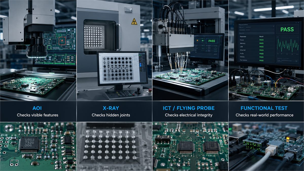
AOI, X-ray, ICT flying probe and functional testing compared in a PCBA inspection plan
Method Main target Typical stage
SPI Solder paste height, area, position, and volume After printing
AOI Visible components and solder joints Before or after reflow
X-ray or AXI Hidden solder joints and voids After reflow
ICT Nets and component-level electrical faults After assembly
Flying probe Continuity, isolation, and selected values Prototype or low volume
Functional test Powered product behavior Final test

The right plan depends on package type, board density, product risk, production volume, and customer requirements.

A simple prototype with visible joints may need AOI plus flying-probe testing. A dense BGA assembly may also require X-ray and functional testing. Adding every inspection method to every project increases cost without necessarily improving the decision value.

What Causes False Calls and Missed Defects in AOI?

False calls and missed defects usually come from a small group of process issues:

  • Reflective surfaces: Solder, shields, and exposed metal can change appearance with the lighting angle.
  • Component variation: Approved parts may differ in color, marking, edge shape, or finish.
  • Board warpage: Changes focus, height readings, and apparent component position.
  • Tall components: Create shadows around nearby parts and solder joints.
  • Weak libraries: Incorrect body dimensions, polarity references, or lead locations cause repeated errors.
  • Poor tolerance settings: Tight limits reject good boards, while loose limits allow defects through.
  • Golden-board mistakes: A flawed reference board can normalize an actual defect.
Practical rule: A useful AOI program is not the one that reports the most defects. It is the one that separates real faults from normal production variation with minimal review time.

What Are the Benefits of AOI in PCB Quality Control?

AOI is most valuable when its data is used to improve the process, not merely sort boards at the end.

Key benefits include:

  • Consistent inspection criteria across every board
  • Faster detection of recurring placement or solder problems
  • Full-board coverage without relying entirely on manual inspection
  • Clear defect images for troubleshooting
  • Better traceability by batch or serial number
  • Yield data for stencil, feeder, placement, and reflow analysis
  • Less downstream rework when faults are found early

The return depends on how well the inspection program is maintained. An AOI machine that produces a high false-call rate can slow production and distract reviewers from real defects.

How Should PCB Buyers Evaluate AOI Capability?

Asking whether a supplier “has AOI” is not enough. Buyers should ask how the equipment will be used for their specific board.

Useful questions include:

  • Is AOI applied to bare PCBs, assembled PCBAs, or both?
  • Is inspection performed before reflow, after reflow, or at both stages?
  • Is the system 2D or 3D?
  • What component sizes and feature dimensions can it inspect reliably?
  • How are false calls reviewed and recorded?
  • Are images linked to serial numbers or production batches?
  • Can AOI records be supplied?
  • How are BGA, QFN, and LGA joints checked?
  • Is X-ray available for hidden joints?
  • Can AOI be combined with flying probe, ICT, programming, or FCT?
  • Which workmanship standard and acceptance criteria are used?

A supplier cannot price meaningful AOI, X-ray, or electrical testing from Gerber data alone. Customers should provide:

  • Gerber or ODB++ data
  • BOM with manufacturer part numbers
  • Pick-and-place file
  • Assembly drawing
  • Polarity and orientation notes
  • Approved component substitutions
  • Required inspection standard
  • X-ray and electrical test requirements
  • Traceability or report requirements
  • Order quantity and delivery target

For PCB prototypes, ask whether AOI programming is included in the assembly charge and whether a formal report is required. A one-off, two-board build may not justify a detailed custom AOI report. A 50-piece pilot run, however, can benefit from recorded defect data before volume release.

Fine-pitch ICs, polarized parts, dense connectors, and bottom-terminated packages should be identified during quotation because they influence the inspection route.

At EBest Circuit, we can combine AOI with SPI, X-ray, flying-probe testing, ICT, programming, or functional testing according to the package mix and customer files. The aim is not to add every inspection method, but to cover the actual risks in the design.

FAQs About Automated Optical Inspection

Is AOI the same as visual inspection?

No. Both methods examine visible conditions, but AOI uses programmed cameras, lighting, and software to inspect predefined locations. Manual visual inspection depends more heavily on operator experience and attention.

Is automated optical inspection destructive?

No. AOI is a non-contact, non-destructive inspection method. It captures surface images without cutting, stressing, or electrically powering the board.

When is AOI performed in PCB assembly?

AOI may be performed after component placement and before reflow, but post-reflow inspection is more common. Some production lines use both positions for high-risk or high-volume assemblies.

Can AOI inspect BGA solder joints?

It can verify the BGA package position, orientation, marking, and visible perimeter conditions. It cannot inspect solder balls hidden underneath the package. X-ray inspection is normally required for those joints.

What is the difference between 2D and 3D AOI?

A 2D system analyzes flat surface images. A 3D system also measures height and surface geometry, making it more capable of detecting lifted leads, coplanarity problems, and irregular solder profiles.

Can AOI detect incorrect component values?

Sometimes, but not reliably in every case. AOI may identify a value from readable component markings. It cannot electrically measure an unmarked component or distinguish visually identical parts with different values.

Does AOI replace X-ray inspection?

No. AOI examines visible surfaces, while X-ray inspection reveals hidden solder joints and internal package features. The two methods address different defect risks.

Does AOI replace electrical testing?

No. AOI cannot confirm circuit continuity, resistance, voltage, firmware behavior, or product function. Electrical testing is still needed when those requirements matter.

What is the difference between SPI and AOI?

SPI measures solder paste before component placement. AOI checks component placement and visible solder conditions before or after reflow.

Is AOI suitable for PCB prototypes?

Yes. AOI can identify assembly errors quickly, especially on prototypes with fine-pitch or polarized components. However, programming effort and inspection cost should be considered for very small quantities. Flying-probe testing or targeted X-ray may provide greater value for certain prototype designs.

Conclusion

Automated optical inspection is effective for visible copper, placement, polarity, and solder defects, but it cannot verify hidden joints or electrical performance. Buyers should evaluate where AOI is used, whether the system is 2D or 3D, how false calls are handled, and which additional tests cover the remaining risks.

For an inspection plan and quotation, send your Gerber files, BOM, pick-and-place data, test requirements, and order quantity to sales@bestpcbs.com.

You may also like

Automated Optical Inspection PCB – Advanced AOI for PCB Production
Thursday, March 5th, 2026

Automated optical inspection PCB solutions provide fast, accurate defect detection for PCBs, ensuring high quality and reliability in electronic manufacturing.

Automated Optical Inspection PCB – Advanced AOI for PCB Production

Automated optical inspection, commonly known as AOI, is a powerful inspection method that uses cameras, lighting systems, and software to check PCBs quickly and accurately. It plays a critical role in modern PCB assembly lines where thousands of boards are produced every day. With advanced imaging and intelligent analysis, AOI systems help detect defects early and improve production efficiency.

What is automated optical inspection PCB?

Automated optical inspection PCB refers to a computer-controlled inspection method used to evaluate printed circuit boards during manufacturing and assembly. The system uses high-resolution cameras and special lighting to capture images of a PCB and then compares those images with a predefined reference.

Instead of relying on manual inspection, AOI systems analyze each board automatically. The software checks component placement, solder joints, polarity, and other details to ensure every board matches the design requirements.

In modern electronics manufacturing, PCB automated optical inspection systems are widely used after solder paste printing, after component placement, and after soldering. Each inspection stage focuses on different aspects of board quality.

The inspection process usually involves several core elements:

  • High-resolution cameras for image capture
  • Precision lighting systems for contrast and clarity
  • Image processing software to analyze patterns
  • A comparison database containing the reference design
  • Automatic defect classification tools

These systems allow factories to inspect thousands of boards every hour. The process is fast, consistent, and reliable. Because inspection results are stored digitally, engineers can also trace production issues and improve process control.

How does automated optical inspection work for PCBs?

The automated optical inspection working principle is based on advanced imaging and pattern comparison. The system captures images of the PCB and analyzes them with specialized software to detect differences from the expected design.

The inspection begins when a PCB enters the AOI machine on a conveyor. Cameras scan the entire board while controlled lighting highlights components and solder joints. The captured images are then processed by inspection software. The system compares the captured images with reference data generated from PCB design files or a known good board. When differences appear, the system flags them as potential defects.

The basic working stages include:

  • Image capture using multiple high-resolution cameras
  • Illumination control to highlight solder joints and components
  • Image processing and pattern recognition
  • Comparison with the reference design
  • Defect detection and classification

Modern AOI systems also use multiple viewing angles. Some machines include 2D inspection cameras, while advanced models use 3D imaging to measure solder volume and component height. Because the inspection process is automated, the system maintains consistent accuracy across every board. Human inspection can vary depending on fatigue or experience, but automated optical inspection systems maintain stable performance throughout production.

Another advantage is data collection. Every inspection generates information about defects, process variation, and yield. Engineers can review this data to improve manufacturing processes and reduce recurring issues.

What is the process of AOI in PCB?

The PCB automated optical inspection process follows several stages during manufacturing. Each stage helps ensure that potential defects are detected as early as possible.

AOI inspection usually occurs at different points in the assembly process:

  • Solder paste inspection stage

After solder paste is printed on the PCB pads, the board passes through an AOI system. The inspection checks paste alignment, volume, and coverage. Correct solder paste placement is important because it affects the quality of the solder joints.

  • Component placement inspection

After components are placed on the board, AOI systems verify that each component is present and correctly positioned. The system checks orientation, polarity, and alignment.

  • Post-reflow inspection

After the reflow soldering process, AOI performs a detailed inspection of solder joints and component connections. This stage identifies solder bridges, insufficient solder, and other assembly defects.

A typical AOI inspection flow includes:

  • Board enters the automated optical inspection machine
  • Cameras scan the PCB surface
  • Software analyzes images in real time
  • Detected issues are flagged for operator review
  • Defective boards are removed for repair

This structured inspection process allows manufacturers to identify problems early. When defects appear in large quantities, engineers can quickly adjust the production parameters to solve the issue. Companies offering rigid-flex PCB fabrication services with automated optical inspection often integrate AOI into both fabrication and assembly stages. This ensures high reliability for complex PCB structures.

Automated Optical Inspection PCB – Advanced AOI for PCB Production

Why use automated optical inspection for PCB production?

Modern electronics manufacturing demands high precision and reliability. Even a small defect in a circuit board can cause device failure. Automated inspection helps manufacturers maintain strict quality standards while producing large volumes of boards.

Using automated optical inspection for PCB production provides several advantages compared with manual inspection.

First, AOI systems operate much faster than human inspectors. A modern automated optical inspection machine can scan hundreds of boards every hour with consistent accuracy.

Second, automated systems reduce the risk of human error. Visual inspection performed manually can miss small defects, especially during long production shifts.

Third, AOI systems improve traceability. Inspection results are stored digitally, allowing manufacturers to analyze trends and identify root causes of defects.

Some key reasons manufacturers rely on AOI include:

  • High inspection speed for mass production
  • Stable and repeatable inspection accuracy
  • Early detection of manufacturing defects
  • Reduced labor costs for inspection tasks
  • Improved production data and process monitoring

AOI technology is particularly important for high-density PCB designs. Modern circuit boards contain many small components such as QFNs, BGAs, and chip resistors. These components require precise placement and soldering. Without automated inspection, verifying these tiny connections would be extremely difficult. AOI systems allow manufacturers to inspect them quickly and efficiently.

What defects can automated optical inspection PCB detect?

One of the strongest advantages of automated optical inspection PCB technology is its ability to detect many types of manufacturing defects. These defects can appear during solder paste printing, component placement, or soldering.

AOI systems identify visual differences between the manufactured board and the reference design. This allows the system to detect defects related to components, solder joints, and PCB structure.

Common defects detected by PCB optical inspection include:

  • Missing components
  • Misaligned components
  • Incorrect component polarity
  • Tombstoning of chip components
  • Solder bridges between pads
  • Insufficient solder joints
  • Excess solder on pads
  • Bent or damaged leads
  • Incorrect component types
  • PCB surface contamination

Because automated optical inspection systems analyze images at high resolution, they can detect even very small defects that are difficult to see manually. Some advanced AOI machines also support 3D inspection. This allows them to measure solder height and volume, which improves defect detection accuracy.

The following table shows common PCB defects and how AOI identifies them.

Defect TypeDescriptionHow AOI Detects It
Missing componentComponent not placed on PCBSystem compares component presence with reference design
MisalignmentComponent placed off positionImage analysis checks placement accuracy
Polarity errorComponent orientation reversedSoftware compares orientation markers
Solder bridgeSolder connecting adjacent padsImage contrast detects abnormal solder connection
Insufficient solderWeak or incomplete jointInspection highlights low solder coverage
TombstoningOne side of chip liftedAOI identifies component angle differences

What are the benefits of automated optical inspection PCB?

Using automated optical inspection PCB systems provides several operational and quality advantages. These benefits help manufacturers produce reliable circuit boards while maintaining efficient production.

One of the most important benefits is improved defect detection. AOI systems inspect every board in the production line, ensuring that issues are identified before products move forward. Another major advantage is production efficiency. Because automated inspection is fast, it keeps up with high-speed assembly lines without slowing the process.

Key benefits of AOI include:

  • Higher product quality and reliability
  • Faster inspection compared with manual methods
  • Early detection of production defects
  • Reduced repair costs
  • Improved process control
  • Consistent inspection accuracy

Another valuable benefit is process optimization. AOI data allows engineers to identify recurring problems in solder printing or component placement. Once these problems are identified, adjustments can be made to prevent future defects.

Many PCB manufacturers also integrate AOI results into their manufacturing execution systems. This allows real-time monitoring of production quality. For companies producing high-reliability electronics such as medical devices, automotive systems, and industrial equipment, automated inspection provides essential quality assurance.

Automated Optical Inspection PCB – Advanced AOI for PCB Production

How to choose automated optical inspection for PCBs?

Selecting the right automated optical inspection systems is important for achieving reliable inspection results. Different PCB products require different inspection capabilities.

Several factors should be considered when choosing an AOI solution.

First, the system resolution must match the complexity of the PCB design. Boards with small components require higher camera resolution.

Second, inspection speed should match the production line capacity. A slow inspection machine can create bottlenecks in manufacturing.

Third, the software capabilities must support accurate defect detection and classification.

Important selection factors include:

  • Camera resolution and image quality
  • Inspection speed and throughput
  • Lighting technology for accurate contrast
  • Software analysis and defect classification
  • Compatibility with SMT production lines
  • Support for 2D or 3D inspection

The table below compares two common AOI system types.

Feature2D AOI System3D AOI System
Inspection methodFlat image analysisHeight and volume measurement
Detection abilityGood for placement defectsBetter for solder inspection
Equipment costLowerHigher
ApplicationStandard PCB assemblyHigh-density or complex boards

Manufacturers should choose the system type that matches their product complexity and production goals. Companies providing rigid-flex PCB fabrication services automated optical inspection often combine advanced AOI with other inspection technologies to achieve higher reliability.

Automated Optical Inspection PCB – Advanced AOI for PCB Production

Where is automated optical inspection PCB used?

Automated optical inspection plays an essential role in many electronics industries. Because PCBs appear in almost every electronic device, AOI systems are widely used across manufacturing sectors.

Industries that rely heavily on PCB automated optical inspection include consumer electronics, telecommunications, automotive electronics, and industrial equipment.

Common application areas include:

  • Smartphone and tablet manufacturing
  • Automotive control modules
  • Medical device electronics
  • Communication equipment
  • Industrial automation systems
  • Aerospace electronic systems

AOI technology is also widely used in factories that produce rigid, flexible, and rigid-flex PCBs. These complex boards often require strict quality inspection due to their mechanical and electrical requirements. Manufacturers that provide rigid-flex PCB fabrication services with automated optical inspection ensure that flexible circuits and multilayer boards meet strict reliability standards.

In high-volume electronics production, AOI systems are often integrated with other inspection technologies such as X-ray inspection and electrical testing. Together, these methods provide comprehensive quality assurance.

How to optimize automated optical inspection for PCB quality?

Optimizing automated optical inspection for PCB quality requires careful setup and continuous improvement. Even advanced inspection machines perform best when properly configured and maintained.

One of the first optimization steps is creating accurate inspection programs. Engineers must define inspection parameters that match the PCB design and component specifications. Lighting configuration is another important factor. Proper lighting improves image contrast and allows the system to detect defects more clearly.

Best practices for optimizing AOI performance include:

  • Creating accurate reference images
  • Adjusting lighting angles for clear inspection
  • Fine-tuning defect detection thresholds
  • Regularly updating inspection programs
  • Training operators to interpret inspection results
  • Analyzing inspection data to improve production

Another important optimization strategy is integrating AOI data with manufacturing process control systems. This allows engineers to track defect trends and identify process changes that improve product quality.

At EBest Circuit (Best Technology), advanced inspection equipment and strict quality procedures ensure reliable PCB manufacturing. AOI systems are integrated into production lines to maintain high inspection accuracy and consistent product quality.

Summary:

Automated optical inspection has become an essential technology in modern PCB manufacturing. By combining high-resolution cameras, intelligent software, and fast inspection speeds, AOI systems help manufacturers detect defects early and maintain high production quality.

From solder paste inspection to final assembly verification, automated optical inspection PCB technology ensures that circuit boards meet strict performance standards. It improves production efficiency, reduces defect rates, and provides valuable manufacturing data.

Companies like EBest Circuit (Best Technology) integrate advanced inspection systems into PCB manufacturing and assembly services, ensuring high quality and consistent reliability for customers worldwide. If you would like to learn more about PCB manufacturing, automated inspection, or high-quality PCB solutions, feel free to contact our team. Email: sales@bestpcbs.com

You may also like