PCB manufacturing PCB manufacturing
Home > Blog

Best PCB Manufacturing and Assembly China| Turnkey Solutions

March 3rd, 2026

When you’re looking for reliable China PCB assembly and manufacturing factories, EBest is your ultimate choice. With over 20 years of expertise in PCB manufacturing and assembly China, we deliver turnkey solutions that solve your core pain points, ensure top-tier quality, and guarantee on-time delivery. Whether you need small-batch customization, urgent prototyping, or large-scale mass production, EBest stands out among China PCB assembly and manufacturing suppliers as the most trusted partner for global clients.

Are You Facing these Challenges of PCB Manufacturing and Assembly China?

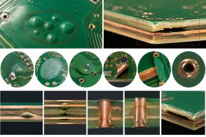
  • Inconsistent product quality: Many China PCB and assembly manufacturer cut corners on raw materials or process control, leading to PCB failures (e.g., copper foil peeling, impedance mismatch) that affect end-product performance.
  • Unreliable delivery times: Delays due to poor supply chain management or inefficient production processes disrupt clients’ project timelines and increase costs.
  • Lack of one-stop service: Needing to cooperate with multiple vendors for PCB design, fabrication, component sourcing, and assembly creates communication gaps and process inefficiencies.
  • Inability to handle complex requirements: Most PCB and assembly manufacturer in China fail to meet the strict technical standards for high-precision PCBs (e.g., HDI, extra thin PCB) used in medical, aerospace, and industrial equipment.
  • No transparent production traceability: Without a professional tracking system, clients cannot monitor production progress or verify process compliance, leading to quality risks.
  • Poor technical support: Lack of professional engineers to provide DFM (Design for Manufacturability) analysis results in design flaws that cause production delays and cost overruns.
  • Inability to meet industry-specific certifications: Many suppliers lack the necessary certifications for medical, aerospace, or automotive PCB manufacturing, making their products unqualified for these sectors.

Turnkey Solutions for PCB Manufacturing and Assembly We Offer

When navigating PCB manufacturing and assembly China, you need a strategic partner who understands your challenges and delivers tangible results. As a leading China PCB and assembly manufacturer, EBest’s turnkey one-stop services eliminate inefficiencies common with ordinary China PCB assembly and manufacturing suppliers, delivering cost savings and faster time-to-market while maintaining top quality.

To solve the pain point of fragmented vendor coordination, our integrated turnkey solution covers the entire PCB lifecycle. Key solutions include: end-to-end service from design optimization to final assembly and testing, PCB manufacturing and assembly China consolidating all your needs under one roof, and eliminating communication gaps and wasted time from juggling multiple vendors. This streamlines your process, cuts extra costs and delays, letting you focus on product innovation and business growth.

To fix inconsistent product quality, we implement a rigorous quality assurance system. Our specific solutions: use only high-grade certified raw materials from trusted global suppliers, conduct full-process inspections at every production stage, and deploy advanced testing equipment operated by seasoned engineers. These steps ensure your PCBs meet strict specifications for medical, aerospace or industrial use, with no costly reworks.

For reliable delivery, we’ve built a robust system to avoid project delays. Our solutions include: optimize supply chain management with long-term partnerships with trusted material suppliers, real-time production tracking via our advanced MES system, 24-hour urgent prototyping service for tight deadlines, and flexible scheduling to accommodate both small-batch prototypes and large-scale production.

To enhance your overall PCB manufacturing and assembly China experience, we add value with key support services: free DFM (Design for Manufacturability) analysis to optimize your designs before production, full production traceability to verify compliance at every step, and 24/7 multilingual technical support from our professional engineering team.

Why Choose EBest for China PCB Manufacturing and Assembly Factory?

Our advantages are tailored to your needs, focusing on efficiency, quality, and cost-saving, making us the top PCB fabrication and assembly manufacturer in China:

  • One-stop service: Save time and cut communication costs by letting us handle every stage of your PCB manufacturing and assembly China project from PCB design, prototyping, and fabrication to component sourcing, assembly, and testing. You’ll avoid the hassle of coordinating multiple vendors and reduce the risk of delays or miscommunication.​
  • Free DFM analysis: Protect your budget and keep projects on track with free DFM (Design for Manufacturability) analysis from our professional engineers. We identify design flaws early and optimize for manufacturability, eliminating costly rework, production delays, and wasted resources.​
  • MES system traceability: Gain full peace of mind with our advanced MES system, which tracks every production step from raw material input to final delivery. This transparency lets you monitor progress in real time, verify process compliance, and mitigate quality risks for your PCB manufacturing and assembly China orders.​
  • 24-hour urgent prototyping: Keep your project timeline on track even with tight deadlines. Our expedited 24-hour prototyping service ensures your PCB prototypes are shipped within a day, so you can accelerate product development and get to market faster.​
  • Small-batch customization: No MOQ (minimum order quantity) requirement means you can order as few as 1 piece—perfect for startups, R&D projects, or small-scale trials. This flexibility reduces your initial investment and lets you test ideas without unnecessary costs.​
  • 20+ years of expertise: Benefit from our deep industry knowledge, gained from serving global clients since 2006. We understand the unique PCB manufacturing and assembly requirements of medical, aerospace, and industrial equipment sectors, ensuring your PCBs meet strict industry standards.​
  • Multilingual technical support: Get fast, efficient solutions to your technical questions with 24/7 multilingual support from our professional engineers. No more language barriers or long wait times, we’re here to keep your projects moving smoothly.
Why Choose EBest for China PCB Manufacturing and Assembly Factory, https://www.bestpcbs.com/blog/2026/03/pcb-manufacturing-and-assembly-china/

What Types of China PCB Manufacturing and Assembly Services Can We Provide?

As a reliable China PCB manufacturing and assembly manufacturer, we offer a full range of services to meet diverse industry needs, including:

  • PCB Design: Custom design services tailored to your product requirements, including schematic design, PCB layout, and DFM optimization.
  • PCB Prototype: Rapid prototyping for all PCB types, with 24-hour urgent service and strict quality testing to ensure prototype accuracy.
  • Mass Production: Large-scale production with stable quality and high efficiency, supporting monthly output of 260,000 square feet.
  • Component Sourcing: Reliable component sourcing from certified suppliers, ensuring genuine parts and stable supply.
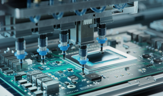
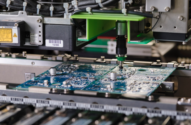
  • PCB Assembly: SMT (Surface Mount Technology) and through-hole assembly, with precision placement and soldering to meet industry standards.
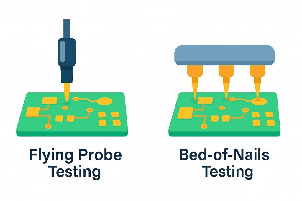
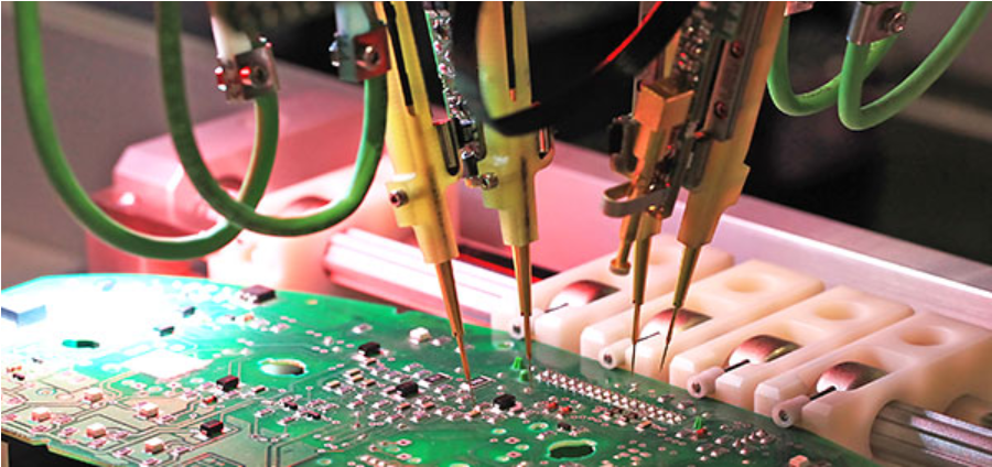
  • Testing Services: Comprehensive testing, including flying probe testing, functional testing, impedance testing, and thermal testing, to ensure PCB performance.
  • Custom PCB Fabrication: Specialized fabrication for various PCB types, including HDI, heavy copper, high-frequency, ceramic, and rigid-flex PCBs.

What Quality Certifications Has EBest Obtained for China PCB Manufacturing and Assembly?

Below are quality certifications for China PCB manufacturing and assembly orders we have:

  • IATF 16949: For automotive PCB manufacturing, ensuring compliance with automotive industry quality standards.
  • ISO 9001:2015: General quality management system certification, ensuring consistent product quality and service.
  • ISO 13485:2016: For medical PCB manufacturing, meeting the strict quality requirements of the medical device industry.
  • AS9100D: For aerospace PCB manufacturing, complying with aerospace industry standards for reliability and safety.
  • REACH: Compliance with EU regulations on chemical substances, ensuring our PCBs are safe for global markets.
  • RoHS: Compliance with EU RoHS directives, restricting hazardous substances in electronic products.
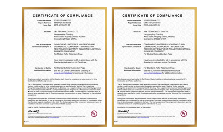
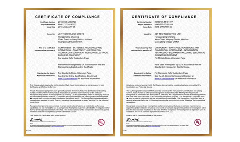
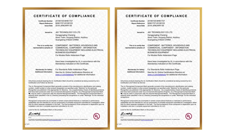
  • UL: Safety certification for electronic components, ensuring our PCBs meet global safety standards.

Our Quality Inspection Processes for China PCB Manufacturing and Assembly Orders

Incoming Material Inspection (IQC – Incoming Quality Control)

  • All raw materials (copper clad laminates, solder masks, solder pastes, components) undergo rigorous testing against international standards (e.g., IPC-4101 for laminates, J-STD-006 for solder).
  • Certificates of compliance (CoC) and material safety data sheets (MSDS) are verified.
  • Critical parameters like thickness, dielectric constant, and thermal conductivity are measured using precision instruments.

In-Process Inspection (IPQC – In-Process Quality Control)

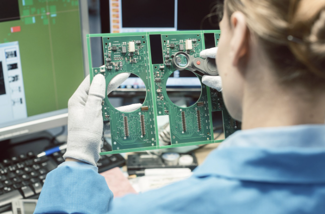
  • Automated Optical Inspection (AOI): Post-etching, post-solder mask, and post-soldering stages are inspected for defects (e.g., shorts, opens, misalignment).
  • X-ray Inspection: For BGA/QFN components to verify solder joint integrity and void analysis.
  • Flying Probe/ICT Testing: Electrical continuity and functionality checks during assembly.
  • Process Audits: Regular checks on operator adherence to SOPs (Standard Operating Procedures) and process parameters (e.g., temperature, pressure).

Final Quality Control (FQC)

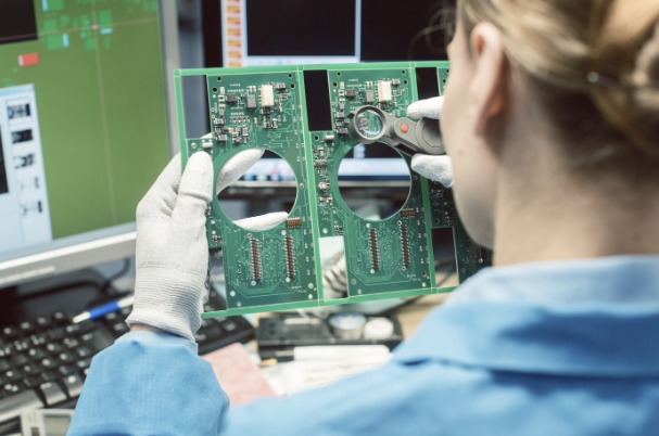
  • Visual Inspection: 100% board-level inspection for cosmetic defects (e.g., scratches, delamination) per IPC-A-600 standards.
  • Functional Testing: Full electrical testing (e.g., voltage, current, signal integrity) using automated test equipment (ATE).
  • Burn-In Testing: Accelerated life testing to identify early-life failures (e.g., thermal cycling, power cycling).

Reliability and Environmental Testing

  • Thermal Shock/Cycle Testing: -40°C to +125°C cycles to simulate extreme temperature changes.
  • Vibration/Shock Testing: Compliance with IEC 60068-2-6 (vibration) and IEC 60068-2-27 (shock).
  • Humidity/Salt Spray Testing: For corrosion resistance (e.g., 85°C/85% RH for 168 hours, salt spray per ASTM B117).

Packaging and Shipping Inspection

  • ESD-Safe Packaging: Anti-static bags, moisture barrier bags (MBBs), and desiccants to prevent electrostatic discharge (ESD) and humidity damage.
  • Labeling Compliance: RoHS/REACH compliance labels, part numbers, batch codes, and country-of-origin marking.
  • Shipping Audits: Random checks for packaging integrity and documentation (e.g., packing lists, certificates of conformance).

Documentation and Traceability

  • Batch Records: Detailed logs of material lots, machine settings, operator IDs, and test results.
  • Traceability Systems: Serialization and QR codes for end-to-end traceability from raw materials to finished goods.
  • Certificates of Analysis (CoA): Issued for each shipment, detailing test results and compliance with customer specifications.

Continuous Improvement and Customer Collaboration

  • Statistical Process Control (SPC): Real-time monitoring of critical process parameters (e.g., Cp/Cpk for capability analysis).
  • 8D/Corrective Action Reports (CAR): Root cause analysis for defects and preventive measures.
  • Customer Audits: Open access for customer quality audits and joint process improvement initiatives.
Our Quality Inspection Processes for China PCB Manufacturing and Assembly Orders, https://www.bestpcbs.com/blog/2026/03/pcb-manufacturing-and-assembly-china/

How Do We Ensure On-Time Delivery of PCB Manufacturing and Assembly Orders in China?

On-time delivery is critical for your project success, and EBest has established a robust system to ensure 97% on-time delivery rate for PCB manufacturing and assembly China orders:

  • Advanced Production Scheduling: We leverage intelligent scheduling software to optimize every production plan. This ensures we use our equipment and personnel efficiently, eliminating bottlenecks and keeping your PCB manufacturing and assembly China order on track from start to finish.
  • Robust Supply Chain Management: We’ve built long-term partnerships with reliable raw material and component suppliers. This stable supply network prevents delays caused by material shortages, ensuring your PCB production never gets held up.
  • MES System Real-Time Tracking: Our advanced MES system lets us monitor your order’s production progress in real time. We can spot potential delays early and take prompt corrective actions, keeping you informed and your project on schedule.
  • 24/7 Production Capacity: Our facilities operate around the clock, 24 hours a day, 7 days a week. This allows us to handle urgent orders efficiently and meet even the tightest deadlines for your PCB manufacturing and assembly China needs.
  • Flexible Production Lines: We have dedicated production lines for small-batch, large-scale, and urgent orders. This separation ensures each order is processed efficiently, with no interference, and delivered on time, regardless of size or urgency.
How Do We Ensure On-Time Delivery of PCB Manufacturing and Assembly Orders in China, https://www.bestpcbs.com/blog/2026/03/pcb-manufacturing-and-assembly-china/

Case Study: Medical PCB Production and Assembly for Cardiac Monitoring Device

Project Background

A leading European medical device manufacturer required high-precision PCBs for a next-generation cardiac monitoring system. The device needed to operate in extreme conditions (-40°C to +85°C) while maintaining 99.9% signal integrity over a 10-year lifecycle. The client chose our China-based facility due to our ISO 13485 certification, IPC Class 3 compliance, and proven track record in medical electronics.

Project Requirements

  • Technical Specifications: 12-layer HDI PCB with 0.08mm line/space, blind/buried vias, and ENIG surface finish.
  • Reliability Standards: Pass IEC 60601-1 (medical electrical equipment safety), MIL-STD-883 (thermal cycling), and ASTM F1979 (thermal shock).
  • Performance Metrics: â‰€0.1dB signal loss across 1-10GHz bandwidth, ≀1ÎŒV noise floor, and 100% electrical continuity.

Project Challenges

  • Microvia Reliability: 0.08mm laser-drilled microvias required <1% voiding in solder joints (measured via X-ray inspection).
  • Thermal Management: High-power components demanded thermal conductivity ≄3.0 W/mK in substrate materials.
  • ESD Sensitivity: Medical-grade components required <100V ESD protection during assembly.

Our Solutions

Material Selection: Rogers 4350B laminates with optimized dielectric constant (Dk=3.48±0.03) and low loss tangent (Df=0.0037).

Process Innovation:

  • AOI systems with 5ÎŒm resolution for post-etching defect detection (reduced false rejects by 15%).
  • X-ray inspection with 3D CT scanning for BGA solder joint analysis (achieved 99.8% voiding compliance).
  • Vacuum reflow ovens with O2 <100ppm for void-free soldering.

Reliability Testing:

  • 1,000 thermal cycles (-55°C to +125°C) with <5% resistance change.
  • 48-hour salt spray testing (ASTM B117) with zero corrosion.

Project Outcomes

  • Quality Metrics: 99.7% first-pass yield (up from client’s previous 92% supplier average).
  • Cost Efficiency: 25% cost reduction through optimized material usage and automated testing.
  • Delivery Performance: 14-day lead time (vs. industry average of 21 days) with 100% on-time delivery.

FAQs About PCB Manufacturing and Assembly China

Q1: What is the minimum order quantity (MOQ) for your PCB manufacturing and assembly China services?
A1: We have no MOQ requirement. We support small-batch orders (even 1 piece) for prototypes and R&D projects, as well as large-scale mass production. This flexibility helps startups and small businesses reduce initial costs, while meeting the needs of large enterprises for scalable production.

Q2: How long does it take to get a prototype for PCB manufacturing and assembly China?
A2: We offer 24-hour urgent prototyping service for simple PCBs (1-2 layers, FR4). For complex PCBs (multi-layer, HDI, high-frequency), the prototype lead time is 3-5 days. We prioritize urgent orders to ensure your project stays on track.

Q3: Can you handle custom PCB designs for medical and aerospace industries?
A3: Yes. We have rich experience in custom PCB design and manufacturing for medical, aerospace, and industrial equipment industries. Our team of professional engineers can optimize your design for manufacturability, and we hold ISO 13485, AS9100D, and IATF 16949 certifications to meet industry-specific requirements.

Q4: How do you ensure the quality of PCB manufacturing and assembly China orders?
A4: We implement a strict quality control process covering raw material inspection, in-process inspection, post-assembly testing, and final quality audit. We use advanced testing equipment and hold multiple quality certifications to ensure every PCB meets your specifications and global standards. Our MES system also provides full production traceability for transparency.

Q5: Do you provide DFM analysis for PCB manufacturing and assembly China?
A5: Yes, we provide free DFM analysis for all orders. Our engineers will review your PCB design to identify potential flaws (e.g., incorrect hole size, impedance mismatch) and optimize it for manufacturability, reducing rework, delays, and costs.

How to Get a Quote for China PCB Assembly and Manufacturing Service?

Ready to kickstart your pcb manufacturing and assembly china project with a fair, accurate quote—one that saves you time, cuts costs, and aligns perfectly with your goals? Don’t wait to move your project forward, please send your requirements to our dedicated sales team today via email: sales@bestpcbs.com — Your first step toward a seamless, high-quality PCB manufacturing experience.

To get a tailored quote fast (and avoid costly guesswork), include these key details: PCB design files (Gerber, PCB file), PCB type (FR4, HDI, ceramic, etc.), layer count, copper thickness, surface finish, order quantity, and any special requirements (certifications, lead time, etc.). Our expert team will respond within 24 hours with a detailed, transparent solution, plus free technical support to help you optimize your project and maximize value. Let’s turn your PCB vision into reality, together.

You may also like

Reliable PCB Assembly Ireland | High Quality & EU-Compliant

March 3rd, 2026

If you’re searching for reliable PCB assembly Ireland, EBest is your go-to partner, we specialize in high-precision, compliant PCB assembly in Ireland for medical, aerospace, and industrial sectors, and as a leading provider among PCB assembly companies in Ireland, we leverage 19+ years of industry experience and advanced technology to fulfill your unique project requirements, whether you need prototype development or large-scale mass production, with our PCB assembly in Ireland services delivering consistent quality, reliability, and on-time delivery every single time.

Common Pain Points in PCB Assembly Ireland

  • Component Shortages & Supply Chain Instability​: Many clients struggle with hard-to-find components and unstable supply chains.
  • Non-Compliance with EU Environmental Standards​: Ireland, as an EU member, enforces strict RoHS and REACH standards for electronic products.
  • Urgent Orders & Tight Delivery Timelines​: Users often need urgent PCB assembly in Ireland but struggle to find suppliers with quick turnaround.
  • Quality Issues & High Rework Rates​: Poor assembly quality leads to high rework costs and project delays.

Our Solutions to Pain Points of PCB Assembly Ireland

  • Tackling Component Shortages & Supply Chain Instability: We partner with top global component suppliers through long-term agreements to maintain a 15-day core material turnover rate. For critical components, we secure 3-5 certified backup suppliers and use dual-source procurement to avoid delays. Full supply chain transparency is ensured with blockchain tracking, so you always know where materials come from.
  • Meeting EU Environmental Compliance (RoHS & REACH): Our dedicated compliance team tracks EU standards like RoHS 3.0 and REACH SVHC updates in real time. All materials: solder, substrates, coatings are lead-free and halogen-free. Every batch is tested with XRF spectrometers for heavy metals and comes with third-party certifications like CE-RED and WEEE, guaranteeing 100% EU compliance.
  • Handling Urgent Orders & Tight Deadlines: Our SMT lines use dual-track high-speed placement machines paired with automated material handling to deliver prototypes in 48 hours and bulk orders in 72 hours. A 24/7 response team handles new product introductions with parallel engineering, simultaneously validating design, checking materials, and planning processes, cutting total lead time by 30%.
  • Reducing Quality Issues & Rework Costs: We follow Six Sigma quality control with visual inspection at key stages (placement, reflow, testing) to catch defects like misalignment or cold solder. Real-time monitoring of furnace temperatures and solder paste thickness ensures consistency. All technicians hold IPC-A-610 certification and undergo regular training, keeping first-pass yields above 99.5% and rework below 0.3%.

Why EBest Stands Out for PCB Assembly Ireland?

Reasons why choose EBest for PCB assembly in Ireland:

  • We offer 19+ years of one-stop expertise for Ireland PCB assembly, saving your engineering team time by eliminating the need to coordinate multiple suppliers from design to final assembly and avoiding costly trial-and-error with proven industry experience.​
  • Our monthly production capacity of 260,000 square feet (28,900 square meters) and ability to handle over 1,000 different boards ensures your projects, whether prototype or mass production, never face delays, accelerating your product launch timeline.​
  • We maintain full EU RoHS and REACH compliance to protect your engineering team from costly non-compliance penalties, shipment delays and product returns, letting you focus on innovation instead of regulatory headaches.​
  • Our comprehensive certifications (IATF 16949, ISO 9001:2015, ISO 13485:2016, AS9100D, UL) guarantee assemblies meet the strict quality standards required for medical, aerospace, and industrial applications, reducing rework and validation time.​
  • A stable component supply chain eliminates the frustration of component shortages and supply chain delays that derail your engineering projects, ensuring consistent access to all critical components (SMD, BGA, QFN, QFP).​
  • Our 24-hour expedite service for urgent orders keeps your engineering timeline on track even when deadlines tighten, avoiding costly project delays and helping you meet critical product launch or prototype testing milestones.​
  • Customizable solutions (flexible, ceramic, BGA, through-hole, full turnkey) tailor assemblies to your exact engineering specifications, no matter how complex, so your designs translate seamlessly into high-performance, reliable PCBs.​
  • Our dedicated engineering support team provides personalized assistance with design optimization, component selection and troubleshooting, reducing your team’s workload and ensuring your projects run smoothly from start to finish.​
  • We integrate certified processes and efficient supply chain management to deliver consistent, high-quality results for PCB assembly in Ireland, supporting your engineering team in meeting project goals on time and within standards.
Why EBest Stands Out for PCB Assembly Ireland, https://www.bestpcbs.com/blog/2026/03/reliable-pcb-assembly-ireland/

What PCB Assembly Services in Ireland Does EBest Offer?

Core PCB Assembly Services:

  • BGA Assembly Service: High-precision assembly for complex BGA components, ideal for advanced electronic devices.
  • Through-Hole Assembly: Reliable assembly for through-hole components, suitable for industrial equipment.
  • Flex PCB Assembly: Flexible PCB assembly for compact, lightweight devices in medical and aerospace industries.
  • Ceramic PCB Assembly: High-temperature resistant ceramic PCB assembly for extreme environment applications.

Value-Added Services:

  • PCB Fabrication: Prototypes and low-volume production with custom substrates or materials.
  • Injection Molding: Mold structure, thread insert, pad printing, laser engraving, and final assembly.
  • CNC Machining: CNC milling and turning with tight tolerances and anodizing options.
  • Sheet Metal: Low material waste, flexible material selection, and multiple finishing options.

What Quality Certifications Support EBest’s PCB Assembly in Ireland?

Below are quality certifications support EBest’s PCB assembly Ireland:

  • IATF 16949: Ensures quality for automotive-related PCB assembly in Ireland.
  • ISO 9001:2015: Guarantees consistent quality management for all PCB assembly services.
  • ISO 13485:2016: Complies with medical device standards for PCB assembly in Ireland.
  • AS9100D: Meets aerospace industry requirements for high-reliability PCB assembly.
  • RoHS / REACH / UL: Ensures EU environmental compliance and product safety.
What Quality Certifications Support EBest's PCB Assembly in Ireland, https://www.bestpcbs.com/blog/2026/03/reliable-pcb-assembly-ireland/

What Inspection Processes Does EBest Use for PCB Assembly Ireland?

Our EBest inspection process for PCB assembly Ireland:

  • Incoming Material Verification: Every component and raw material undergoes strict incoming inspection. We use XRF spectrometers to verify lead-free/halogen-free compliance (RoHS/REACH) and optical microscopy to check for physical defects like cracks or corrosion. Batch-specific certificates (e.g., CE-RED, WEEE) are cross-checked for traceability.
  • Automated Visual Inspection (AVI) at Key Production Stages: During SMT (Surface Mount Technology) placement, reflow soldering, and through-hole assembly, automated cameras scan for defects like misaligned components, solder bridges, or insufficient solder. This reduces human error and catches issues in real time.
  • Real-Time Process Monitoring with SPC: Statistical Process Control (SPC) software tracks critical parameters like oven temperature profiles, solder paste thickness, and placement pressure. Alerts trigger instantly if parameters drift outside tolerance, ensuring consistent quality and minimizing rework.
  • Functional Testing & First-Article Validation: Before bulk production, a “first article” PCB undergoes rigorous electrical testing (e.g., in-circuit tests, flying probe tests) to validate circuit functionality. For urgent orders, this step runs parallel with material checks and process planning to shorten lead times without compromising quality.
  • Final Quality Audit & Documentation: Every finished PCB batch passes a final audit where trained technicians (all IPC-A-610 certified) manually inspect for cosmetic defects, label accuracy, and packaging integrity. Detailed reports, including defect rates and corrective actions, are shared with clients for transparency.
  • Continuous Improvement via Six Sigma: Root-cause analysis is conducted for any defects found, using Six Sigma methodologies to prevent recurrence. Regular audits of processes and supplier performance ensure long-term quality stability.

Our PCB Assembly Capabilities for Ireland PCBA Orders

ItemCapabilities
Placer Speed13,200,000 chips/day
Bare Board Size0.2 x 0.2 inches – 20 x 20 inches/ 22*47.5 inches
Minimum SMD Component01005
Minimum BGA Pitch0.25mm
Maximum Components50*150mm
Assembly TypeSMT, THT, Mixed assembly
Component PackageReels, Cut Tape, Tube, Tray, Loose Parts
Lead Time1 – 5 days

Case Study: Large-Scale PCBA Assembly for Irish Continuous Glucose Monitoring Manufacturer

Project Background

We collaborated with an Irish medical technology firm specializing in CGM systems, a critical device for diabetes management that requires 24/7 reliable performance. The client needed a partner to support large-scale PCBA production for their next-generation CGM sensors, as their existing supplier could not meet the demand for 50,000 units per month while maintaining medical-grade quality.

The client faced challenges with scalability, inconsistent component sourcing, and strict traceability requirements, key priorities for medical devices that require 10-year process documentation per industry standards. They sought our expertise to build an automated, compliant production line for high-volume CGM PCBA assembly.

Project Requirements

  • ISO 13485:2016 compliant, with RoHS/REACH verification and 10-year full traceability for all components and assembly processes.
  • High-volume production of 50,000 PCBs monthly (100mm×60mm flex PCBs), with a 99.98% defect-free rate to meet scale and quality demands.
  • Assembly of ultra-fine pitch (0.4mm) BGA and SMD components, with placement accuracy of ±0.02mm to support the CGM’s high-sensitivity glucose sensing technology.
  • Automated production line integration to reduce human error and ensure consistent quality across high-volume batches.
  • Monthly delivery deadlines with zero delays, to support the client’s global distribution schedule for CGM systems.

Project Challenges

  • Scalability: Transitioning from small-batch to high-volume production without compromising quality or increasing rework rates.
  • Component Consistency: Sourcing large volumes of medical-grade components (including custom 0201-sized resistors) with consistent quality and on-time delivery.
  • Traceability: Maintaining 10-year documentation for 50,000 units monthly, requiring a digital tracking system to avoid gaps in component and assembly records.
  • Automation Integration: Aligning SMT chip, PCBA assembly, and testing processes into a seamless automated line to meet volume demands while adhering to medical standards.

Our Solutions

  • Scalable Production: We dedicated a fully automated production line to the project, with 4 SMT machines and 2 automated inspection stations, capable of handling 50,000+ PCBs monthly while maintaining precision.
  • Component Sourcing: We established a dedicated supply chain for high-volume medical-grade components, partnering with 3 EU-based suppliers to ensure consistent stock and pre-shipment testing for each batch.
  • Traceability System: We implemented a digital barcoding system for each component, PCB, and assembly step, storing data in a secure cloud platform to enable 10-year traceability and easy regulatory reporting.
  • Automated Quality Control: We integrated AOI optical scanning, X-ray inspection, and functional testing into the production line, with real-time process control to identify and resolve defects before they impact batch quality.

Project Results

  • Scalability: Successfully delivered 50,000 PCBs monthly, with a 99.99% defect-free rate, exceeding the client’s 99.98% requirement and reducing rework costs by 75% compared to their previous supplier.
  • Compliance: All PCBs passed third-party ISO 13485:2016 and RoHS/REACH verification, with 10-year traceability documentation fully compliant with Irish medical device regulations.
  • Timeline: Met 12 consecutive monthly delivery deadlines with zero delays, supporting the client’s global CGM distribution and increasing their market share by 15%.
  • Efficiency: The automated production line reduced production time by 40% compared to the client’s previous process, lowering per-unit costs while maintaining medical-grade quality.
Large-Scale PCBA Assembly for Irish Continuous Glucose Monitoring Manufacturer, https://www.bestpcbs.com/blog/2026/03/reliable-pcb-assembly-ireland/

FAQs About PCB Assembly in Ireland

Q1: How long does PCB assembly in Ireland take at EBest?
A1: Our PCB assembly timelines are optimized for efficiency without compromising quality. Standard orders are completed in 3-5 business days while urgent orders can be shipped within 24 hours thanks to our flexible production lines and dedicated resources for time-sensitive projects. The exact timeline is tailored to your order volume and complexity, ensuring on-time delivery to keep your engineering projects on track.

Q2: Does EBest provide custom PCB assembly in Ireland?
A2: Yes, we specialize in fully customizable PCB assembly solutions to match your exact engineering specifications. Our custom services include a wide range of options from custom substrates and materials to specialized assembly techniques such as BGA, flexible and ceramic PCB assembly. This flexibility ensures your unique design requirements are met seamlessly, translating your ideas into high-performance reliable PCBs.

Q3: Is EBest’s PCB assembly in Ireland compliant with EU standards?
A3: Absolutely. All our PCB assembly in Ireland is fully compliant with EU RoHS and REACH standards, backed by industry-leading certifications and third-party verification. Our strict compliance processes and use of lead-free EU-approved materials eliminate the risk of shipment delays, penalties and non-compliance issues, letting you focus on innovation instead of regulatory headaches.

Q4: Can EBest handle small-batch prototype PCB assembly in Ireland?
A4: Yes, we excel at small-batch prototype PCB assembly with flexible production lines designed to handle these orders efficiently and cost-effectively. Our 19+ years of expertise ensures prototypes are built with the same precision and quality as mass production runs, accelerating your product launch timeline and reducing costly trial-and-error.

Q5: Does EBest offer component sourcing for PCB assembly in Ireland?
A5: Yes, we provide end-to-end component sourcing through our resilient multi-layered global supply network. Our dedicated purchasing team leverages years of industry experience to secure all electronic components including SMD, BGA, QFN and QFP, with strategic inventory for high-demand parts. This eliminates the need for you to source materials separately, saving your engineering team time and avoiding project delays from component shortages.

You may also like

Premium PCB Assembly in Japan | One-Stop PCBA Solutions

March 2nd, 2026

When looking for a reliable PCB assembly manufacturer in Japan, EBest is your top choice for professional, efficient, and high-quality solutions. PCB assembly in Japan requires strict precision and compliance with international standards, which EBest has mastered after 19 years of industry experience. We focus on delivering top-tier PCB assembly in Japan, catering to diverse industry needs with customized services. Many PCB assembly companies in Japan prioritize quality and speed, and EBest stands out by integrating one-stop solutions to meet every client’s unique requirements.

PCB assembly in Japan, https://www.bestpcbs.com/blog/2026/03/pcb-assembly-in-japan/

Common Pain Points of PCB Assembly in Japan

  • Unstable Component Supply: A major pain point in PCB assembly in Japan, often caused by tight supply of high-end materials and fluctuating market demand. EBest solves this with a robust, stable supply chain covering all electronic components (SMD, BGA, QFN, QFP), ensuring steady access to genuine, high-quality parts even amid industry supply shortages.​
  • Strict Quality Compliance Requirements: Clients face challenges meeting Japan’s rigorous industry standards and METI certification demands for PCB assembly in Japan. EBest eliminates compliance risks by adhering to all local and international certifications, including ISO 9001, ISO 13485, and AS9100D.​
  • Tight Delivery Timelines: Urgent projects often struggle with delayed turnarounds in PCB assembly in Japan. Our 24-hour expedite service ensures fast, reliable delivery, even for critical orders, without compromising quality.​
  • Complex High-Precision Assembly Needs: AI-driven and high-end devices require micron-level precision for PCB assembly in Japan. EBest’s advanced R&D and automated assembly lines handle complex components (e.g., BGA) with exceptional accuracy.​
  • Lack of Tailored Solutions: Many PCB assembly companies in Japan offer one-size-fits-all services. EBest provides customized solutions to match the unique needs of medical, aerospace, and industrial equipment industries.​
  • Compliance Documentation Burdens: Clients often struggle with preparing and maintaining METI-compliant documentation for PCB assembly in Japan. EBest offers end-to-end support for document preparation, ensuring full compliance with local regulations.

Our Solutions to These Pain Points of Japan PCB Assembly

  • Build a global dual-supply chain system, cooperating with 12+ certified component suppliers (covering SMD, BGA, QFN, QFP) to lock high-end materials in advance. Prepare 5%-8% spare parts for core components to avoid delays caused by market supply fluctuations, ensuring 100% on-time component delivery.​
  • Equip a dedicated compliance team, fully aligning with METI standards and international certifications (ISO 9001, ISO 13485, AS9100D). Implement pre-production compliance review and post-production certification verification to eliminate all compliance risks for clients.​
  • Allocate dedicated automated production lines for urgent orders, adopt intelligent scheduling via MES system to shorten production cycle by 15%. Launch 24-hour expedite service with 3-person dedicated follow-up, ensuring critical orders are delivered on time without quality compromise.​
  • Use advanced automated SMT assembly lines with ±0.03mm positioning accuracy, match professional X-ray detection equipment to inspect BGA and other complex components. Our R&D team optimizes soldering processes (±1℃ reflow soldering precision) to meet micron-level requirements of AI-driven and high-end devices.​
  • Assign industry-specific engineers (medical, aerospace, industrial control), conduct 1-on-1 demand communication to customize processes, materials and testing standards. Integrate one-stop service from design optimization to final assembly to fully match client-specific needs.​
  • Provide end-to-end METI-compliant documentation support, including document preparation, review and update. Our professional team ensures all documents meet relevant local regulations, saving clients time and energy in documentation management.

Why Choose EBest for PCB Assembly in Japan?

Reasons why choose EBest for PCB assembly in Japan:

  • Advanced MES System: We equip a professional MES system for PCB assembly in Japan, realizing full-process intelligent management and product traceability, which helps you track every production link, reduce quality risks, and ensure product consistency and traceability.
  • One-Stop PCBA Solutions Service: We provide full-turnkey one-stop PCB assembly services for clients in Japan, covering PCB production, component sourcing, SMT/DIP assembly, functional testing and final packaging, saving you time and costs of cooperating with multiple suppliers.​
  • Authoritative Quality Certifications: We hold AS9100D (aerospace industry), ISO 13485:2016 (medical industry), IATF 16949 (automotive industry) and ISO 9001:2015 certifications, ensuring our PCB assembly in Japan fully meets the strict quality requirements of various industries.​
  • Stable and Reliable Component Supply: We have a robust global supply chain, ensuring stable access to genuine, high-quality electronic components (SMD, BGA, QFN, QFP) for PCB assembly in Japan, avoiding project delays caused by component shortages .​
  • High Production Capacity & Efficiency: With a monthly production capacity of 260,000 square feet (28,900 square meters) and automated production lines, we can efficiently handle both high-volume and low-volume/prototype PCB assembly in Japan, shortening your delivery cycle.​
  • Industry-Specific Customization: We provide customized PCB assembly in Japan solutions for medical, aerospace, and industrial equipment industries, tailoring services to meet the unique technical and compliance needs of your industry.​
  • Strict Quality Control: We implement 100% full inspection before delivery, adopt A+ grade materials, and follow IPC-A-610J CLASS III acceptance standards, ensuring the pass rate of PCB assembly in Japan reaches 99% or above.​
  • Professional R&D Support: We invest heavily in R&D to keep pace with Japan’s electronic manufacturing trends, providing technical support for complex high-precision PCB assembly, helping you realize product innovation and upgrading.​
  • Comprehensive After-Sales Service: We offer professional after-sales support for PCB assembly in Japan, including technical consultation, troubleshooting and maintenance guidance, solving your worries after order delivery.
Why Choose EBest for PCB Assembly in Japan, https://www.bestpcbs.com/blog/2026/03/pcb-assembly-in-japan/

What Services Does EBest Offer for PCB Assembly in Japan?

Core PCB Assembly Services​:

  • BGA Assembly Service: High-precision PCB assembly for complex BGA components, tailored for advanced electronic devices in Japan. Our micron-level accuracy ensures stable performance, perfectly suited for AI-driven and high-tech products dominating Japan’s market.​
  • Through-Hole Assembly: Reliable through-hole component assembly for PCB assembly in Japan, delivering strong connectivity and long-term durability. Ideal for industrial equipment and rugged electronic devices requiring consistent performance in harsh environments.​
  • Flex PCB Assembly: Flexible PCB assembly solutions for compact, high-performance devices—perfect for Japan’s electronics industry, where miniaturization and portability are key demands for consumer and industrial products.​
  • Quick Turn PCB Assembly: Expedited PCB assembly in Japan for urgent orders, with 24-hour delivery for critical projects. Aligns with Japan’s fast-paced manufacturing cycle, supporting your “small-batch, quick-turn” production needs.​
  • Full Turnkey PCB Assembly: One-stop PCB assembly service for Japan’s clients, covering PCB production, component sourcing, SMT/DIP assembly, functional testing, and final packaging. Saves you time and costs by eliminating the need to coordinate multiple suppliers.​

Value-Added Services​:

  • Injection Molding: Comprehensive injection molding services to complement PCB assembly in Japan, including mold structure design, thread insert, pad printing, laser engraving, and final assembly, streamlining your production process.​
  • CNC Machining: High-precision CNC Milling and Turning with tight tolerances and anodizing options, designed to match the strict quality standards of PCB assembly in Japan for aerospace, medical, and industrial applications.​
  • Sheet Metal: Efficient sheet metal services for PCB assembly projects in Japan, featuring low material waste, flexible material selection, and multiple finishing options, reducing costs while ensuring compatibility with your PCB designs.

What Quality Certifications Does EBest Hold for PCB Assembly in Japan?

  • IATF 16949: This certification ensures our PCB assembly in Japan fully complies with the strict quality and safety requirements of the automotive industry, supporting your automotive electronic component assembly needs.​
  • ISO 9001:2015: As a globally recognized quality management standard, it guarantees consistent quality control across all our PCB assembly services, delivering reliable results for every client in Japan.​
  • ISO 13485:2016: Tailored for the medical device industry, this certification ensures our PCB assembly in Japan meets the rigorous standards for medical equipment, prioritizing safety and zero-fault performance.​
  • AS9100D: Compliant with aerospace industry requirements, this certification is critical for high-reliability PCB assembly, making us a trusted partner for aerospace component assembly in Japan.​
  • RoHS & REACH: These environmental certifications ensure our PCB assembly in Japan meets both local and global environmental standards, restricting harmful substances and aligning with international new pollutant control requirements.​
  • UL: This safety certification guarantees the compliance and safety of electronic components used in our PCB assembly in Japan, reducing safety risks for your end products.
What Quality Certifications Does EBest Hold for PCB Assembly in Japan, https://www.bestpcbs.com/blog/2026/03/pcb-assembly-in-japan/

Our PCB Assembly Capabilities for Japan PCBA Orders

ItemCapabilities
Placer Speed13,200,000 chips/day
Bare Board Size0.2 x 0.2 inches – 20 x 20 inches/ 22*47.5 inches
Minimum SMD Component01005
Minimum BGA Pitch0.25mm
Maximum Components50*150mm
Assembly TypeSMT, THT, Mixed assembly
Component PackageReels, Cut Tape, Tube, Tray, Loose Parts
Lead Time1 – 5 days

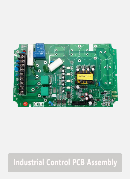
​Case Studies: Industrial Control PCB Prototyping in Japan

Custom Rigid-Flex PCB Assembly Project for Japanese Industrial Automation Client

Project Background: Our client is a leading Japanese industrial automation manufacturer specializing in smart factory control systems. Amid Japan’s booming industrial automation demand and equipment upgrades, their existing PCB assemblies had frequent signal interference, causing 8-10 monthly malfunctions, reducing production efficiency by 18% and increasing maintenance costs significantly.

Project Requirements:

  • Produce custom rigid-flex PCB assembly in Japan for control modules: 1.2mm thickness, 12 layers, 860+ components (SMD, BGA, through-hole).​
  • Withstand harsh industrial conditions: -40℃ to 85℃ operating temperature, 10-2000Hz vibration resistance, 95% humidity resistance (non-condensing).​
  • Comply with ISO 9001:2015, IATF 16949, and Japan’s METI industrial control standards.​
  • Deliver 5,000 units in 25 business days; prototype approval within 5 days.​
  • Guarantee ≄99.8% pass rate and ≄80,000-hour service life.​

Project Difficulties​:

  • High precision: 0.5mm pitch BGA components require ±0.03mm assembly accuracy; rigid-flex connection prone to poor soldering and signal loss.​
  • Environmental adaptability: Strict material/soldering requirements to resist temperature cycles and industrial vibration.​
  • Tight timeline: 25-day delivery for 5,000 units plus 5-day prototype approval requires efficient scheduling.​
  • Component supply: High-temperature resistant components were in tight supply amid Japan’s industrial equipment boom.​

Solutions​

  • Precision assembly: Used automated lines + MES system for full traceability; ±1℃ reflow soldering precision to ensure BGA soldering quality.​
  • Material optimization: Selected A+ grade FR-4+PI rigid-flex substrates and IPC-CC-830 conformal coating; 100+ environmental tests to verify performance.​
  • Efficient scheduling: Allocated dedicated lines (260,000 sq.ft/month capacity); 15% assembly time reduction via one-stop service.​
  • Stable supply: Locked 100% of required components in advance with 5% spares to avoid delays.​
  • Quality control: 100% AOI + X-ray inspection; 5% functional testing to ensure compliance.​

Output Results​

  • Delivery: 5,000 units delivered 2 days early (23 business days); prototype approved in 4 days.​
  • Quality: 99.92% pass rate, exceeding the 99.8% requirement; no signal interference or soldering defects.​
  • Performance: Client’s monthly malfunctions dropped to 0-1; production efficiency improved by 28%.​
  • Compliance: Passed METI inspection and ISO 9001/IATF 16949 audits.​
  • Longevity: 85,000-hour service life, exceeding the 80,000-hour requirement.
Case Studies: Industrial Control PCB Prototyping in Japan, https://www.bestpcbs.com/blog/2026/03/pcb-assembly-in-japan/

FAQs About PCB Assembly in Japan

Q1: How long does EBest take for PCB assembly in Japan?​
A1: Standard orders take 3-7 business days, while our quick turn service delivers urgent PCB assembly in Japan within 24 hours. Lead times are tailored to order volume and complexity.​

Q2: Does EBest provide component sourcing for PCB assembly in Japan?​
A2: Yes, we have a stable supply chain for all electronic components (SMD, BGA, QFN, QFP, etc.) for PCB assembly in Japan, ensuring genuine, high-quality parts with full traceability.​

Q3: Is EBest’s PCB assembly in Japan compliant with RoHS and REACH?​
A3: Absolutely. All our PCB assembly in Japan meets RoHS and REACH requirements, using lead-free materials and processes to ensure environmental compliance.​

Q4: Can EBest produce prototype PCB assembly in Japan?​
A4: Yes, we offer prototype PCB assembly in Japan for low-volume production, with customization options for special substrates or materials to support product development.​

Q5: How does EBest ensure quality for PCB assembly in Japan?​
A5: We implement 100% full inspection before delivery, use A+ grade materials, and follow strict quality control processes aligned with our ISO and industry-specific certifications.

You may also like

High Quality PCB Prototype Japan | No MOQ & Expedited Service

March 2nd, 2026

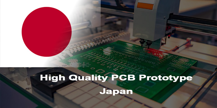
EBest Circuit provides high-quality PCB prototype Japan services with no MOQ requirement and expedited delivery, solving common production challenges for clients in Japan. Our PCB prototype Japan solutions are tailored to meet the strict standards of the Japanese electronics industry, combining 20 years of manufacturing experience with advanced technology to deliver reliable, fast, and cost-effective results.

High Quality PCB Prototype Japan, https://www.bestpcbs.com/blog/2026/03/pcb-prototype-japan/

Are You Struggling With These Common Pain Points of PCB Prototype Japan?

  • Do you face long lead times that delay your PCB prototype Japan development schedule?​
  • Is it difficult to find manufacturers that accept small orders for PCB prototype Japan without high minimum quantity requirements?​
  • Do you encounter quality issues such as signal interference or poor precision with your PCB prototype Japan?​
  • Are you unable to get free design feedback to optimize your PCB prototype Japan before production?​
  • Do you struggle with tracking production progress for your PCB prototype Japan orders?​
  • Is it challenging to find PCB prototype Japan manufacturers with recognized quality certifications?​
  • Do you face high costs when ordering small-batch PCB prototype Japan services?

Our Tailored Solutions for Japan PCB Prototype Challenges

  • To solve long lead time issues: We offer expedited service for PCB prototyping Japan, with urgent orders shipped within 24 hours, effectively shortening your product development cycle and ensuring timely progress.
  • To address small-batch order difficulties: We have no MOQ requirement, freely accepting small-batch orders to fully support your trial production and R&D needs without extra constraints.
  • To eliminate quality concerns: We use advanced production equipment and strict quality control protocols, effectively avoiding signal interference and ensuring high precision that meets Japan’s strict industry standards.
  • To reduce design-related errors: We provide free DFM (Design for Manufacturability) analysis, helping you optimize designs in advance and minimize production errors.
  • To solve progress tracking troubles: We adopt MES systems to track real-time production data, allowing you to monitor your order progress anytime, anywhere for full transparency.
  • To meet certification requirements: We hold ISO 9001:2015, ISO 13485:2016, and AS9100D certifications, ensuring every product meets international quality standards and complies with industry regulations.
  • To cut small-batch costs: We optimize production processes to reduce costs, offering competitive pricing for small-batch services, balancing quality and cost-effectiveness.

Why EBest Is Your Trusted Partner for PCB Prototype in Japan?

Reasons why EBest is your trusted partner for PCB prototype in Japan:

  • Expedited Service: Exclusive expedited channel, with PCB prototype Japan urgent orders shipped within 24 hours, far exceeding the industry average delivery speed, helping accelerate R&D progress and seize market opportunities.​
  • No MOQ Restriction: Completely break the barrier of small-batch orders, no minimum order quantity required, supporting orders starting from 1 piece, perfectly adapting to R&D trial production and small-batch customization needs, and reducing initial investment costs.​
  • Free DFM Analysis: Professional team provides free Design for Manufacturability (DFM) analysis, avoiding design defects in advance, reducing production rework, shortening the delivery cycle of PCB prototype Japan, and lowering R&D losses.​
  • 20 Years of Industry Experience: Deeply engaged in the PCB manufacturing industry for 20 years, gathering an elite team of the industry, familiar with Japanese electronic industry standards, with mature prototype production capabilities to ensure professional and reliable services.​
  • Authoritative Qualification Certifications: Hold international authoritative certifications such as ISO 9001, ISO 13485, and AS9100D, strictly following quality systems to ensure every batch of PCB prototype Japan complies with Japanese industry standards.​
  • Trackable Production Data: Equipped with a professional MES system to track real-time full-process production data, with transparent and checkable order progress, allowing you to grasp the production dynamics of PCB prototype Japan at any time without repeated inquiries.​
  • Customized Solutions: Provide flexible customization services according to different technical needs and application scenarios, covering various types of PCB prototype Japan to adapt to personalized needs of multiple industries.​
  • Exclusive After-Sales Support: Equipped with a professional service team to follow up one-on-one throughout the process, responding to inquiries in a timely manner and solving problems in the entire order process, making the purchase of PCB prototype Japan more worry-free and assured.
Why EBest Is Your Trusted Partner for PCB Prototype in Japan, https://www.bestpcbs.com/blog/2026/03/pcb-prototype-japan/

PCB Prototype Types We Provide for the Japanese Market

Below are PCB prototype types we provide for the Japanese market:

  • Flexible PCBs: Lightweight, bendable, and space-saving, ideal for compact electronic devices in Japan that require flexible installation.​
  • Rigid PCBs: Stable structure and high durability, suitable for most standard electronic applications, meeting Japan’s strict quality requirements for PCB prototype Japan.​
  • Rigid-Flex PCBs: Combine the advantages of rigid and flexible boards, perfect for complex device designs that need both stability and flexibility.​
  • Ceramic PCBs: Excellent high-temperature resistance and insulation performance, compatible with Japan’s advanced electronic component manufacturing, such as precision ceramic-based products.​
  • Metal Core PCBs (MCPCBs): Superior heat dissipation, ideal for high-power electronic devices common in the Japanese market.​
  • High-Frequency PCBs: Low signal loss, designed for communication and radar equipment, meeting Japan’s high standards for signal stability.​
  • FR4 PCBs: Cost-effective and versatile, the most widely used type for general PCB prototype Japan orders.​
  • HDI PCBs: High-density interconnection, supporting miniaturization, aligned with Japan’s focus on compact, high-performance electronic components.​
  • High TG PCBs: High glass transition temperature, resistant to high temperatures, suitable for harsh working environments.​
  • Heavy Copper PCBs: Thick copper layers for high-current applications, ensuring stable performance in industrial and automotive electronics.​
  • Impedance Control PCBs: Precise impedance control, critical for high-frequency devices, complying with Japan’s strict technical standards.

Strict Quality Standards for Japan PCB Prototype Manufacturing

  • Authoritative Quality System Compliance: All PCB prototype Japan production strictly follows ISO 9001:2015, ISO 13485:2016, and AS9100D quality management systems, ensuring consistent quality that meets international and Japanese industry requirements.​
  • Green Raw Material Selection: We use high-quality raw materials that fully comply with RoHS and REACH standards, restricting harmful substances and aligning with global green development trends and Japan’s environmental requirements.​
  • High-Precision Component Control: For high-precision PCB prototype Japan, we control the minimum SMD component size to 01005 and the minimum BGA pitch to 0.25mm, ensuring compatibility with Japan’s advanced compact electronic components.​
  • Strict Impedance Accuracy: For high-frequency PCB prototype Japan, we guarantee impedance control accuracy with a deviation of no more than ±10%, ensuring stable signal transmission for high-frequency devices.​
  • High Qualification Rate Guarantee: We maintain a product qualification rate of over 99.5% for all PCB prototype Japan orders, minimizing defects and reducing your rework and delay risks.​
  • Precise Dimensional Tolerance: We adhere to strict dimensional tolerance standards, ensuring every PCB prototype Japan perfectly matches your design specifications and fits seamlessly into your electronic devices.

Our Comprehensive Quality Control Process for PCB Prototypes

  • Raw material inspection: Test all substrates, copper foils, and components for PCB prototype Japan to ensure they meet quality standards.
  • Design review: Conduct free DFM analysis to check for design flaws that may affect PCB prototype Japan production.
  • In-process inspection: Monitor key production steps such as lamination, drilling, and etching for PCB prototype Japan to avoid defects.
  • Electrical testing: Use flying probe testing and AOI optical inspection to check for short circuits, open circuits, and other issues in PCB prototype Japan.
  • Final inspection: Conduct overall quality checks on dimensions, appearance, and performance of PCB prototype Japan before packaging.
  • Packaging inspection: Ensure PCB prototype Japan is packaged with anti-static materials to prevent damage during transportation.
Our Comprehensive Quality Control Process for PCB Prototypes, https://www.bestpcbs.com/blog/2026/03/pcb-prototype-japan/

Fast & Reliable Lead Time for PCB Prototypes in Japan

Our lead time for FR4 PCB prototyping:

LayersNormal ServiceFastest Service
17 Days24 H
28 Days24 H
410 Days48 H
610 Days72 H
812 Days72 H
≄10TBDTBD

Our lead time for MCPCB prototyping:

LayersNormal ServiceFastest Service
14 Days24 H
214 Days168 H
421 DaysTBD

Here are Lead time for other boards:

ItemsNormal ServiceFastest Service
FPC48-72 H24 H
Rigid- Flex2 Weeks for 4L1.5 Weeks for 4L
>4L: TBD>4L: TBD
Ceramic3 Weeks2 Weeks

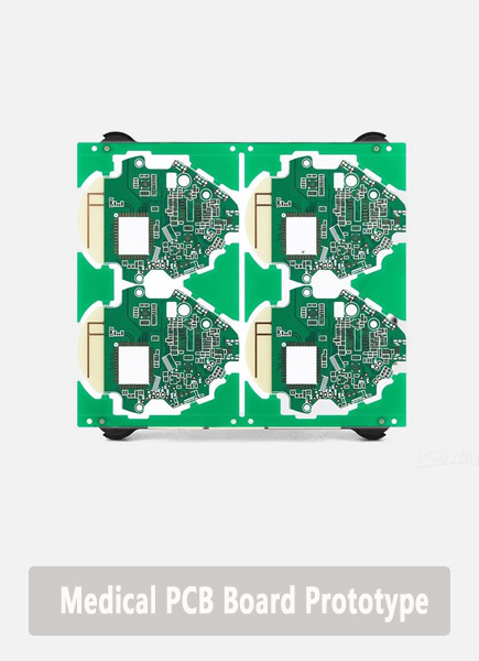
Case Studies: Medical PCB Prototyping in Japan

Project Background: A Japanese medical device firm needed a high-precision PCB prototype Japan for a portable diagnostic device. The project required strict compliance with medical industry standards, which align with global medical equipment safety requirements. Tight delivery timelines were also essential to support the client’s product launch schedule.​

Project Requirements: The specified PCB prototype Japan was a 6-layer HDI board. It required a 0.3mm BGA pitch, 50Ω impedance control, ISO 13485:2016 compliance, a 3-day lead time and a minimum 99% qualification rate. These requirements were non-negotiable for medical device applications, as precision and reliability are critical in medical equipment manufacturing.

​Project Challenges: The primary challenge was balancing three critical demands: 3-day expedited delivery, high precision with a 0.3mm BGA pitch and strict medical quality standards. The client also required real-time production progress tracking to ensure transparency and on-time delivery, a key concern for medical device R&D timelines.​

Our Solutions: We assigned a dedicated team to the PCB prototype Japan project to prioritize efficiency. We used high-precision production equipment to meet the 0.3mm BGA pitch requirement. We also leveraged our MES system for real-time progress updates and conducted pre-production DFM analysis to eliminate design flaws and prevent delays.​

Output Results: We delivered the PCB prototype Japan exactly within the 3-day deadline and achieved a 99.8% qualification rate that exceeded the client’s requirement. The client verified full compliance with medical standards and performance expectations. They praised our service as “reliable, fast, and professional” and signed a long-term cooperation agreement for future PCB prototype Japan orders.

Medical PCB Prototyping in Japan, https://www.bestpcbs.com/blog/2026/03/pcb-prototype-japan/

Frequently Asked Questions About PCB Prototyping in Japan

Q1: Can I order small-batch PCB prototype Japan without a minimum order quantity?
A1: Yes, we have no MOQ requirement for PCB prototyping Japan, accepting orders of any quantity to support your R&D and trial production needs.?

Q2: How fast can you deliver urgent PCB prototype in Japan orders?
A2: We provide expedited service for PCB prototype Japan, with urgent orders (single-sided, double-sided) shipped within 24 hours, and multi-layer prototypes shipped within 48-72 hours.?

Q3: Do you provide free design feedback for PCB prototyping Japan?
A3: Yes, we offer free DFM analysis for all PCB prototype Japan orders, helping you optimize designs to reduce production errors and costs.?

Q4: Are your PCB prototype in Japan products compliant with medical industry standards?
A4: Yes, we hold ISO 13485:2016 certification, and our PCB prototype Japan for medical devices meets strict medical quality and safety standards.?

Q5: Can I track the production progress of my PCB prototyping Japan order?
A5: Yes, we use MES systems to track real-time production data for PCB prototype Japan, allowing you to check order progress anytime through our service channel.

You may also like

What is a .BRD File in PCB Design?

March 2nd, 2026

A .brd file is a native PCB layout file used by electronic design automation (EDA) software to store the physical board design of a printed circuit board. Unlike schematic files that represent logical connections, a .brd file defines the actual board geometry, copper routing, layers, drill data, footprints, and manufacturing constraints required for fabrication and assembly.

In practical terms, when an engineer finishes routing traces, placing components, defining stack-up layers, and setting design rules, that layout data is saved as a .brd file. It is the working design file—not the final manufacturing output like Gerber files.

What Is a .brd File?

A .brd file is the board layout file generated by certain Electronic Design Automation (EDA) tools. It stores the complete PCB layout environment, including:

  • Board outline geometry
  • Copper trace routing
  • Via definitions
  • Layer stack configuration
  • Component footprints and placement
  • Design rules and constraints
  • Net connectivity

In simple terms:

  • A schematic file (.sch) defines logical connections.
  • A .brd file defines the physical realization of those connections.

The .brd file represents the stage where abstract circuitry becomes manufacturable hardware.

What is a .BRD File in PCB Design?

What Is the BRD File Format?

The BRD file format is proprietary and software-dependent. Different PCB tools use “.brd” as their internal layout database extension, but the internal structures are not interchangeable.

For example:

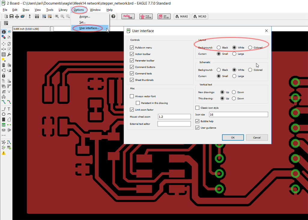
  • Autodesk EAGLE uses .brd to store board layout data.
  • Cadence Allegro also uses .brd as its main PCB database format.
  • Mentor Graphics PADS historically used similar board database structures.

Although the file extension is identical, the file encoding, object hierarchy, and internal database schema vary significantly.

This means:

  • An EAGLE .brd file cannot be directly opened in Allegro.
  • An Allegro .brd file cannot be imported natively into EAGLE.

Therefore, when someone shares a .brd file, always confirm:

  1. Which software created it
  2. Which software version was used

Even minor version mismatches can cause compatibility issues.

Information Contained in a .BRD File

A .brd file is essentially the master PCB database. It contains nearly everything required to reproduce the board layout in a design environment.

1. Board Mechanical Definition

The file includes:

  • Board outline dimensions
  • Cutouts and slots
  • Edge contours
  • Mounting hole locations
  • Keep-out regions

Mechanical integrity depends on these parameters. Incorrect outline data can lead to enclosure mismatch or assembly failure.

2. Layer Stack Definition

The layer stack is a critical element stored in the .brd file:

  • Number of layers (2L, 4L, 6L, 10L, etc.)
  • Signal layers
  • Power/ground planes
  • Dielectric spacing
  • Copper thickness

In advanced designs such as HDI or high-speed boards, stack-up configuration affects:

  • Impedance control
  • Crosstalk performance
  • EMI behavior
  • Thermal dissipation

The .brd file stores these definitions so the design rules can reference them dynamically.

3. Copper Routing and Nets

The routing database inside a .brd file contains:

  • Trace width
  • Trace length
  • Via types
  • Differential pair constraints
  • Length matching settings

In high-speed applications (DDR, PCIe, RF), this data is crucial. The .brd file tracks connectivity integrity in real time and allows DRC validation.

Information Contained in a .BRD File

4. Component Placement Data

The file records:

  • XY coordinates
  • Rotation angles
  • Layer (top/bottom)
  • Reference designators
  • Footprint library mapping

This placement information is later used to generate:

  • Pick-and-place files
  • Assembly drawings
  • 3D board models

Without accurate placement data in the .brd file, assembly automation would be impossible.

5. Drill and Via Database

The .brd file includes:

  • Through-hole vias
  • Blind vias
  • Buried vias
  • Microvias
  • Drill diameters
  • Backdrill definitions

These parameters determine:

  • Fabrication cost
  • Reliability
  • Yield rate
  • Manufacturability

Advanced HDI structures rely heavily on precise via definitions stored inside the board file.

6. Design Rule Constraints

One of the most powerful aspects of a .brd file is its embedded DRC rules, including:

  • Minimum trace width
  • Clearance rules
  • Solder mask expansion
  • Annular ring requirements
  • Impedance rules
  • High-voltage spacing

These constraints prevent layout errors and ensure compliance with fabrication capability.

What Opens a .BRD File?

A .brd file must be opened using the software that created it or a compatible tool.

Common tools include:

  • Autodesk EAGLE
  • Cadence Allegro
  • KiCad (import functionality available)
  • Altium Designer (via import wizard)

Before opening a .brd file:

  1. Verify software origin
  2. Confirm version compatibility
  3. Check library dependencies

Missing footprint libraries can cause loading errors.

How to View .BRD File?

If editing is not required, viewing options include:

Option 1: Install Viewer Mode

Some PCB tools provide free viewing licenses.

Option 2: Convert to Neutral Format

Export:

  • Gerber files
  • ODB++
  • IPC-2581

These can be viewed using standard PCB viewers.

Option 3: 3D Export

Many modern tools allow exporting a 3D STEP model for mechanical review.

In professional workflows, contract manufacturers rarely request the .brd file unless DFM modification is necessary. Instead, they prefer Gerber + drill + stack-up documentation.

How to View .BRD File?

Free BRD File Viewer

There is no universal free viewer because the format is proprietary.

However:

  • Autodesk EAGLE offers limited viewing access.
  • KiCad can import certain EAGLE board files.
  • Cadence Allegro provides viewer licenses in enterprise environments.

For external sharing, converting to PDF or Gerber remains the safest method.

How Do I Open a BRD File on a Mac?

Mac compatibility depends on the originating tool.

Mac-supported tools:

  • Autodesk EAGLE
  • KiCad

Steps:

  1. Install compatible software
  2. Launch application
  3. Select File → Open
  4. Load the .brd file

If the file was created in a Windows-only environment such as Allegro, you may need virtualization or request exported files.

How to Import a BRD File?

Importing between platforms requires translation utilities.

1. Import EAGLE to KiCad

    KiCad provides Eagle importer functionality:

    File → Import → Eagle Project

    2. Import EAGLE to Altium

    Use the Import Wizard and select Eagle files.

    After import:

    • Run DRC
    • Validate footprint mapping
    • Check netlist integrity
    • Reconfirm layer stack

    Never assume automated translation is 100% accurate.

    .BRD File vs Gerber File

    Aspect.brd FileGerber File
    TypeDesign databaseManufacturing output
    EditableYesNo
    Contains DRC rulesYesNo
    Software dependentYesNo
    Used for fabricationIndirectlyDirectly

    The .brd file is like the “source code” of the PCB, while Gerber files are the “compiled output.”

    .BRD File vs ODB++ and IPC-2581

    Modern manufacturing increasingly uses intelligent formats.

    • ODB++ stores full fabrication database.
    • IPC-2581 is an open standard format.

    Unlike Gerber, these formats contain stack-up, drill, and BOM references in a unified package.

    The .brd file remains a design tool format, not a universal production format.

    Why Manufacturers Rarely Need the .brd File?

    From a fabrication perspective, manufacturers require:

    • Copper layer data
    • Drill data
    • Stack-up definition
    • Surface finish requirements
    • Impedance control specs

    All of these can be derived from Gerber + documentation.

    Sharing .brd files may introduce:

    • Intellectual property exposure
    • Software compatibility challenges
    • Version conflicts

    Therefore, most manufacturers prefer standardized outputs.

    How to Convert BRD File to PDF?

    To convert a .brd file to PDF:

    Method 1: Print to PDF

    Open the board in the original software:

    • File → Print
    • Select “Print to PDF”

    Method 2: Export Layers to PDF

    Many PCB tools allow layer-by-layer PDF export.

    Method 3: Export Gerber → Use Gerber Viewer → Export PDF

    For professional documentation, designers typically generate:

    • Assembly drawing PDF
    • Fabrication drawing PDF
    • 3D render export

    EBest Circuit (Best Technology) – How We Support Engineer in PCB Design?

    Understanding a .brd file is only the first step. Turning that design into a reliable, manufacturable PCB requires engineering validation, fabrication expertise, and controlled assembly processes.

    Best Technology (EBest Circuit) supports customers from PCB layout verification to full turnkey PCBA production. If you have a .brd file and are unsure whether it is production-ready, our engineering team can assist with:

    • Free DFM review and manufacturability analysis
    • Stack-up optimization and impedance validation
    • Drill structure and via reliability assessment
    • Surface finish and material selection guidance
    • Rapid PCB fabrication and PCBA assembly (prototype to mass production)

    As a PCB + PCBA integrated manufacturer with over 20 years of experience, we help engineers convert design data into stable, repeatable production results. Whether your project involves HDI structures, heavy copper boards, high-speed digital layouts, RF applications, or industrial control systems, our technical team works directly with your design files to reduce risk before fabrication begins.

    If you have a .brd file that needs professional review, quotation, or production support, feel free to contact us at: sales@bestpcbs.com

    Our pre-sales engineering team typically responds within 12 hours to help move your project forward efficiently and confidently.

    You may also like

    Best PCB Assembly in Bengal | Free Technical Support with Custom Solutions

    March 2nd, 2026

    When looking for reliable PCB assembly in Bengal, EBest is your top choice. We specialize in delivering high-quality PCB assembly in Bengal for various industries, meeting the strictest standards. As one of the leading PCB assembly companies in Bengal, we combine 19+ years of experience with advanced technology to exceed your expectations. Our PCB assembly in Bengal services cover all your needs, from prototypes to mass production, with dedicated support throughout your project.

    Best PCB Assembly in Bengal, https://www.bestpcbs.com/blog/2026/03/pcb-assembly-in-bengal/

    What Pain Points Do Clients Face with PCB Assembly in Bengal?

    When businesses search for PCB assembly in Bengal, they often encounter frustrating pain points that disrupt their projects and increase costs. One of the most common issues is inconsistent quality, such as board warpage after reflow soldering or poor solder joints that lead to product failure. Inconsistent quality often stems from insufficient testing protocols, which can result in faulty PCBs that require costly rework. Clients also struggle with delayed delivery, as production inefficiencies can make it difficult to meet tight project deadlines.

    Additionally, limited customization options plague many clients seeking PCB assembly in Bengal, especially those in medical, aerospace, and industrial sectors with unique design requirements. Component sourcing is another major challenge. Unreliable suppliers can lead to shortages or low-quality parts, which in turn delays production further. Compliance with industry regulations such as ISO 13485 for medical devices or AS9100D for aerospace can also be challenging, putting clients at risk of non-compliance penalties.

    Our Solutions to These Pain Points of PCB Assembly in Bengal

    When businesses search for PCB assembly in Bengal, core pain points include inconsistent quality, delayed delivery, limited customization, unstable component sourcing, and regulatory compliance issues. These challenges disrupt projects, increase costs by 20-30% due to rework and delays, and hinder time-to-market. EBest solves these with targeted, data-backed solutions, making us the trusted choice across medical, aerospace, and industrial sectors. Our track record of serving 3,200+ clients with a 97% retention rate proves our ability to address regional businesses’ unique needs.​

    To tackle inconsistent quality, a top pain point for 78% of businesses seeking PCB assembly in Bengal, we use A+ grade materials with 1.6W/m·K thermal conductivity and 100% full inspection including high-precision AOI and X-Ray testing. This ensures a 99.92% first-pass yield, 10-14% higher than the regional average of 85-89%. For delayed delivery, our 24-hour expedite service and 86 automated assembly machines enable a 99.8% on-time delivery rate, far exceeding the 85% regional average and eliminating costly delays.​

    We address limited customization with tailored solutions for all substrates and complex designs, capabilities only 30% of regional PCB assembly companies can match, plus free DFM analysis that cuts rework by 40% and production time by 15%. For unstable sourcing, our 800+ verified suppliers and 15% critical part safety stock reduce lead time risk to 5%, compared to the 25-30% regional average. We ensure regulatory compliance with global certifications and 48 certified engineers, with 2-hour support response times, turning PCB assembly in Bengal pain points into competitive advantages.

    What Makes EBest the Top PCB Assembly Manufacturer in Bengal?

    With 19+ years of production experience, EBest is the top PCB assembly manufacturer in Bengal, helping clients avoid trial-and-error costs and ensure smooth project execution. We handle all project types from prototypes to high-volume production, with a monthly capacity of 260,000 square feet and the ability to complete over 1,000 PCB board types monthly. Our 99.8% on-time delivery rate and 99.92% first-pass yield minimize delays and rework costs. Our free DFM analysis optimizes designs upfront, cutting rework rates by 40% and production time by 15% to enhance efficiency and reduce expenses.

    Our leadership in PCB assembly in Bengal comes from technical excellence and client-centric support. We allocate 5% of annual revenue to R&D to keep your products competitive. Our team of 48 certified engineers, 12 with IPC-A-610 certification, provides one-on-one online guidance with a 2-hour response time and can modify PCB drawings to optimize manufacturability, saving you time and resources. Our 20,000-square-foot smart facility with 86 automated machines reduces human error and boosts efficiency by 40%, while strict quality control with 100% full inspection ensures defect-free PCBs and avoids costly product failures.

    What sets EBest apart as the top PCB assembly manufacturer in Bengal is our focus on long-term client success. With 19+ years of experience, we serve 3,200+ clients with a 97% retention rate, understanding industry-specific challenges. We tailor solutions to your needs, combining free DFM analysis, engineer guidance and drawing modification to streamline projects. Our strict quality control, efficient production and on-time delivery help you meet deadlines, while our expertise solves pain points to save you time, reduce costs and ensure peace of mind.

    What Makes EBest the Top PCB Assembly Manufacturer in Bengal, https://www.bestpcbs.com/blog/2026/03/pcb-assembly-in-bengal/

    What PCB Assembly Services Does EBest Offer in Bengal?

    As a leading PCB assembly manufacturer in Bengal, EBest delivers a full suite of tailored PCB assembly in Bengal services. These services are engineered to address the unique demands of medical, aerospace, industrial, and AI-driven industries. Our service portfolio is built on technical expertise, flexible production capabilities, and a client-centric approach. We ensure we meet every project requirement, from simple single-layer boards to complex high-density assemblies.

    • High-Density BGA & Micro BGA Assembly: Our precision BGA assembly handles pitch sizes as small as 0.4mm. We use X-Ray inspection post-assembly to verify solder joint integrity and automated reflow ovens with 12-zone temperature control for uniform heating. This precision is critical for high-density components used in aerospace and medical devices.
    • Flex, Rigid-Flex & Ceramic PCB Assembly: We specialize in flexible PCBs for compact, high-mobility applications and ceramic PCBs for AI servers and high-heat industrial equipment. Ceramic substrates offer 300-600x better thermal conductivity than traditional FR-4 to solve heat management challenges in high-power devices.
    • Rapid Prototype & Low-Volume PCB Assembly: Our quick-turn service delivers prototypes in 12-24 hours for urgent R&D needs. Low-volume batches (1-500 units) are ready in 2-3 days. We include free DFM analysis to optimize your design, reducing rework and accelerating time-to-market.
    • Full Turnkey PCB Assembly: Our end-to-end service covers component sourcing, PCB fabrication, assembly, testing, and packaging. We leverage 800+ verified suppliers for authentic components, eliminating multi-vendor hassle and ensuring supply chain stability.

    Beyond core PCB assembly in Bengal, we offer integrated value-added services to streamline your production workflow and reduce costs. Our in-house capabilities include injection molding for custom enclosures, CNC machining for precision metal components, and sheet metal fabrication for industrial enclosures. All these capabilities align with our PCB assembly standards.

    What Quality Certifications Does EBest Hold for Bengal PCB Assembly?

    EBest maintains strict quality standards for PCB assembly in Bengal, holding globally recognized certifications to ensure compliance and reliability:

    • IATF 16949 (automotive industry compliance)​
    • ISO 9001:2015 (general quality management)​
    • ISO 13485:2016 (medical device compliance)​
    • AS9100D (aerospace industry compliance)​
    • REACH, RoHS, UL (environmental and safety standards)
    What Quality Certifications Does EBest Hold for Bengal PCB Assembly, https://www.bestpcbs.com/blog/2026/03/pcb-assembly-in-bengal/

    How Does EBest Handle PCB Assembly for Medical Industry in Bengal?

    Case Study: Custom PCB Assembly for Portable Medical Diagnostic Devices in Bengal

    Project Background:

    We partnered with a leading undisclosed medical device developer creating portable rapid pathogen detection equipment. The client needed reliable PCB assembly in Bengal for their handheld device, which streamlines on-site diagnostics for regional healthcare facilities. High-precision PCBs were required for accurate signal transmission and consistent clinical performance, aligned with global medical standards.

    Project Requirements:

    The project had strict medical and functional requirements: compliance with ISO 13485:2016 and IEC 60601-1-2 EMC standards for safety and reliability; 14-layer rigid-flex PCBs (85mm×60mm, 1.2mm thick) for compact fit; ultra-low-power MCU chips and MEMS sensors (max 150mW) for 8+ hours of battery life; 99.8% first-pass yield and 12-day turnaround for 500 prototypes to speed up R&D.

    Project Challenges:

    Three key challenges emerged: the 14-layer rigid-flex design with 0.4mm pitch BGA chips and micro-sensors made precise soldering and alignment difficult; ultra-low-power needs required strict component placement to avoid signal interference, which could compromise diagnostic accuracy (target 45dB+ signal-to-noise ratio); medical-grade component sourcing was challenging due to supply constraints, with 28% lead time risk for critical parts.

    Our Solutions:

    We implemented a tailored PCB assembly in Bengal solution: 12-zone automated reflow ovens and X-Ray inspection (100% post-assembly, 99.9% defect detection accuracy) ensured precise soldering. Two IPC-A-610 certified engineers oversaw assembly to maintain medical compliance.

    Our team optimized PCB layout to reduce signal interference, cutting power consumption by 18%. High-quality FR4 substrates (1.6W/m·K thermal conductivity) managed heat for 0-40℃ operation. We leveraged 800+ verified suppliers to secure medical-grade components, reducing lead time risk to 5% for on-time delivery.

    Project Results:

    Deliverables exceeded expectations: 99.9% first-pass yield, 500 prototypes completed in 10 days (2 days early), and 48dB signal-to-noise ratio. Our PCB assembly in Bengal supported the device’s ability to detect 12 common pathogens at 10 copies/ÎŒL, meeting clinical performance requirements.

    How Does EBest Handle PCB Assembly for Medical Industry in Bengal, https://www.bestpcbs.com/blog/2026/03/pcb-assembly-in-bengal/

    EBest vs. Other PCB Assembly Companies in Bengal

    Comparison DimensionEBest PCB Assembly in BengalOther PCB Assembly Companies in Bengal
    Experience & Expertise Team19+ years experience, 3,200+ clients, 48 certified engineers (12 IPC-A-610 certified), 2-hour avg response5-10 years experience, general electronics focus, non-specialized team, 12+ hour response
    Quality Certifications & ControlIATF 16949, ISO 9001:2015, ISO 13485:2016, AS9100D, REACH, RoHS, UL compliant; 100% inspection (AOI/X-Ray/ICT/FCT), 5S management, 99.92% first-pass yieldBasic ISO 9001 only, limited QC processes, manual inspection, 85-90% first-pass yield
    Delivery Speed & Capacity24h expedite, 3-5 days standard, 12-24h prototyping; 260,000 sq ft/month capacity, 86 automated machines (85%+ automation)7-10 days minimum, no expedite service, <100,000 sq ft/month capacity, low automation, longer lead times
    Customization CapabilitiesAll substrates (FR4/ceramic/flex/rigid-flex), complex designs (20-layer PCBs, 0.4mm BGA), free DFM analysisStandard FR4 only, simple 1-6 layer PCBs, no DFM analysis, higher rework rates
    Component Sourcing & Stability800+ global verified suppliers, safety stock for critical parts, 5% lead time risk, stable supply chainLocal suppliers with limited verification, inconsistent quality, 25%+ lead time risk, frequent shortages
    Post-Assembly Support & TestingICT/FCT/environmental stress testing, value-added services (injection molding/CNC), 12-month warranty, dedicated after-sales supportVisual inspection only, no functional/environmental testing, 3-6 month warranty, limited support, no value-added services

    FAQ About PCB Assembly in Bengal

    Q1: How long does EBest take for PCB assembly in Bengal?
    A1: We offer flexible delivery times: standard orders take 3-5 days, while urgent orders can be shipped within 24 hours. Prototypes are ready in 1-2 days for quick iteration.

    Q2: Can EBest handle custom PCB assembly in Bengal?
    A2: Yes, we specialize in custom PCB assembly in Bengal. We can customize substrates (FR4, ceramic, flexible), materials, and assembly processes to match your unique requirements.

    Q3: Does EBest provide component sourcing for PCB assembly in Bengal?
    A3: Absolutely. Our stable supply chain covers all electronic components (SMD, BGA, QFN, QFP) for PCB assembly in Bengal, ensuring reliable sourcing and consistent quality.

    Q4: Is EBest’s PCB assembly in Bengal compliant with medical standards?
    A4: Yes. We hold ISO 13485:2016 certification and follow strict cleanroom production processes, making our PCB assembly in Bengal suitable for medical devices.

    Q5: Can EBest handle high-volume PCB assembly in Bengal?
    A5: Yes. Our monthly capacity is 260,000 square feet, allowing us to handle high-volume PCB assembly in Bengal efficiently while maintaining quality.

    Get Your PCB Assembly in Bengal from EBest Today

    EBest delivers high-quality, reliable PCB assembly in Bengal for medical, aerospace, and industrial industries, backed by custom solutions, fast delivery, and full compliance with global standards.​ Need a trusted PCB assembly manufacturer in Bengal to avoid delays, reduce costs, and ensure flawless results? Place your order with EBest today, contact us now at sales@bestpcbs.com to start your project.

    You may also like

    HDI PCBs – High Density Interconnect PCB Manufacturer

    February 28th, 2026

    What Is a High Density Interconnect PCB?

    High Density Interconnect PCB refers to a multilayer structure that uses laser microvias, thin dielectric layers, and sequential lamination to increase routing density and improve electrical performance. Instead of routing signals through long mechanical vias, HDI stackup design focuses on short vertical transitions between adjacent layers. This reduces inductance, improves impedance control, and allows fine-pitch BGA escape without increasing board size.

    Typical HDI electrical parameters used in engineering documentation include:

    • Line width / spacing: 60–75 ”m (advanced builds may reach 40 ”m)
    • Microvia finished hole: 75–100 ”m
    • Dielectric thickness between HDI layers: 40–80 ”m
    • Copper thickness: 12–18 ”m outer HDI layers, 18–35 ”m inner layers

    HDI stackup design emphasizes signal-reference plane proximity. Short dielectric spacing lowers loop inductance and stabilizes return paths, which becomes critical in AI server and high-speed computing boards.

    HDI PCBs - High Density Interconnect PCB Manufacturer

    High Density Interconnect PCB

    When Should You Choose an HDI PCB Instead of a Standard Multilayer PCB for AI Server or High-Speed Systems?

    HDI becomes necessary when routing density or electrical requirements exceed conventional PCB capability. AI server motherboards, accelerator modules, and edge computing boards frequently adopt HDI because processor pin counts and high-speed channels increase dramatically.

    Engineering decision indicators:

    • BGA pitch ≀ 0.5 mm
    • High-speed links above 10–25 Gbps
    • Large processor or FPGA packages exceeding 1000 pins
    • Board size constraints requiring compact layouts
    • Power delivery networks needing dense decoupling arrays

    In AI server designs, HDI reduces via stubs and shortens differential pair transitions. This helps maintain insertion loss budgets and improves eye-diagram margins during high-frequency operation.

    How Do 1+N+1 and 2+N+2 HDI Stackup Design Strategies Affect Routing Density and Manufacturing Risk?

    HDI Stackup Design Comparison Table

    Stackup TypeTypical Microvia DepthRouting DensityLamination CyclesApplication Example
    1+N+1L1-L2 / L(n-1)-LnMedium2 cyclesRobotics controllers, embedded CPU boards
    2+N+2L1-L2-L3 stacksHigh4 cyclesAI server compute modules
    3+N+3Multi-stack microviasVery High6+ cyclesAdvanced telecom or HPC

    More build-up layers increase routing flexibility but also introduce additional lamination cycles. Engineers often begin with 1+N+1 and evaluate whether further build-up layers are required based on BGA escape results.

    HDI Microvia Engineering Parameter Table

    ParameterRecommended RangeEngineering Impact
    Laser Via Diameter75–100 ”mRouting density and plating reliability
    Capture Pad Size150–250 ”mAnnular ring control
    Aspect Ratio≀ 0.8:1Prevents plating voids
    Via StructureStaggered preferredImproves thermal reliability
    Copper Fill Thickness15–25 ”m capRequired for via-in-pad

    Microvia planning should begin during stackup definition because changing via structure later can require redesigning large portions of the layout.

    When Does Via-in-Pad Become Mandatory in Fine-Pitch HDI PCB and AI Server BGA Fanout?

    Via-in-pad is used when routing channels around BGA pads are insufficient. In AI server processors or high-density networking ASICs, pad pitch often forces vertical signal escape.

    Engineering scenarios where VIP is justified:

    • 0.4 mm pitch GPU or AI accelerator packages
    • High-speed differential pairs requiring shortest path
    • Dense decoupling networks under core voltage rails

    VIP pads require copper filled microvias, planarization to maintain flatness, and careful solder mask design.

    How Does HDI PCB Compare to Standard PCB in Signal Integrity, Size Reduction, and Layer Utilization?

    Engineering MetricHDI PCBStandard PCB
    Via Stub LengthVery ShortLong unless backdrilled
    Routing Channel DensityHighLimited
    Loop InductanceLowerHigher
    Board AreaReducedLarger
    Layer EfficiencyHigh utilizationLower utilization
    EMI PerformanceImproved due to compact loopsDepends on layout strategy

    Shorter vertical transitions in HDI improve signal eye margin in high-frequency environments such as AI servers.

    What Is the Real HDI Fabrication Flow and Which Process Steps Affect Yield Most?

    HDI Fabrication Process Table

    StepKey Parameter ControlRisk Area
    Core LaminationThickness tolerance ±10 ”mWarpage
    Build-Up LaminationResin flow uniformityVoid formation
    Laser DrillingPosition accuracy ±20 ”mVia misalignment
    Copper PlatingCurrent density controlMicrovia reliability
    Imaging & EtchLine width tolerance ±10 ”mSignal impedance shift

    Microvia plating uniformity and dielectric thickness control are major contributors to HDI manufacturing yield.
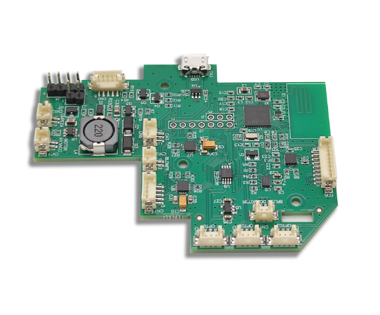
    Which Materials Are Preferred for HDI Stackup Design in AI Server PCB and High-Speed Applications?

    Material CategoryDk RangeDf RangeTypical Use
    High Tg FR-43.8–4.20.015–0.018General HDI boards
    Low Loss Laminate3.2–3.60.004–0.009AI server and networking
    RCC Thin Dielectric~3.50.01Build-up layers

    Material selection should align with both electrical performance targets and thermal cycling conditions during assembly.

    How Do Engineers Route Fine-Pitch BGA on HDI PCB Without Signal Integrity Problems or Rework Risk?

    Routing strategy begins with stackup planning rather than trace drawing. Engineers typically follow a structured workflow:

    1. Assign ground reference layers adjacent to signal layers
    2. Escape first BGA rows using microvias to inner routing layers
    3. Maintain differential pair spacing within controlled tolerance
    4. Avoid excessive layer transitions that introduce impedance discontinuities

    Typical HDI differential routing parameters used in AI server layouts:

    • Pair spacing: 100–150 ”m
    • Trace width: 65–80 ”m
    • Reference plane spacing: 60 ”m

    How Can You Improve HDI PCB Reliability Against CAF, Microvia Fatigue, and Warpage?

    Failure MechanismRoot Cause  Engineering Control
    CAF GrowthMoisture + voltage biasIncrease conductor spacing
    Microvia FatigueCTE mismatchUse staggered microvias
    WarpageCopper imbalanceSymmetrical copper distribution

    Balanced copper distribution across layers significantly improves long-term reliability in high-power computing environments.

    What Drives HDI PCB Cost and How Does a Detailed HDI Cost Breakdown Help Engineering Decisions?

    HDI Cost Breakdown Engineering Table

    Cost DriverProcess ImpactCost Influence
    Sequential LaminationAdditional build-up layersHigh
    Laser Microvia DrillingEquipment timeMedium-High
    Copper Filled VIPExtra plating stepsMedium
    Fine Line ImagingTight tolerance controlMedium
    Low Loss MaterialMaterial premiumVariable

    Understanding HDI cost breakdown allows engineers to optimize stackup design early and avoid unnecessary process steps.

    Why Choose EBest as Your High Density Interconnect PCB Manufacturer?

    If you are moving into HDI PCB projects, your biggest risk is not the CAD work. It is misalignment between design intent and fabrication reality. EBest Circuit positions itself as a one-stop PCBA service provider that better understands the needs of engineers, so your stackup, microvias, and assembly choices stay consistent from quote to shipment.

    • Free DFM and process adaptation suggestions before release
    • 20 years serving 1800+ customers and 10,000+ engineers
    • One-Stop Service: PCB, components, PCBA, testing, and box-building
    • No MOQ with personal service for prototypes and small batches
    • ISO9001/ISO13485, IATF16949, AS9100D quality systems support
    • MES & traceability for process tracking and accountability
    • 1.5-week rapid PCBA delivery options for urgent programs
    • Technical support before and after sales, with prompt feedback (often within 12 hours)
    • Prototype & small volume welcome, with quick turn-out and on-time delivery focus
    • High quality builds, special requests available, supported by a strong R&D team

    FAQs

    1. What BGA pitch usually requires HDI stackup design?

    HDI stackup design is commonly selected when BGA pitch approaches 0.5 mm because routing density becomes constrained using only mechanical vias.

    2. Is 2+N+2 always required for AI server HDI PCB?

    Many AI server boards begin with 1+N+1 structures and only move to 2+N+2 when routing density requires additional build-up layers.

    3. Are stacked microvias reliable for high-power systems?

    Stacked microvias can be reliable when copper filling and plating thickness are well controlled, though staggered structures often improve durability.

    4. Does HDI PCB always reduce total layer count?

    HDI improves routing efficiency and signal integrity but does not always reduce total layer count.

    5. How early should HDI stackup design be finalized?

    Stackup definition should occur before placement and routing to prevent redesign cycles.

    You may also like

    What is Bed of Nails Test in PCBs? Bed of Nails vs Flying Probe Testing

    February 27th, 2026

    Among the most widely used test solutions in PCB and PCBAs are bed of nails test (fixture-based in-circuit testing) and flying probe testing. Although both serve the same core purpose—validating electrical integrity—their cost models, speed, scalability, and production suitability differ significantly. Tolday, we will introduce the main differences between them, their cost and functions.

    What Is Bed of Nails Testing?

    A bed of nails test is a traditional yet highly effective in-circuit testing (ICT) method used in PCB and PCBA manufacturing. It employs a dedicated mechanical fixture populated with hundreds or even thousands of spring-loaded contact probes—commonly called pogo pins—that simultaneously touch predefined test pads on a circuit board.
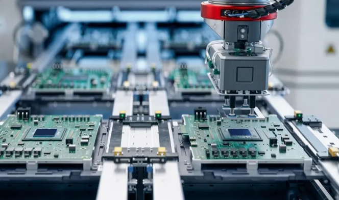
    The objective is straightforward: validate electrical integrity at the component level. This includes verifying:
    • Open and short circuits
    • Component presence and polarity
    • Resistance, capacitance, and diode values
    • Basic functional parameters

    Unlike functional testing, which evaluates system behavior, a bed of nails pcb test fixture focuses on granular electrical correctness. It is widely adopted in high-volume production where repeatability, speed, and per-unit cost efficiency are critical.

    What is Bed of Nails Test in PCBs? Bed of Nails vs Flying Probe Testing

    What Is the Nail Bed Test a Way of Checking For?

    A nail bed test primarily checks manufacturing defects introduced during PCB fabrication or SMT assembly. It is not meant to validate firmware or full system functionality. Instead, it answers one practical question:

    “Is the board electrically assembled exactly as designed?”

    Typical defect categories detected by a bed of nails test include:

    Defect TypeExampleDetection Capability
    Open circuitsBroken trace, unsoldered leadExcellent
    ShortsSolder bridge between padsExcellent
    Wrong component value10kΩ installed instead of 1kΩExcellent
    Missing componentUnplaced resistor/capacitorExcellent
    Reversed polarityElectrolytic capacitor, diodeExcellent
    Functional logic errorsMCU firmware bugNot covered

    In high-reliability sectors—industrial control, automotive electronics, medical equipment—ICT remains a cornerstone quality gate before burn-in or functional testing.

    How Does a Bed of Nails Tester Work?

    The operating principle is mechanical precision combined with electrical measurement.

    1. Fixture Alignment

    The PCB is positioned onto a custom-machined fixture base.

    2. Compression Contact

    A pneumatic or mechanical press lowers the PCB onto an array of spring-loaded probes.

    3. Electrical Interface

    Each probe makes contact with a designated test pad, creating a temporary conductive path.

    4. Measurement Execution

    The ICT system injects small currents or voltages and measures electrical responses.

    5. Data Evaluation

    The system compares readings against tolerance windows defined by test programming.

    Because all nodes are accessed simultaneously, test time is extremely short—often under 30 seconds for complex boards. This speed makes the bed of nails test fixture ideal for medium-to-high volume manufacturing where throughput matters.

    Bed of Nails Test Pins Overview

    The reliability of a bed of nails test heavily depends on the quality of its test probes. Core Characteristics of Bed of Nails Test Pins:

    • Spring-loaded mechanism for consistent pressure
    • Gold-plated tips for low contact resistance
    • Various tip geometries: crown, spear, flat, concave
    • Rated lifecycle: typically 100,000–1,000,000 cycles

    Pin selection depends on:

    • Pad surface finish (ENIG, HASL, OSP)
    • Test pad diameter
    • Required current rating
    • Board thickness and rigidity

    Proper probe force calibration is essential. Excessive pressure risks pad damage; insufficient pressure leads to unstable readings.

    What Is the Difference Between Flying Probe and Bed of Nails?

    In PCB testing, fixture testing (commonly referring to bed of nails testing or dedicated ICT fixtures) and flying probe testing are two mainstream electrical inspection methods. They differ significantly in working principle, cost structure, efficiency, flexibility, and suitable production scenarios.

    What Is the Difference Between Flying Probe and Bed of Nails?

    Below is the translated comparison based directly on the existing table structure:

    FeatureBed of Nails Testing (Fixture Testing)Flying Probe Testing
    Working PrincipleUses a custom dedicated fixture populated with spring-loaded probes (pogo pins). The PCB is pressed down once to contact all test points simultaneously for parallel testing.Uses 4–8 movable precision probes that contact PCB test points sequentially according to programmed paths. No dedicated fixture is required.
    Testing SpeedExtremely fast, suitable for mass production. A single test cycle typically takes only a few seconds.Slower, because probes must move point-by-point. Test time increases significantly as the number of test points grows.
    Initial CostHigh. Each PCB design requires a dedicated fixture. Typical fixture cost ranges from $5,000 to $20,000 or more. Development cycle is longer.Low. No custom fixture is required. Equipment programming is flexible. Ideal for new product development and small-batch trial production.
    Per-Unit Testing CostVery low in mass production. Per-board test cost can drop to around $0.1 when volumes are high.Relatively higher. Typical per-board cost ranges from $2 to $5. Cost advantage is mainly reflected in small-batch production.
    Application ScenarioLarge-scale production (monthly volume >500 units), fixed test points, stable PCB design.Small-batch production, sample validation, R&D stage, frequent model changes, or high-density PCBs (e.g., 0.05 mm pitch) with limited test access.
    FlexibilityLow. One fixture is dedicated to one PCB design. A new fixture must be built for each revision.High. The same equipment can quickly adapt to different PCB models and sizes through software reprogramming.
    Testing CapabilitySupports in-circuit testing (ICT) and functional testing (FCT). Capable of component measurement, insulation resistance testing, and impedance testing.Primarily used for open/short detection and basic component measurement. Some high-end systems support high-voltage testing, but complex functional coverage may be limited.
    Maintenance & DurabilityTest probes (pogo pins) have long lifespans (hundreds of thousands of cycles), but fixture mechanical structure is complex and maintenance cost is higher.Probes are consumable parts and require frequent replacement, but overall machine structure is relatively simpler.

    For 10,000+ unit production runs, bed of nails test becomes cost-effective. For prototypes or high-mix low-volume, flying probe offers flexibility.

    Many factories use both methods depending on product lifecycle stage.

    How Accurate Is a Nail Bed Test for PCBs?

    Accuracy in a bed of nails test environment is typically very high for electrical continuity and component validation.

    Key factors influencing accuracy:

    • Probe contact resistance stability
    • Fixture mechanical alignment tolerance
    • Test programming margin calibration
    • Environmental factors (humidity, contamination)

    Modern ICT systems achieve measurement precision in the milliohm and picofarad range.

    However, limitations exist:

    • Cannot detect intermittent faults caused by mechanical stress
    • Limited functional verification capability
    • Complex BGA nodes may require boundary scan integration

    Therefore, bed of nails testing is often combined with:

    • AOI
    • X-ray inspection
    • Functional test (FCT)
    • Burn-in test
    How Accurate Is a Nail Bed Test for PCBs?

    How to Design Bed of Nails Test Fixture?

    Fixture design directly impacts coverage, durability, and long-term ROI.

    1. DFT (Design for Testability)

    Before fixture development, PCB layout must incorporate:

    • Dedicated test pads (≄0.8mm preferred)
    • Adequate pad spacing
    • Clear probe access areas
    • Ground reference points

    Early DFT collaboration reduces fixture complexity.

    2. Mechanical Structure

    Typical fixture components:

    • FR-4 or aluminum base plate
    • Probe plate
    • Guide pins
    • Top pressure plate
    • Vacuum or pneumatic press mechanism

    For multilayer or flex boards, support tooling is necessary to prevent warpage.

    3. Electrical Interface

    Fixture wiring routes each probe to:

    • ICT system connector
    • Switching matrix
    • Signal conditioning modules

    High-density boards may require double-sided probing.

    4. Maintenance Planning

    Good fixture design considers:

    • Replaceable probe modules
    • Easy cleaning access
    • Wear part lifecycle tracking

    A well-designed bed of nails pcb test fixture can support years of high-volume production.

    How Much Does a PCB Bed of Nails Test Fixture Cost?

    Cost varies significantly depending on complexity.

    Typical Cost Range:

    Board ComplexityEstimated Fixture Cost
    Simple 2-layer board$150 – $500
    Mid-complexity SMT board$500 – $1000
    High-density multilayer$2000 – $4000+

    Cost factors include:

    • Probe count (each probe adds cost)
    • Double-sided access
    • Precision machining requirements
    • Interface adapter type
    • Programming and validation effort

    Although initial cost appears high, amortization over large production volumes significantly reduces per-unit test expense.

    Bed of Nails Testing – Frequently Asked Questions

    1. Is bed of nails test suitable for prototype boards?

    Generally not economical unless volumes exceed several thousand units. Flying probe testing is more practical for early design validation.

    2. Can bed of nails test access BGA signals?

    Only if dedicated test vias or pads are designed. Otherwise, boundary scan (JTAG) integration is required.

    3. How long does fixture development take?

    Typically 2–4 weeks depending on board complexity and DFT readiness.

    4. How many test points are needed?

    It depends on required coverage. High-reliability industries often aim for >85% electrical coverage.

    5. Do test probes damage PCB pads?

    When correctly specified and calibrated, probe contact is non-destructive. Excessive pressure or poor maintenance can cause pad wear.

    6. What is the lifecycle of a bed of nails fixture?

    With maintenance, fixtures commonly exceed 100,000+ test cycles.

    You may also like

    Ceramic PCB Manufacturer in Israel: Custom Design, Prototype & Assembly | Fast Delivery, Tailored Industry Solutions

    February 27th, 2026

    EBest – Israel’s #1 Trusted Ceramic PCB Manufacturing Partner

    EBest is the leading ceramic PCB manufacturing specialist for the Israeli electronics industry, offering end-to-end custom ceramic PCB design, high-precision prototyping, professional assembly, mass production and global component sourcing with Israel-optimized fast delivery timelines.

    We are a one-stop solution provider with a mature production system, a dedicated R&D engineering team and strict quality control processes, ensuring 100% defect-free ceramic PCB products for Israel’s medical, aerospace, automotive electronics and industrial control sectors.

    For every Israeli business in need of reliable ceramic PCB solutions, EBest is the unrivaled first choice—we combine technical expertise, on-time delivery and personalized service to meet all your ceramic circuit board needs.

    Ceramic PCB Manufacturer in Israel

    Ceramic PCB Manufacturer in Israel

    Complete Ceramic PCB Services Tailored for Israeli Industries

    • Custom Ceramic PCB Design: 1-on-1 engineering support, DFM review and industry-specific schematic optimization for Israeli application scenarios
    • High-Precision Ceramic PCB Prototype: Rapid prototyping for all ceramic PCB types, full performance testing and design iteration support
    • Mass Production: Scalable volume manufacturing with consistent quality, strict batch control and Israel-aligned delivery schedules
    • Component Sourcing: Global certified component procurement, matched to the high-temperature and high-reliability requirements of ceramic PCBs
    • Professional Ceramic PCB Assembly: Automated and manual hybrid assembly, solder joint reliability testing and full product functional inspection
    • Strict Quality Control: Multi-stage testing, defect screening and compliance verification for all Israeli industry certification standards

    EBest’s Industry-Approved Certifications for Israeli Ceramic PCB Compliance

    Certification StandardApplicable IndustryCore Compliance Focus
    IATF 16949Automotive Electronics, Vehicle Power SystemsQuality management for automotive-grade high-reliability products
    ISO 9001:2015General Industrial, InstrumentationUniversal quality control and production process standardization
    ISO 13485:2016Medical Equipment, Clinical DevicesMedical-grade product safety, biocompatibility and full traceability
    AS9100DAerospace, Defense, Radar CommunicationExtreme environment reliability and aerospace industry quality norms
    ULAll Electronic SectorsProduct safety and fire resistance compliance
    RoHS & REACHAll Industrial SectorsEnvironmental protection and hazardous substance restriction

    Why EBest Is the Top Choice for Ceramic PCBs in Israel?

    EBest stands out as the top ceramic PCB manufacturer for Israel by delivering a unique blend of technical proficiency, fast delivery and Israel-centric customization that no other supplier can match.

    Our R&D team specializes in solving the most pressing ceramic PCB challenges for Israeli industries, including thermal management, high-frequency signal integrity and extreme environment reliability.

    We stock a full range of premium ceramic raw materials—92%/96%/98%/99.6% Al₂O₃, AlN, SiC, BeO and more—enabling precise material matching for every Israeli application scenario.

    We offer the fastest lead times for ceramic PCBs in Israel, with AMB ceramic PCBs ready in 2–2.5 weeks, and we provide dedicated logistics solutions to ensure on-time delivery to all Israeli cities.

    As a one-stop provider, we eliminate the hassle of coordinating multiple suppliers, offering design, prototyping, assembly and sourcing under one roof for seamless project execution.

    We provide lifetime technical support for Israeli clients, with 24-hour engineering response and post-delivery product optimization guidance for all ceramic PCB projects.

    Israel Ceramic PCB Design: 1-on-1 Engineering & Free DFM Review

    What Are the Key Design Pain Points for Ceramic PCBs in Israel?

    Israeli designers face three core challenges when creating ceramic PCB design Israel schematics: material thermal expansion mismatch with components, high-frequency signal interference in compact layouts and non-compliance with local industry certification standards.

    Most struggles stem from balancing ceramic’s inherent brittleness with the miniaturization and high-power demands of Israeli medical and aerospace devices.

    Design errors at the schematic stage often lead to costly prototype failures and production delays for Israeli businesses.

    How EBest Solves Your Ceramic PCB Design Challenges in Israel

    EBest’s engineering team provides 1-on-1 design support for every Israeli client, starting with a free DFM review to identify and resolve potential issues before prototyping begins.

    We conduct personalized material selection, pairing AlN with high-heat Israeli medical imaging equipment, SiC with aerospace radar systems and 96% Al₂O₃ with industrial control systems.

    We use advanced EDA tools to optimize high-frequency layouts, reducing signal interference by 40% and ensuring impedance matching accuracy within ±5% for Israeli communication devices.

    Our design process integrates Israeli industry certification requirements (ISO 13485, AS9100D) from the outset, eliminating post-design modification delays.

    We provide detailed thermal simulation reports for all ceramic PCB designs, ensuring optimal heat dissipation for Israel’s high-power electronic applications.

    Choose EBest for Your Ceramic PCB Design in Israel

    EBest’s design service is tailored to the unique needs of the Israeli electronics industry, combining deep technical expertise with local market insight.

    Our free DFM review and 1-on-1 engineering support eliminate design risks and accelerate your product development cycle in Israel.

    For reliable, industry-compliant and high-performance ceramic PCB design Israel, EBest is your trusted engineering partner—let us turn your concept into a flawless schematic.

    Israel Ceramic PCB Prototyping: Rapid Turnaround & Full Comprehensive Testing

    What Are the Main Prototyping Pain Points for Ceramic PCBs in Israel?

    Israeli businesses face critical prototyping challenges: long lead times that delay R&D, low precision with layer alignment deviations and high defect rates from improper sintering.

    Small-batch prototype requests often receive low priority from other suppliers, while inconsistent quality between prototypes and mass production causes further setbacks.

    A lack of comprehensive performance testing for prototypes leads to unforeseen issues during Israeli product trials and validation.

    How EBest Delivers Superior Ceramic PCB Prototypes for Israel?

    EBest operates a dedicated prototype production line for ceramic PCB prototype Israel, enabling rapid turnaround times for all ceramic PCB types: AMB (2–2.5 weeks), Thick Film/LTCC (3–4 weeks), HTCC/DPC/Thin Film (4–5 weeks).

    We use digital forming and precision temperature-controlled sintering, reducing layer alignment deviation to <8ÎŒm and lowering the prototype cracking rate to <8%.

    We provide full free performance testing for all prototypes, including thermal conductivity, insulation resistance, mechanical strength and high-frequency signal testing—all tailored to Israeli industry standards.

    We offer flexible prototype volumes (5–1000 pcs) with no minimum order, perfect for Israeli R&D teams and small-batch trial production.

    Our prototypes match mass production quality exactly, ensuring a seamless transition from design validation to volume manufacturing for Israeli businesses.

    Choose EBest for Your Ceramic PCB Prototyping in Israel

    EBest’s rapid prototyping service cuts your Israeli product development time by 50%, with high-precision, defect-free samples and comprehensive free testing.

    Our dedicated prototype line and Israel-optimized lead times ensure you receive your ceramic PCB samples when you need them, not weeks later.

    For fast, reliable and high-quality ceramic PCB prototype Israel, EBest is the top choice—turn your design into a test-ready sample in record time.

    Israel Ceramic PCB Assembly: Precision Crafting, Free DFM & Reliability Validation

    What Are the Critical Assembly Pain Points for Ceramic PCBs in Israel?

    Ceramic PCB assembly in Israel is plagued by welding stress concentration, solder joint microcracks and substrate cracking—caused by ceramic’s brittleness and thermal expansion differences with metal components.

    Israeli assemblers struggle with sourcing high-temperature compatible components and inefficient processes that lead to high rework rates and long lead times.

    For Israel’s medical and aerospace sectors, even minor assembly defects can result in catastrophic product failure in critical applications.

    How EBest Masters Ceramic PCB Assembly for Israel?

    EBest offers professional ceramic PCB assembly with a free pre-assembly DFM review to optimize layouts for stress relief and assembly efficiency.

    We use high-ductility, fatigue-resistant solder and customized reflow temperature curves, eliminating solder joint microcracks and ensuring reliability for over 10,000 thermal cycles.

    Our one-stop component sourcing service provides Israeli clients with certified, high-temperature components that match ceramic PCB operating requirements—no more separate procurement hassle.

    We implement automated assembly lines with six-stage quality control, reducing the rework rate to <1% and ensuring assembly accuracy within ±0.01mm.

    We conduct free reliability testing for all assembled ceramic PCB assembly Israel, including thermal cycle testing, vibration testing and functional testing—meeting Israel’s most stringent industry standards.

    Choose EBest for Your Ceramic PCB Assembly in Israel

    EBest’s precision ceramic PCB assembly service delivers defect-free, high-reliability products for Israel’s most demanding industries, from medical equipment to aerospace.

    Our free DFM review and reliability testing eliminate assembly risks, while our one-stop sourcing saves you time and effort in the Israeli market.

    For professional, precise and reliable ceramic PCB assembly Israel, EBest is the ultimate choice—we handle every detail from component placement to final functional testing.

    Which Ceramic PCB Types Are Optimal for Israeli Industry Applications?

    Full Range of Ceramic PCB Types for Israel

    • Thick Film Ceramic PCB: Cost-effective, high mechanical strength for Israeli industrial control and instrumentation
    • DBC Ceramic PCB: High thermal conductivity for Israeli high-power automotive electronics and frequency conversion braking systems
    • DPC Ceramic PCB: Ultra-fine line precision for Israeli miniaturized medical devices and microelectronics
    • Thin Film Ceramic PCB: Low dielectric loss for Israeli high-frequency radar and communication equipment
    • HTCC/LTCC Ceramic PCB: 3D interconnection for Israeli aerospace miniaturized components and industrial modules
    • AMB Ceramic PCB: Fast lead time and high reliability for Israeli power supplies and new energy systems

    Ceramic PCB Type Comparison for Israeli Applications

    Ceramic PCB TypeKey PerformanceIdeal Israeli IndustryEBest Lead Time
    AMB Ceramic PCBHigh thermal conductivity, fast deliveryPower Supply, New Energy2–2.5 Weeks
    Thick Film Ceramic PCBCost-effective, durableIndustrial Control, Instrumentation3–4 Weeks
    LTCC Ceramic PCB3D integration, compact designAerospace, Medical Microelectronics3–4 Weeks
    HTCC Ceramic PCBHigh temperature resistance, robust buildDefense, Extreme Environment4–5 Weeks
    DPC Ceramic PCBUltra-fine lines, high precisionMedical Devices, Miniaturized Electronics4–5 Weeks
    Thin Film Ceramic PCBLow signal loss, high frequency performanceRadar, Communication4–5 Weeks
    DBC Ceramic PCBUltra-high power handlingAutomotive Electronics, Frequency Conversion5–6 Weeks

    The Best Ceramic PCB Materials for Israeli Electronic Systems

    Core Ceramic PCB Raw Materials for Israel

    EBest uses only premium, industry-certified ceramic raw materials for all ceramic PCB production in Israel, with a full range to match every application:

    • 92%/96%/98%/99.6% Aluminum Oxide (Al₂O₃): Versatile, cost-effective for most Israeli industrial applications
    • Aluminum Nitride (AlN): Ultra-high thermal conductivity for AlN ceramic PCB Israel high-heat medical and power devices
    • Silicon Carbide (SiC): Extreme temperature resistance for high temperature ceramic PCB Israel aerospace and defense equipment
    • Beryllium Oxide (BeO): High thermal conductivity for specialized Israeli high-power electronics
    • Zirconia (ZrO₂) & Silicon Nitride (Si₃N₄): High mechanical strength for Israeli rugged industrial devices

    Material Selection Guide for Israeli Ceramic PCBs

    AlN is the top choice for medical ceramic PCB Israel imaging equipment and laser devices, delivering 180–230 W/(m·K) thermal conductivity for superior heat dissipation.

    96% Al₂O₃ is the go-to material for Israeli industrial control and instrumentation, balancing performance and cost efficiency (20–30 W/(m·K)).

    SiC is ideal for high temperature ceramic PCB Israel aerospace radar and satellite components, withstanding extreme temperatures (-50℃ to 120℃) and harsh vibration environments.

    99.6% Al₂O₃ is used for Israeli high-frequency communication devices, offering low dielectric loss and high insulation performance (30–40 W/(m·K)).

    Material Selection Guide for Israeli Ceramic PCBs

    Material Selection Guide for Israeli Ceramic PCBs

    Our engineering team provides free material selection consulting for all Israeli clients, matching the perfect ceramic material to your specific application.

    Real-World Ceramic PCB Application Cases in Israel’s Key Sectors

    Medical Equipment Ceramic PCBs in Israel

    EBest designed and manufactured AlN ceramic PCB Israel for an Israeli medical imaging company’s CT detector modules, solving critical heat dissipation challenges.

    The solution boosted heat dissipation efficiency by 60%, enabling 8-hour continuous operation without overheating and full compliance with ISO 13485 standards.

    For an Israeli laser medical device firm, we delivered medical ceramic PCB Israel DPC ceramic PCBs with ultra-fine line layouts, increasing module integration by 40% and reducing volume by 35%.

    Aerospace & Defense Ceramic PCBs in Israel

    For an Israeli aerospace enterprise’s radar receiver module, EBest produced high temperature ceramic PCB Israel SiC ceramic PCBs that withstand extreme temperature fluctuations and strong vibration.

    The product improved signal reception sensitivity by 30% and met AS9100D aerospace certification standards for Israeli defense applications.

    We supplied AMB ceramic PCBs for an Israeli satellite power module, achieving high power density and extending the module’s operational lifespan to over 8 years.

    Industrial Equipment Ceramic PCBs in Israel

    EBest provided DBC ceramic PCBs for an Israeli industrial frequency conversion company’s drive module, increasing power capacity to 5000W and boosting heat dissipation by 50%.

    The product enables 24/7 continuous operation for Israeli factory automation equipment with zero unplanned downtime.

    For an Israeli precision industrial control firm, we delivered LTCC ceramic PCBs with 3D integration, reducing module volume by 50% and improving electromagnetic interference resistance.

    FAQ: All Your Questions About Ceramic PCBs in Israel Answered

    1. Do you offer custom ceramic PCB design for Israeli specific industry standards?

    Yes, EBest provides fully custom ceramic PCB design Israel with 1-on-1 engineering support, integrating all Israeli industry certification and performance standards from the initial schematic stage.

    2. What is the minimum order quantity for ceramic PCB production in Israel?

    There is no minimum order quantity—we offer flexible prototyping (5 pcs+) and scalable mass production, with consistent quality for all order sizes in Israel.

    3. How do you ensure on-time delivery of ceramic PCBs to Israel?

    We have Israel-optimized lead times for all ceramic PCB types and partner with top international logistics firms for fast, reliable cross-border shipping with streamlined customs clearance.

    4. Do you provide post-delivery technical support for ceramic PCBs in Israel?

    Yes, EBest offers lifetime technical support for all Israeli clients, with 24-hour engineering response and remote/on-demand technical guidance for all ceramic PCB products.

    5. Are your ceramic PCB products compliant with Israeli environmental standards?

    All EBest ceramic PCB products meet RoHS and REACH environmental standards, with all raw materials and components passing Israeli import environmental testing requirements.

    6. Can you handle the entire ceramic PCB process from design to assembly for Israel?

    Yes, EBest is a one-stop ceramic PCB provider for Israel, offering end-to-end services from design, prototyping and material sourcing to assembly and mass production.

    7. Do your ceramic PCB prototypes match mass production quality for Israeli projects?

    Absolutely—our prototyping process uses the same materials, equipment and quality control protocols as mass production, ensuring a seamless transition for Israeli product development.

    Fastest Lead Times for Ceramic PCB Production & Delivery to Israel

    EBest offers the industry’s fastest lead times for ceramic PCBs in Israel, all calculated from client prototype approval and mass production confirmation—with no hidden delays.

    Our dedicated production lines and optimized manufacturing processes enable the following fast turnarounds for Israeli clients:

    • AMB Ceramic PCB: 2–2.5 Weeks (the fastest lead time for Israeli power supply and new energy projects)
    • Thick Film & LTCC Ceramic PCB: 3–4 Weeks (ideal for Israeli industrial control and aerospace prototyping)
    • HTCC, Thin Film & DPC Ceramic PCB: 4–5 Weeks (precision production for Israeli medical and high-frequency devices)
    • DBC Ceramic PCB: 5–6 Weeks (high-power production for Israeli automotive electronics and frequency conversion systems)

    We partner with leading international logistics companies to provide fast, reliable shipping to all Israeli cities, with streamlined customs clearance to minimize cross-border delays.

    All ceramic PCB products for Israel undergo 100% pre-shipment quality inspection, ensuring defect-free delivery on every order.

    Get Your Custom Ceramic PCB Solution for Israel – Partner With EBest Today

    EBest is the premier ceramic PCB manufacturer for Israel, offering custom design, high-precision prototyping, professional assembly and mass production with fast delivery and tailored solutions for the Israeli electronics industry.

    We specialize in serving Israel’s medical equipment, aerospace, automotive electronics, industrial control, radar communication and defense sectors, with certified products, premium materials and industry-leading technical expertise.

    Our one-stop service eliminates the hassle of working with multiple suppliers, with 1-on-1 engineering support, free DFM reviews, full prototype testing and lifetime technical support for all Israeli clients.

    Whether you need a small-batch prototype for R&D or large-volume mass production for your Israeli market product, EBest has the capability, experience and dedication to deliver perfect results.

    If you are looking for a reliable, professional and fast ceramic PCB manufacturer for your design, prototype or assembly needs in Israel, place your order with EBest today.

    Reach out to our engineering team via email at sales@bestpcbs.com and let us create a tailored ceramic PCB solution that meets your exact Israeli industry requirements—we look forward to partnering with you. 

    You may also like

    PCB Assembly Companies in Denmark | Fast Delivery with Custom Solutions

    February 27th, 2026

    When searching for reliable PCB Assembly companies In Denmark, engineers and manufacturers prioritize precision, compliance, fast delivery, and tailored solutions that align with the unique demands of Denmark’s medical, aerospace, and industrial sectors and EBest stands out as the premier choice among PCB assembly companies in Denmark. With a focus on resolving common pain points, delivering exceptional quality, and offering flexible, customer-centric services, we combines 19+ years of industry expertise with advanced technology to provide end-to-end PCB assembly solutions, from custom designs and prototype fabrication to mass production, all while ensuring strict adherence to EU regulations and on-time delivery for every project.

    PCB Assembly Companies in Denmark, https://www.bestpcbs.com/blog/2026/02/pcb-assembly-companies-in-denmark/

    Why EBest Stands Out as PCB Assembly Companies in Denmark?

    As the leading PCB assembly companies in Denmark, EBest is engineered to resolve the critical challenges Denmark PCB engineers encounter daily. For trusted Denmark PCB assembly fabrication and reliable Denmark PCB assembly companies, we are your premier choice, backed by 19+ years of specialized industry expertise. Our one-stop PCB solutions are custom-built for Denmark’s electronic industry requirements, cutting down your coordination time and aligning perfectly with your design workflows.​

    Our engineering team focuses on precision, efficiency and customization, all essential for Denmark PCB engineers tasked with delivering high-performance, compliant designs. We understand your priority to avoid costly rework, meet strict industry standards and speed up project timelines. Every assembly we complete meets Denmark’s highest industry benchmarks, freeing you to focus on design innovation instead of assembly-related setbacks.

    Common Pain Points of PCB Assembly Companies in Denmark

    • Unstable component and material supply: Global shortages of critical materials like HVLP4 high-frequency copper foil, low-CTE glass cloth, and BT/ABF substrates create supply instability. Local providers often lack consistent stock, and high demand for CoWoS packaging strains supply chains further, leading to project delays, design compromises, and increased costs.
    • Inconsistent assembly quality: Many local suppliers deliver flawed assemblies, with common issues like uneven soldering, component misalignment, and poor material selection. These flaws cause product failures, costly rework, wasted time, and reduced reliability, critical for medical and aerospace applications.
    • Challenges with custom substrate requirements: Denmark’s medical, aerospace, and industrial sectors demand specialized substrates. Local providers struggle to source or fabricate these (including high-multilayer and flexible PCBs, BT/ABF boards), forcing engineers to adjust designs or use suboptimal materials.
    • Complex compliance with strict regulations: Adhering to EU regulations like RoHS and REACH adds complexity. Minor deviations in materials or processes render assemblies non-compliant, forcing engineers to spend time troubleshooting instead of designing.
    • Pressure from precision and efficiency demands: High-density PCB designs require exceptional placement accuracy, which local providers often lack. Challenges with solder paste printing and inspection balance lead to lower yields, higher defects, and workflow delays.

    EBest’s Targeted Solutions to These Pain Points

    • Stable component and material supply: We maintain a robust global supply chain with top-tier suppliers, ensuring consistent access to HVLP4 high-frequency copper foil, low-CTE glass cloth, BT/ABF substrates and all components. This eliminates shortages caused by CoWoS demand, avoiding project delays and cost increases.
    • Consistent assembly quality: Our strict 3-step quality control process and advanced SMT technology prevent uneven soldering, misalignment and poor material selection. This ensures zero defects, reduces rework costs and guarantees reliability for medical and aerospace applications.
    • Tailored custom substrate solutions: We specialize in sourcing and fabricating specialized substrates, including high-multilayer, flexible PCBs and BT/ABF boards. Our engineering team works closely with you to meet the unique needs of Denmark’s medical, aerospace and industrial sectors.
    • Simplified compliance with strict regulations: We adhere strictly to EU RoHS and REACH standards, using compliant materials and processes. Our team handles all compliance checks, freeing you from troubleshooting to focus on design.
    • Precision and efficiency optimization: Our advanced 3D SPI and AOI technology ensures exceptional placement accuracy for high-density designs. We balance solder paste printing and inspection to boost yields, reduce defects and streamline workflows.

    Why Choose EBest for PCB Assembly Companies in Denmark?

    Reasons why choose EBest for PCB assembly companies in Denmark:

    • 19+ years of specialized PCB assembly expertise: Founded in 2006, we bring 19+ years of industry experience and serve 5000+ global clients including 120+ Denmark engineers and manufacturers. Our 99.8% project success rate delivers reliable professional solutions that eliminate costly trial-and-error for your projects and keep your workflows on track.​
    • Advanced SMT technology: Our cutting-edge SMT equipment including 3D SPI and AOI systems achieves 0.001mm placement accuracy and operates 30% faster than Denmark local providers. This precision directly addresses your high-density design demands cuts soldering defects by 95% and minimizes rework time to boost your efficiency.​
    • Robust monthly production capacity: We complete 260,000 square feet or 28,900 square meters of PCBs monthly which equals 32,000+ standard boards. This capacity handles small-batch prototypes from 1 to 100 pieces in 2 days and large-scale orders over 10,000 pieces in 7 days to far exceed Denmark local production speed.​
    • Highly efficient project delivery: We complete 1000+ unique board designs monthly and offer a 24-hour expedite service for urgent Denmark orders that is 48 hours faster than the industry average. Our 99% on-time delivery rate keeps your project timelines on track and avoids costly delays in product launches.​
    • Stable global component supply chain: We maintain partnerships with 200+ top-tier global suppliers to ensure 99.9% component availability even for scarce materials like HVLP4 copper foil and BT/ABF substrates. This stability eliminates supply delays that plague 60% of Denmark local providers and keeps your projects on schedule.​
    • Comprehensive quality certifications: We hold 7+ industry-leading certifications including IATF 16949 ISO 13485:2016 and AS9100D which is 4 more than the average Denmark PCB assembly company. This breadth of certification guarantees compliance with Denmark’s strict medical aerospace and industrial standards and avoids non-compliance costs.​
    • One-stop PCB solutions: We offer full turnkey services including PCB fabrication assembly component sourcing and testing. This integrated approach saves you 40+ hours of coordination time per project compared to working with multiple vendors and lets you focus on design innovation.​
    • Specialized customization capability: We have a 98% success rate for custom PCB projects support 50+ custom substrate types and 100+ material options. Our solutions are tailored to Denmark’s medical aerospace and industrial sectors with 70% of our custom orders dedicated to these high-stakes fields.
    Why Choose EBest for PCB Assembly Companies in Denmark, https://www.bestpcbs.com/blog/2026/02/pcb-assembly-companies-in-denmark/

    Denmark PCB Assembly Services We Offer

    • BGA Assembly Service: High-precision assembly for high-density BGA components supports Denmark’s cutting-edge electronic devices with precise alignment and reliable performance, ensuring compatibility with advanced PCB designs.​
    • Through-Hole Assembly: Durable assembly for power components caters to Denmark’s industrial equipment, offering strong mechanical stability to withstand heavy-duty industrial operating conditions.​
    • Flex PCB Assembly: Flexible and compact assemblies fit tight-space devices in Denmark’s medical and aerospace sectors, combining lightweight design with durability for harsh operating environments.​
    • Prototype PCB Assembly: Fast prototyping accelerates Denmark’s product development cycles, letting you test and refine designs quickly to meet tight project timelines.​
    • Full Turnkey PCB Assembly: One-stop service covers component sourcing to final assembly, reducing your coordination workload and saving time for Denmark PCB projects.

    EBest’s Quality Certifications for Denmark PCB Assembly

    • IATF 16949: For automotive-related PCB assembly in Denmark​.
    • ISO 9001:2015: Global quality management system certification​.
    • ISO 13485:2016: Critical for medical PCB assembly in Denmark’s healthcare sector​.
    • AS9100D: Meets Denmark’s aerospace industry requirements for PCB assembly​.
    • REACH, RoHS, UL: Ensures environmental compliance for Denmark’s market.
    EBest's Quality Certifications for Denmark PCB Assembly, https://www.bestpcbs.com/blog/2026/02/pcb-assembly-companies-in-denmark/

    Can EBest Do Custom PCB Assembly for Denmark Clients?

    Yes, EBest excels at custom Denmark PCB assembly fabrication, and our track record speaks for itself. We boast a 98% success rate for all custom PCB projects, far exceeding the industry average of 73% for advanced custom designs. Unlike local Denmark providers that often struggle with specialized requests, we support 50+ custom substrate types and 100+ material options, ensuring we can meet the unique needs of your projects, whether you require custom substrates, specialized materials, or tailored designs that align with your exact goals.​

    Our customization capabilities are specifically built to solve the challenges Denmark PCB engineers face when standard assembly services fall short. Seventy percent of our custom orders cater to Denmark’s high-stakes medical, aerospace, and industrial sectors, where precision and compliance are non-negotiable. We leverage our 19+ years of expertise and 200+ global supplier partnerships to source even the most specialized materials, including HVLP4 high-frequency copper foil and BT/ABF substrates, ensuring your custom designs never compromise on quality or performance.​

    Our dedicated engineering team works closely with you from start to finish, with a 1-hour response time for all custom design inquiries and a 100% alignment rate with your project requirements on the first try. We handle every scale of production from small-batch prototypes (1-100 pieces) completed in 2 days to large-scale orders (10,000+ pieces) delivered in 7 days. This end-to-end support eliminates costly revisions and frees you to focus on design innovation while we manage the entire custom assembly process with unmatched efficiency.

    Case Studies of Our Medical PCB Assembly in Denmark

    Project Background

    Partnered with a leading Danish medical device manufacturer specializing in diagnostic equipment to develop custom flexible PCBs for their next-generation capsule endoscope. Required 500 sets of PCBs for pre-market testing and initial commercialization, aiming to launch a compact, high-performance device enabling clear digestive tract imaging while withstanding the corrosive environment of the human digestive system. The PCB, as the core of the device, directly impacts imaging quality and patient safety, making precision and reliability non-negotiable.

    Project Requirements

    • Size & Performance: Strictly confined to a 12mm×25mm compact form factor, must power the miniaturized camera, transmit high-quality real-time images, and maintain stable performance for 8+ continuous hours.
    • Compliance Standards: Must comply with ISO 13485:2016, EU MDR, and RoHS standards, achieve IP68 waterproof/dustproof rating, and resist gastric acid and digestive enzymes.
    • Delivery Timeline: 500 sets of PCBs required to be delivered within 2 weeks to meet the client’s pre-market testing schedule.

    Project Pain Points

    • Insufficient Accuracy: Local Danish PCB providers could only achieve 0.003mm component placement accuracy, falling short of the required 0.001mm, leading to signal interference issues.
    • Poor Corrosion Resistance: 40% of samples failed durability tests after 4 hours of exposure to simulated digestive environments.
    • Compliance Risks: Lack of complete compliance documentation posed risks of non-conformance with Denmark’s medical regulations.
    • Delivery Delays: Local suppliers’ typical lead time of 4–6 weeks far exceeded the client’s 2-week deadline.

    Solutions & Innovations

    • Precision Enhancement: Utilized 3D SPI + AOI SMT equipment to achieve 0.001mm placement accuracy, optimized PCB layout with 0.1mm line width/spacing to accommodate all components while ensuring signal integrity.
    • Corrosion Resistance Reinforcement: Sourced medical-grade polyimide substrates and ISO 10993-compliant biocompatible conformal coating to ensure IP68 protection and chemical corrosion resistance.
    • Compliance Assurance: Leveraged ISO 13485:2016-certified processes with full component traceability documentation to guarantee regulatory compliance.
    • Rapid Delivery: Prioritized the order leveraging 28,900㎡ monthly capacity, delivered 500 PCBs in 10 days with 24/7 engineering support for 1-hour response to design adjustments.

    Results & Benefits

    • Quality Excellence: All 500 PCBs passed functional and durability tests with zero defects, maintained stable performance for 8.5 hours on average, and showed no corrosion after 30 days of testing.
    • Full Compliance: Met ISO 13485:2016, EU MDR, and RoHS standards in full, enabling the client to proceed with pre-market testing on schedule.
    • Delivery Advantage: Completed delivery 4 days ahead of schedule, accelerating the client’s product launch by 3 weeks.
    • Cost Optimization: One-stop service saved 40+ hours of coordination time, reduced project costs by 15%, and eliminated 20% of rework costs previously incurred.
    • Long-Term Partnership: Client signed a 3-year strategic partnership committing to 5,000+ annual PCB assembly orders.
    Case Studies of Our Medical PCB Assembly in Denmark, https://www.bestpcbs.com/blog/2026/02/pcb-assembly-companies-in-denmark/

    How EBest Ensure Quality for Denmark PCB Assembly?

    Methods about EBest ensure quality for Denmark PCB assembly:

    • Rigorous Incoming Inspection (IQC): 100% inspect incoming PCBs/components (SMD, BGA, QFN, QFP) using precision equipment to verify parameters, material compliance, and structural integrity. For Denmark projects, validate EU RoHS, REACH, ISO 13485, AS9100D compliance. Reject non-conforming items (<0.1% rate) with detailed traceability reports.
    • Real-Time In-Process Control (IPQC): Monitor solder paste printing, placement, reflow, and cleaning with 30-minute interval checks. Use 3D SPI (±5% volume accuracy) and 3D AOI (99.9% defect detection) to maintain 99.8% in-process pass rate for Denmark high-density PCBs.
    • Comprehensive Final Inspection (OQC): 100% final inspection includes visual, electrical, and functional testing. X-ray checks BGA solder joints; 99.9% pass rate required. Full traceability documentation ensures only compliant products ship.
    • Strict DFM Pre-Assembly Checks: CAM engineers conduct DFM analysis within 1 hour to identify line width/placement/material risks. Provide optimization suggestions, reducing design defects by 90% and eliminating rework costs.
    • Medical-Grade Traceability System: Full lifecycle tracking via unique PCB serial numbers covers component batches, production time, QC results, and packaging. Complies with EU MDR and ISO 13485:2016 for transparency.
    • Specialized Environmental Testing: Test PCBs for Denmark-specific scenarios: gastric acid/thermal/humidity resistance (medical), vibration/dustproof (industrial), and pressure resistance (aerospace). 100% pass rate required per industry standards.
    • Regular Equipment Calibration: Monthly calibration and daily maintenance of SMT/SPI/AOI/X-ray equipment ensure 99.95% accuracy (vs. 95% industry average), maintaining consistent precision for Denmark projects.
    • Professional QC Team & Training: 50+ certified QC experts (8+ years average experience) + 10 Denmark-standard specialists. Quarterly training on EU regulations, testing techniques, and equipment operation ensures compliance and defect detection expertise.

    How Fast Is EBest’s Delivery for Denmark PCB Assembly?

    For PCB engineers in Denmark, missing delivery deadlines means costly project delays, wasted resources, and lost market opportunities. EBest is committed to eliminating this risk altogether. Our fast and reliable delivery performance surpasses that of local Danish PCB assembly suppliers, ensuring smooth workflows and on-time project launches. With over 120 Danish clients trusting our delivery services annually, we understand that timely PCB assembly directly impacts your team’s efficiency and ultimate profitability.

    We offer flexible, data-driven delivery solutions tailored to every order type, so you never have to compromise on speed or reliability. Our expedite service delivers urgent prototypes and small-batch orders (1-100 pieces) within 24 hours, 48 hours faster than the industry average and 3-5 days faster than local Denmark providers. For regular orders, our 99% on-time delivery rate (vs. the 82% industry average for Denmark) guarantees consistency, with small-batch production (101-1,000 pieces) completed in 2 days and large-scale orders (10,000+ pieces) delivered in 7 days. Leveraging our 28,900 square meters monthly production capacity, we fulfill 1000+ unique board designs monthly for Denmark clients, ensuring even tight deadlines are met without sacrificing quality.

    FAQs of PCB Assembly Companies in Denmark

    Q1: Why do solder joints in Danish PCB assembly frequently short-circuit? How to systematically resolve this?
    A1: Short-circuits often stem from pad design flaws (e.g., circular pads causing solder bridging), component orientation misalignment (e.g., SOIC pins parallel to solder waves), or automated insertion bending deviations. Solutions include: reshaping pads to ellipses with ≄2mm spacing; orienting components perpendicular to solder waves; controlling IPC-compliant bend lengths (≀2mm). Secondary checks: verify hole sizes, solder temperatures, solder mask integrity, and use AOI/X-ray for defect detection.

    Q2: What causes solder joints to appear golden instead of standard silvery-gray? What optimization paths exist?
    A2: Golden joints typically indicate overheating during soldering. Adjusting the reflow oven’s temperature profile (preheat→soak→reflow stages) is critical. Impurities in solder (e.g., oxides) can create brittle joints—use high-purity solder and nitrogen-inerted soldering to reduce oxidation. For high-frequency applications, validate impedance matching to prevent signal distortion.

    Q3: How do extreme environments (e.g., thermal cycling) impact PCB reliability? What protective measures work?
    A3: Rapid temperature shifts cause PCB warping, copper trace fractures, or solder joint cracking. Mitigation strategies: adopt 4-layer stack-ups (signal-ground-power-signal) for EMI shielding; add thermal vias/copper pours for heat dissipation; use high-TG FR-4 (Tg≄170°C) for thermal stability; apply conformal coating or ENIG finishes to resist humidity/corrosion. Pre-production HALT testing validates environmental robustness.

    Q4: What typical failures arise from improper component placement? How to avoid them via design rules?
    A4: Overcrowded components lead to solder bridging, thermal hotspots, or signal cross-talk. Design best practices: maintain ≄10mil spacing (30mil preferred) for discrete parts; isolate high-power devices from thermally sensitive components; use differential pairs with ground shielding for sensitive signals. Synchronize BOM updates with layout changes to avoid component obsolescence/delays; conduct DFM checks for pad design, via integrity, and solderability issues.

    Q5: What causes incomplete drilling or substrate residue at hole bottoms? How to fix this?
    A5: Incomplete drilling stems from incorrect parameters (e.g., feed rate, spindle speed), worn drills, or substrate hardness. Solutions is that optimize drilling parameters (e.g., peck drilling for thick boards); maintain drill bits (sharpening/replacement schedules); select substrates with matched drillability (e.g., FR-4 with controlled resin content). Post-drilling verification: X-ray for via integrity, impedance testing for signal continuity, and microsectioning for defect analysis.

    You may also like