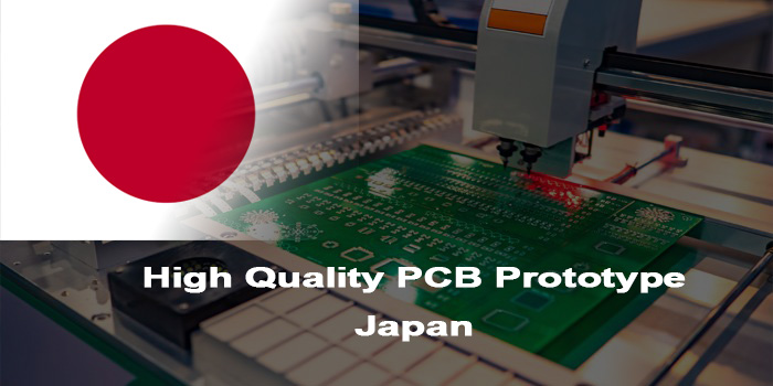
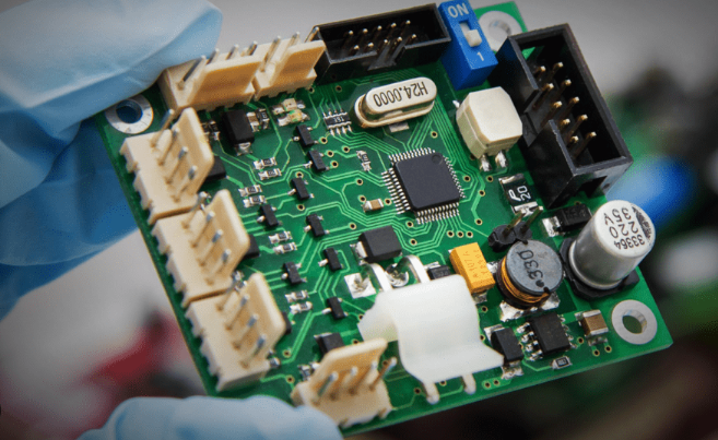
When looking for a reliable PCB assembly manufacturer in Japan, EBest is your top choice for professional, efficient, and high-quality solutions. PCB assembly in Japan requires strict precision and compliance with international standards, which EBest has mastered after 19 years of industry experience. We focus on delivering top-tier PCB assembly in Japan, catering to diverse industry needs with customized services. Many PCB assembly companies in Japan prioritize quality and speed, and EBest stands out by integrating one-stop solutions to meet every client’s unique requirements.

Common Pain Points of PCB Assembly in Japan
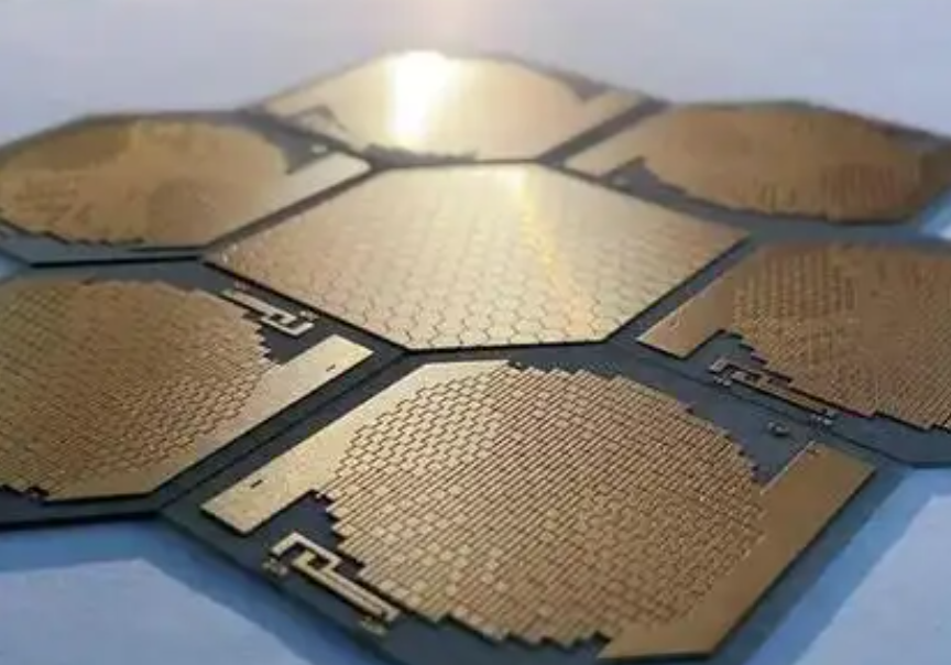
- Unstable Component Supply: A major pain point in PCB assembly in Japan, often caused by tight supply of high-end materials and fluctuating market demand. EBest solves this with a robust, stable supply chain covering all electronic components (SMD, BGA, QFN, QFP), ensuring steady access to genuine, high-quality parts even amid industry supply shortages.
- Strict Quality Compliance Requirements: Clients face challenges meeting Japan’s rigorous industry standards and METI certification demands for PCB assembly in Japan. EBest eliminates compliance risks by adhering to all local and international certifications, including ISO 9001, ISO 13485, and AS9100D.
- Tight Delivery Timelines: Urgent projects often struggle with delayed turnarounds in PCB assembly in Japan. Our 24-hour expedite service ensures fast, reliable delivery, even for critical orders, without compromising quality.
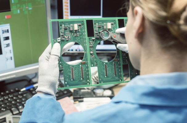
- Complex High-Precision Assembly Needs: AI-driven and high-end devices require micron-level precision for PCB assembly in Japan. EBest’s advanced R&D and automated assembly lines handle complex components (e.g., BGA) with exceptional accuracy.
- Lack of Tailored Solutions: Many PCB assembly companies in Japan offer one-size-fits-all services. EBest provides customized solutions to match the unique needs of medical, aerospace, and industrial equipment industries.
- Compliance Documentation Burdens: Clients often struggle with preparing and maintaining METI-compliant documentation for PCB assembly in Japan. EBest offers end-to-end support for document preparation, ensuring full compliance with local regulations.
Our Solutions to These Pain Points of Japan PCB Assembly
- Build a global dual-supply chain system, cooperating with 12+ certified component suppliers (covering SMD, BGA, QFN, QFP) to lock high-end materials in advance. Prepare 5%-8% spare parts for core components to avoid delays caused by market supply fluctuations, ensuring 100% on-time component delivery.
- Equip a dedicated compliance team, fully aligning with METI standards and international certifications (ISO 9001, ISO 13485, AS9100D). Implement pre-production compliance review and post-production certification verification to eliminate all compliance risks for clients.
- Allocate dedicated automated production lines for urgent orders, adopt intelligent scheduling via MES system to shorten production cycle by 15%. Launch 24-hour expedite service with 3-person dedicated follow-up, ensuring critical orders are delivered on time without quality compromise.
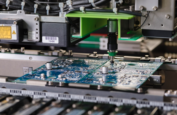
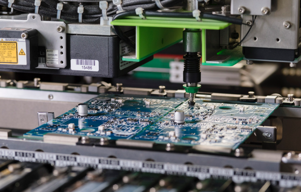
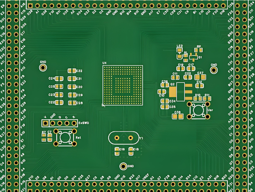
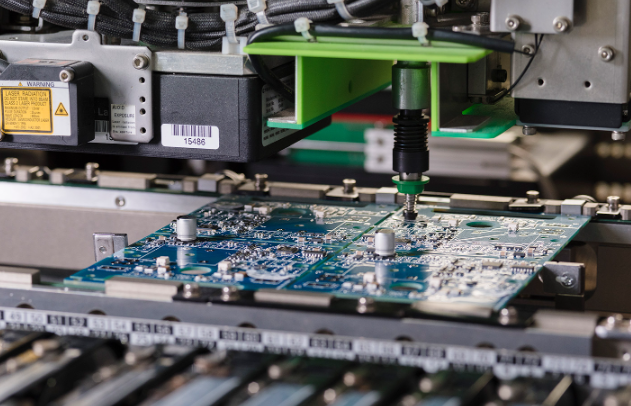
- Use advanced automated SMT assembly lines with ±0.03mm positioning accuracy, match professional X-ray detection equipment to inspect BGA and other complex components. Our R&D team optimizes soldering processes (±1℃ reflow soldering precision) to meet micron-level requirements of AI-driven and high-end devices.
- Assign industry-specific engineers (medical, aerospace, industrial control), conduct 1-on-1 demand communication to customize processes, materials and testing standards. Integrate one-stop service from design optimization to final assembly to fully match client-specific needs.
- Provide end-to-end METI-compliant documentation support, including document preparation, review and update. Our professional team ensures all documents meet relevant local regulations, saving clients time and energy in documentation management.
Why Choose EBest for PCB Assembly in Japan?
Reasons why choose EBest for PCB assembly in Japan:
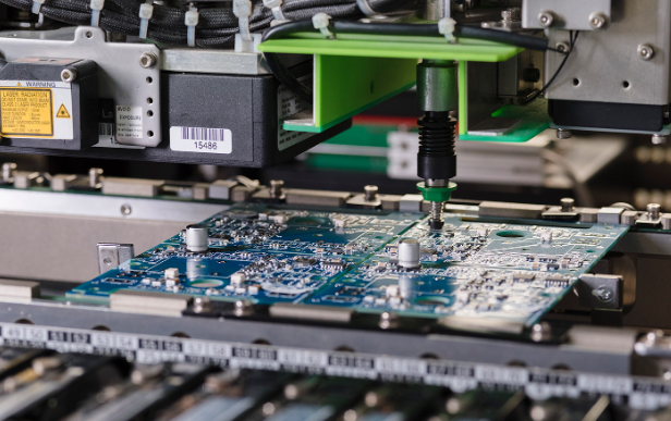
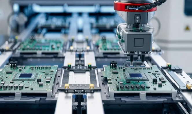
- Advanced MES System: We equip a professional MES system for PCB assembly in Japan, realizing full-process intelligent management and product traceability, which helps you track every production link, reduce quality risks, and ensure product consistency and traceability.
- One-Stop PCBA Solutions Service: We provide full-turnkey one-stop PCB assembly services for clients in Japan, covering PCB production, component sourcing, SMT/DIP assembly, functional testing and final packaging, saving you time and costs of cooperating with multiple suppliers.
- Authoritative Quality Certifications: We hold AS9100D (aerospace industry), ISO 13485:2016 (medical industry), IATF 16949 (automotive industry) and ISO 9001:2015 certifications, ensuring our PCB assembly in Japan fully meets the strict quality requirements of various industries.
- Stable and Reliable Component Supply: We have a robust global supply chain, ensuring stable access to genuine, high-quality electronic components (SMD, BGA, QFN, QFP) for PCB assembly in Japan, avoiding project delays caused by component shortages .
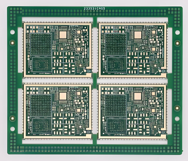
- High Production Capacity & Efficiency: With a monthly production capacity of 260,000 square feet (28,900 square meters) and automated production lines, we can efficiently handle both high-volume and low-volume/prototype PCB assembly in Japan, shortening your delivery cycle.
- Industry-Specific Customization: We provide customized PCB assembly in Japan solutions for medical, aerospace, and industrial equipment industries, tailoring services to meet the unique technical and compliance needs of your industry.
- Strict Quality Control: We implement 100% full inspection before delivery, adopt A+ grade materials, and follow IPC-A-610J CLASS III acceptance standards, ensuring the pass rate of PCB assembly in Japan reaches 99% or above.
- Professional R&D Support: We invest heavily in R&D to keep pace with Japan’s electronic manufacturing trends, providing technical support for complex high-precision PCB assembly, helping you realize product innovation and upgrading.
- Comprehensive After-Sales Service: We offer professional after-sales support for PCB assembly in Japan, including technical consultation, troubleshooting and maintenance guidance, solving your worries after order delivery.
What Services Does EBest Offer for PCB Assembly in Japan?
Core PCB Assembly Services:
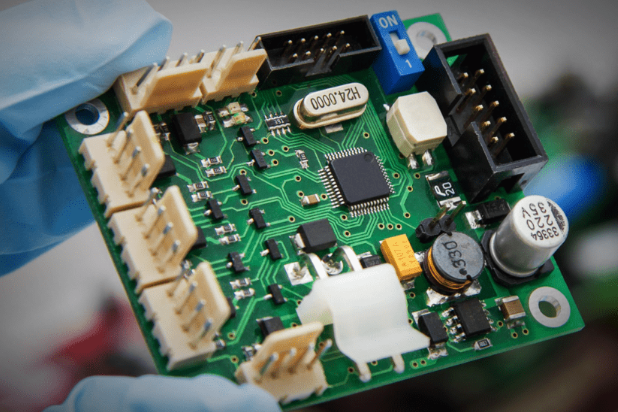
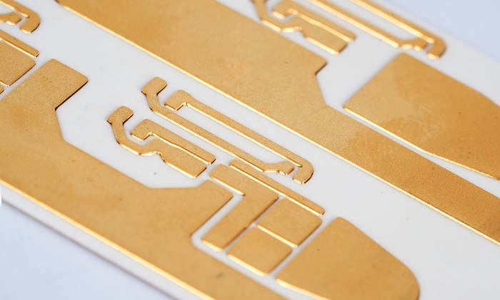
- BGA Assembly Service: High-precision PCB assembly for complex BGA components, tailored for advanced electronic devices in Japan. Our micron-level accuracy ensures stable performance, perfectly suited for AI-driven and high-tech products dominating Japan’s market.
- Through-Hole Assembly: Reliable through-hole component assembly for PCB assembly in Japan, delivering strong connectivity and long-term durability. Ideal for industrial equipment and rugged electronic devices requiring consistent performance in harsh environments.
- Flex PCB Assembly: Flexible PCB assembly solutions for compact, high-performance devices—perfect for Japan’s electronics industry, where miniaturization and portability are key demands for consumer and industrial products.
- Quick Turn PCB Assembly: Expedited PCB assembly in Japan for urgent orders, with 24-hour delivery for critical projects. Aligns with Japan’s fast-paced manufacturing cycle, supporting your “small-batch, quick-turn” production needs.
- Full Turnkey PCB Assembly: One-stop PCB assembly service for Japan’s clients, covering PCB production, component sourcing, SMT/DIP assembly, functional testing, and final packaging. Saves you time and costs by eliminating the need to coordinate multiple suppliers.
Value-Added Services:
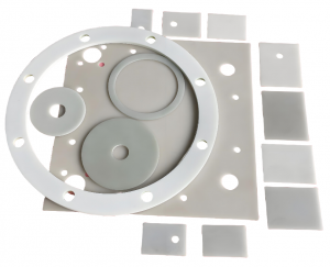
- Injection Molding: Comprehensive injection molding services to complement PCB assembly in Japan, including mold structure design, thread insert, pad printing, laser engraving, and final assembly, streamlining your production process.
- CNC Machining: High-precision CNC Milling and Turning with tight tolerances and anodizing options, designed to match the strict quality standards of PCB assembly in Japan for aerospace, medical, and industrial applications.
- Sheet Metal: Efficient sheet metal services for PCB assembly projects in Japan, featuring low material waste, flexible material selection, and multiple finishing options, reducing costs while ensuring compatibility with your PCB designs.
What Quality Certifications Does EBest Hold for PCB Assembly in Japan?
- IATF 16949: This certification ensures our PCB assembly in Japan fully complies with the strict quality and safety requirements of the automotive industry, supporting your automotive electronic component assembly needs.
- ISO 9001:2015: As a globally recognized quality management standard, it guarantees consistent quality control across all our PCB assembly services, delivering reliable results for every client in Japan.
- ISO 13485:2016: Tailored for the medical device industry, this certification ensures our PCB assembly in Japan meets the rigorous standards for medical equipment, prioritizing safety and zero-fault performance.
- AS9100D: Compliant with aerospace industry requirements, this certification is critical for high-reliability PCB assembly, making us a trusted partner for aerospace component assembly in Japan.
- RoHS & REACH: These environmental certifications ensure our PCB assembly in Japan meets both local and global environmental standards, restricting harmful substances and aligning with international new pollutant control requirements.
- UL: This safety certification guarantees the compliance and safety of electronic components used in our PCB assembly in Japan, reducing safety risks for your end products.

Our PCB Assembly Capabilities for Japan PCBA Orders
| Item | Capabilities |
| Placer Speed | 13,200,000 chips/day |
| Bare Board Size | 0.2 x 0.2 inches – 20 x 20 inches/ 22*47.5 inches |
| Minimum SMD Component | 01005 |
| Minimum BGA Pitch | 0.25mm |
| Maximum Components | 50*150mm |
| Assembly Type | SMT, THT, Mixed assembly |
| Component Package | Reels, Cut Tape, Tube, Tray, Loose Parts |
| Lead Time | 1 – 5 days |
Case Studies: Industrial Control PCB Prototyping in Japan
Custom Rigid-Flex PCB Assembly Project for Japanese Industrial Automation Client
Project Background: Our client is a leading Japanese industrial automation manufacturer specializing in smart factory control systems. Amid Japan’s booming industrial automation demand and equipment upgrades, their existing PCB assemblies had frequent signal interference, causing 8-10 monthly malfunctions, reducing production efficiency by 18% and increasing maintenance costs significantly.
Project Requirements:
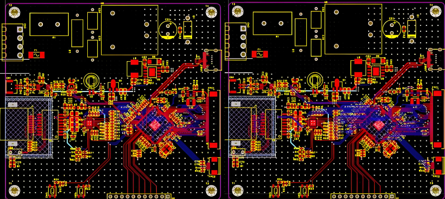
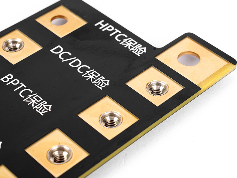
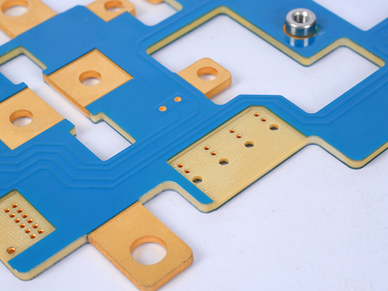
- Produce custom rigid-flex PCB assembly in Japan for control modules: 1.2mm thickness, 12 layers, 860+ components (SMD, BGA, through-hole).
- Withstand harsh industrial conditions: -40℃ to 85℃ operating temperature, 10-2000Hz vibration resistance, 95% humidity resistance (non-condensing).
- Comply with ISO 9001:2015, IATF 16949, and Japan’s METI industrial control standards.
- Deliver 5,000 units in 25 business days; prototype approval within 5 days.
- Guarantee ≥99.8% pass rate and ≥80,000-hour service life.
Project Difficulties:
- High precision: 0.5mm pitch BGA components require ±0.03mm assembly accuracy; rigid-flex connection prone to poor soldering and signal loss.
- Environmental adaptability: Strict material/soldering requirements to resist temperature cycles and industrial vibration.
- Tight timeline: 25-day delivery for 5,000 units plus 5-day prototype approval requires efficient scheduling.
- Component supply: High-temperature resistant components were in tight supply amid Japan’s industrial equipment boom.
Solutions
- Precision assembly: Used automated lines + MES system for full traceability; ±1℃ reflow soldering precision to ensure BGA soldering quality.
- Material optimization: Selected A+ grade FR-4+PI rigid-flex substrates and IPC-CC-830 conformal coating; 100+ environmental tests to verify performance.
- Efficient scheduling: Allocated dedicated lines (260,000 sq.ft/month capacity); 15% assembly time reduction via one-stop service.
- Stable supply: Locked 100% of required components in advance with 5% spares to avoid delays.
- Quality control: 100% AOI + X-ray inspection; 5% functional testing to ensure compliance.
Output Results
- Delivery: 5,000 units delivered 2 days early (23 business days); prototype approved in 4 days.
- Quality: 99.92% pass rate, exceeding the 99.8% requirement; no signal interference or soldering defects.
- Performance: Client’s monthly malfunctions dropped to 0-1; production efficiency improved by 28%.
- Compliance: Passed METI inspection and ISO 9001/IATF 16949 audits.
- Longevity: 85,000-hour service life, exceeding the 80,000-hour requirement.
FAQs About PCB Assembly in Japan
Q1: How long does EBest take for PCB assembly in Japan?
A1: Standard orders take 3-7 business days, while our quick turn service delivers urgent PCB assembly in Japan within 24 hours. Lead times are tailored to order volume and complexity.
Q2: Does EBest provide component sourcing for PCB assembly in Japan?
A2: Yes, we have a stable supply chain for all electronic components (SMD, BGA, QFN, QFP, etc.) for PCB assembly in Japan, ensuring genuine, high-quality parts with full traceability.
Q3: Is EBest’s PCB assembly in Japan compliant with RoHS and REACH?
A3: Absolutely. All our PCB assembly in Japan meets RoHS and REACH requirements, using lead-free materials and processes to ensure environmental compliance.
Q4: Can EBest produce prototype PCB assembly in Japan?
A4: Yes, we offer prototype PCB assembly in Japan for low-volume production, with customization options for special substrates or materials to support product development.
Q5: How does EBest ensure quality for PCB assembly in Japan?
A5: We implement 100% full inspection before delivery, use A+ grade materials, and follow strict quality control processes aligned with our ISO and industry-specific certifications.