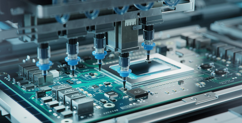
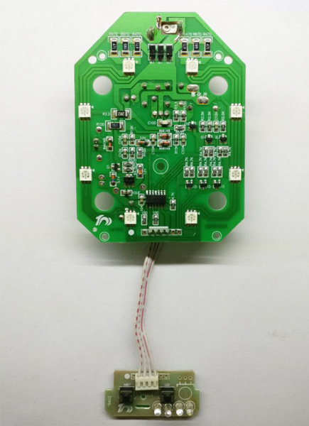
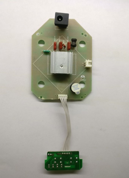
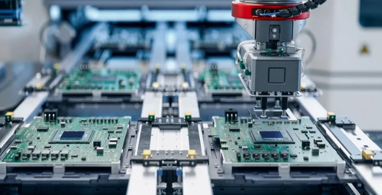
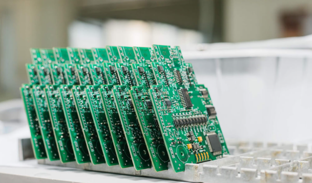
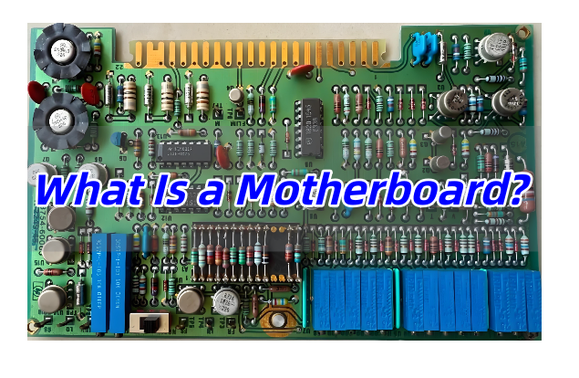
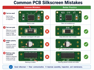
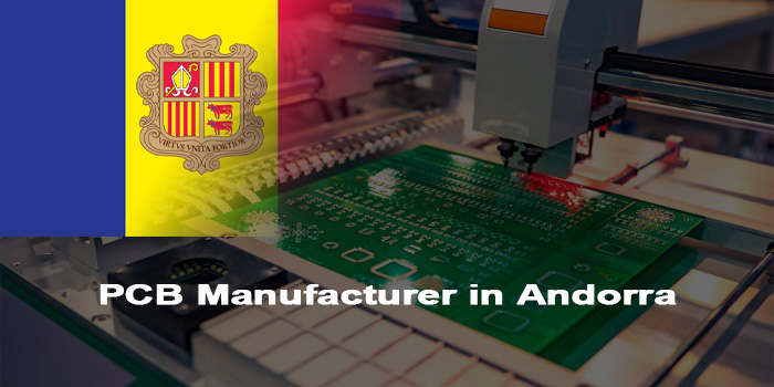
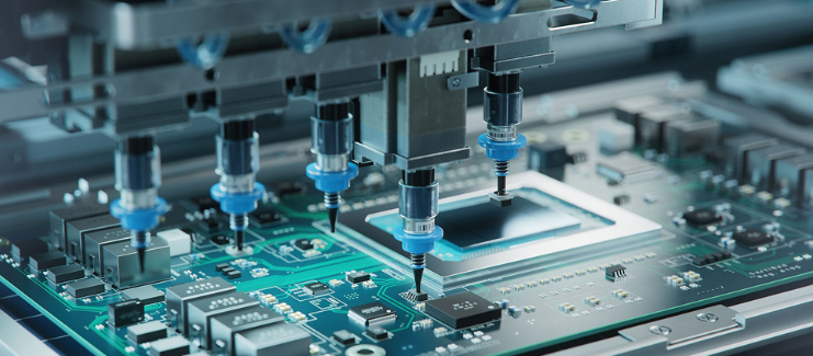
Andorra’s PCB manufacturing sector combines European quality standards with flexible production capabilities, making it a sought-after destination for precision electronic components. A PCB manufacturer in Andorra typically specializes in customized solutions for various industries, from automotive to medical electronics. Whether you need small-batch prototypes or mass production, partnering with a reputable PCB manufacturer in Andorra ensures compliance with international regulations and consistent product quality. This guide breaks down key aspects of Andorra PCB manufacturing, helping you navigate the market and select the right partner.
Top PCB Manufacturer in Andorra
| Company Name | Main Business | Core Advantages | Process Capability | Lead Time |
| EBest Circuit Co., Limited | Rigid-flex PCB, multi-layer flex PCB, special FPC, PCB assembly | 19 years experience, UL/ISO13485/RoHS certified, 10,000+ successful cases | 3-12 layer PCBs, min 3mil line width, immersion gold/OSP | Prototyping 3-7d, Mass 7-15d |
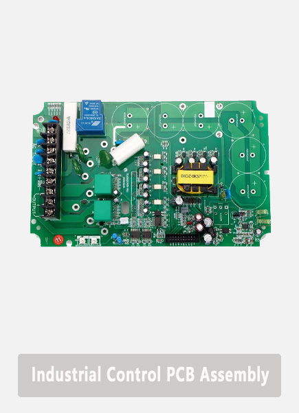
| Andorra Circuits S.L.U. | Single/double-layer rigid PCB, industrial control PCB | Local production base, ISO9001/ISO14001 certified, 99.5% pass rate | 2-6 layer PCBs, min 4mil spacing, aluminum base | Prototyping 4-6d, Mass 8-12d |
| La Massana PCB Factory | Medical device PCB, high-precision PCB | ISO13485 certified, sterile cleanroom, traceable materials | 2-8 layer PCBs, min 3mil line width, cleanroom production | Prototyping 6-8d, Mass 12-20d |
| Andorra High-Tech Circuits S.L. | High-frequency PCB, HDI PCB, aerospace-grade | AS9100 certified, PTFE material, strict quality inspection | 6-12 layer PCBs, blind/buried holes, 40GHz frequency | Prototyping 7-10d, Mass 15-25d |
| Andorra Green Electronics S.A. | Halogen-free PCB, eco-friendly PCB | ISO14001 certified, carbon-neutral, green supply chain | 2-6 layer PCBs, halogen-free substrates, lead-free | Prototyping 5-7d, Mass 9-14d |
| Andorra PCB Assembly Co. | Turnkey assembly, component sourcing | UL certified components, 99.2% pass rate | 1-12 layer assembly, SMT/through-hole, functional testing | Assembly 5-10d (volume-dependent) |
How to Select A Reliable Andorra PCB Manufacturing Company?
Selection Guide to Andorra PCB Manufacturing Company:
- Certification & Compliance Focus: Prioritize manufacturers with industry-specific certifications like ISO13485 (medical), IATF16949 (automotive), or AS9100 (aerospace). Verify compliance with RoHS/REACH for environmental standards and UL certification for safety-critical applications.
- Process Capability Match: Assess layer capacity (e.g., 6-12 layer for high-density designs), minimum line width/spacing (3mil/3mil for advanced signal integrity), and copper thickness (0.5-4oz for power-heavy applications). Confirm support for specialized processes like blind/buried vias or impedance control (±5% for high-frequency circuits).
- Local Production & Response Time: Identify manufacturers with physical facilities in Andorra to ensure rapid prototyping (3-7 days) and mass production lead times (7-15 days). Local supply chain integration reduces logistics delays and customs risks.
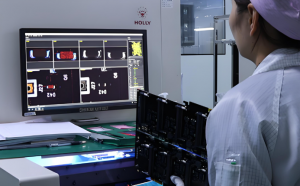
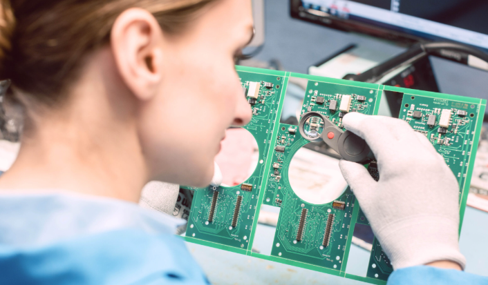
- Quality Control Systems: Look for 100% AOI (Automated Optical Inspection) or X-ray inspection capabilities. Check test pass rates (≥99.5% for reliability) and traceability systems for material origins. Cleanroom production (ISO Class 7 or higher) is critical for medical/automotive applications.
- Eco-Conscious Practices: Evaluate carbon-neutral production claims, halogen-free substrate options, and lead-free surface treatments (e.g., immersion silver/ENIG). Green supply chain management reduces environmental impact and aligns with global sustainability trends.
- Case Experience & Scalability: Review portfolio of successful projects (e.g., 10,000+ cases for mature processes). Confirm capability to scale from small-batch prototypes (1-10 units) to volume production (thousands of units) without quality degradation.
- Technical Support & Transparency: Ensure 24-hour technical assistance for design adjustments and DFM (Design for Manufacturing) feedback. Transparent communication about capability limits (e.g., minimum aperture 0.2mm) prevents misalignment during production.
What Quality Certification Should PCB Manufacturers in Andorra Have?
Quality Certification for PCB Manufacturer in Andorra:
- ISO 9001: Ensuring consistent production processes and product quality across all batches.
- RoHS: Mandatory for European markets, restricting hazardous substances in Andorra PCB manufacturing to meet environmental regulations.
- UL Certification: Covering PCB substrate flammability (UL 94) and overall reliability (UL 796).
- IPC-A-600: Industry-specific standard for PCB acceptance, guaranteeing compliance with electronic manufacturing best practices.
- ISO 14001: Environmental management certification, essential for sustainable Andorra PCB plant operations and regulatory compliance.
Production Capability of Andorra PCB Manufacturing Company
| Capability Parameter | General Range | High-End Range |
| Number of Layers | 1-8 layers | 2-12 layers |
| Minimum Line Width/Spacing | 4/4 mil | 3/3 mil |
| Minimum Aperture | 0.2 mm | 0.1 mm |
| Copper Thickness | 0.5 oz – 2 oz | 0.5 oz – 4 oz |
| Board Thickness | 0.2 mm – 3.0 mm | 0.2 mm – 8.0 mm |
| Surface Treatment | Spray tin, OSP, immersion gold | Immersion silver, hard gold, ENIG |
| Impedance Control | ±10% | ±5% |
How to Evaluate the Delivery Capability of PCB Manufacturer in Andorra?
Evaluation Guide to Delivery Capability of PCB Manufacturer in Andorra:
- Verify 12-month on-time delivery rate, taking ≥95% as baseline. This exceeds the global PCB industry average of 88% ,and prioritize manufacturers with verifiable batch delivery data to avoid occasional high-rate outliers.
- Assess spare capacity at Andorra PCB factory, ensuring ≥20% reserve. This capacity can cope with peak urgent orders, and prefer factories with flexible production lines to adapt to order fluctuations.
- Evaluate supply chain stability, prioritizing ≥60% local raw material sourcing. Amid rising copper and substrate costs ,local sourcing cuts 30% of supply disruption risks and shortens procurement cycles.
- Check urgent prototype response, requiring 2-3 day turnaround. Ensure the factory maintains dedicated prototype lines and retains 100% AOI testing to avoid quality compromises for speed.
- Confirm real-time tracking systems that connect production nodes and shipping logistics. The system should send automatic alerts for delays over 4 hours to enable timely adjustments.
- Inspect packaging standards compliant with IPC-A-600. Adopt anti-static bags and moisture-proof vacuum packaging to control transit damage rate below 0.1%.
- Assess EU cross-border shipping experience. Verify complete documentation including RoHS, CE certificates and material declarations to ensure customs clearance time within 2 working days.
How to Evaluate Technical Capability of Andorra PCB Manufacturing Company?
Evaluation Guide to Technical Capability of Andorra PCB Manufacturing Company:
- Review past project cases: Prioritize Andorra PCB manufacturers with ≥50 complex project cases within the past two years, including HDI (accounting for 18% of global PCB demand) and rigid-flex PCBs, with a customer retention rate of ≥98% for such orders.
- Test prototype quality: Ensure prototype accuracy deviation ≤0.1 mil, consistency with design specifications ≥99.5%, and verify through three consecutive batches of samples to avoid accidental accuracy.
- Evaluate DFM support: Require ≥3 targeted optimization suggestions before production, which can reduce the trial production defect rate by ≥15% and shorten the mass production cycle by 7-10 days.
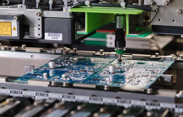
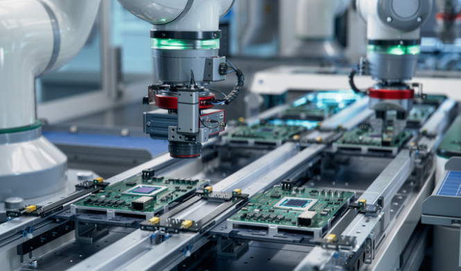
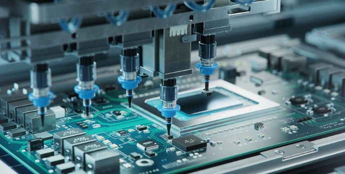
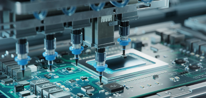
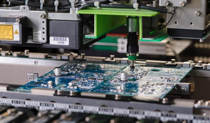
- Inspect production equipment: Confirm the availability of high-precision exposure machines and AOI inspection tools with accuracy ≥2μm, covering 100% surface defect detection, meeting advanced Andorra PCB manufacturing standards.
- Evaluate material quality control: Ensure raw materials come from the top 50 global suppliers, with a sampling rate of ≥10% per batch, and 100% compliance with certificate requirements, avoiding quality risks caused by inferior substrates.
- Check technical team response speed: Require a response rate of ≥98% within 8 hours for general inquiries and provide clear solutions for complex problems within 48 hours, with a response efficiency 30% higher than the industry average.
- Evaluate process innovation: Prioritize manufacturers that utilize ≥2 environmentally friendly or efficient technologies, increasing production efficiency by ≥20% and reducing environmental costs compared to traditional processes.
Future Challenges of PCB Manufacturer in Andorra
- Rising raw material costs, especially copper and substrate materials, squeezing profit margins.
- Stringent environmental regulations, requiring upgraded waste treatment for Andorra PCB manufacturing.
- Global competition from Asian manufacturers with lower production costs.
- Rapid technological upgrades, demanding continuous investment in HDI and high-frequency PCB capabilities.
- Skilled labor shortage, affecting production efficiency and technical innovation.
- Supply chain disruptions from international geopolitical factors.
- Increasing customization demands, requiring flexible production lines and shorter lead times.
FAQs of PCB Manufacturing in Andorra
Q1: How to resolve line oxidation and copper exposure in Andorra PCB production?
A1: We control storage humidity at ≤ 40% and use high-quality solder mask ink with 100% post-printing inspection. Our PCB manufacturer in Andorra applies anti-oxidation treatment to all prototypes and mass production runs ensuring no copper exposure.
Q2: Why do PCB prototypes have inconsistent impedance values and how to fix it?
A2: Inconsistency comes from imprecise line etching or improper substrate selection. We use impedance simulation software pre-production and control etching parameters with ±2% accuracy. As a professional Andorra PCB manufacturer, we guarantee ±5% impedance tolerance for high-precision orders.
Q3: How to avoid board warping during multi-layer PCB production in Andorra?
A3: Warping is caused by uneven lamination pressure. Our Andorra PCB plant uses precision lamination equipment with temperature controlled at ±1℃ and pressure at ±0.5kg/cm² plus pre-testing of substrate shrinkage rate. We ensure board warpage ≤ 0.5% for all multi-layer boards.
Q4: What causes poor hole metallization and conductivity issues in Andorra PCB manufacturing?
A4: This results from incomplete hole cleaning or uneven copper plating. We implement a three step hole cleaning process and real time plating thickness monitoring. Our PCB Andorra manufacturer achieves 99.9% hole conductivity rate with 100% electrical testing.
Q5: How to shorten lead time for custom PCB prototypes in Andorra without compromising quality?
A5: We optimize production flow with dedicated prototype lines and 24 hour processing capability. Our Andorra PCB company delivers 3-5 layer prototypes in 2-3 days with full AOI and electrical testing.