





pcb traces are the copper paths that connect component pads, vias, connectors and test points. A useful trace design must satisfy fabrication limits, electrical clearance, current capacity and signal requirements.
This guide shows how to recognize a trace, select practical design rules and check a damaged route. It also includes our complete FR4 line width and spacing table for different copper weights.
What Are Traces on a PCB?
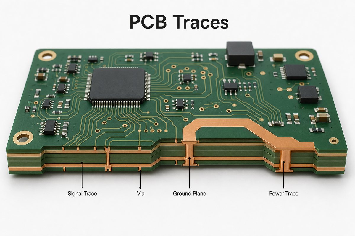
A PCB trace is a patterned copper conductor that carries a signal or supply current between two electrical nodes. On an outer layer, the trace usually appears as a narrow path beneath the solder mask. Its exposed ends become pads for soldering, probing or connection.
Four dimensions define the physical conductor:
- Trace width is the horizontal width of one copper path.
- Trace spacing is the copper-to-copper gap between neighboring features.
- Copper thickness is the vertical thickness of the conductor.
- Trace length is the routed distance between its endpoints.
Width and thickness determine the copper cross-section. Length then affects resistance, voltage drop and signal delay. This is why two traces that look similar may perform differently.
PCB Trace Material and Copper Thickness
PCB trace material is normally electrodeposited or rolled copper. The following table converts the most common nominal copper weights into thickness.
| Copper Weight | Nominal Thickness |
| 0.5 oz | Approximately 17 µm |
| 1 oz | Approximately 35 µm |
| 2 oz | Approximately 70 µm |
| 3 oz | Approximately 105 µm |
These figures describe nominal foil thickness, not a guaranteed finished measurement at every point. Outer-layer plating adds copper, while etching changes the sidewalls and finished width. The fabrication drawing should therefore state the required finished copper when that value controls current or impedance.
For FR4 boards, our standard range is 0.5–5 oz for inner copper and 1–5 oz for outer copper. Special processes extend both inner and outer copper to 20 oz. Heavier copper needs wider spacing because deeper etching makes fine conductors harder to hold.
Types of PCB Traces
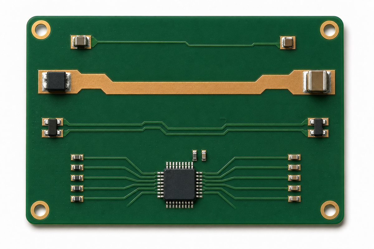
Types of PCB traces are separated by electrical function, because each function creates a different design priority. The same minimum fabrication rule should not be used blindly for every net.
| Trace Type | Design Priority | Primary Check |
| Ordinary signal trace | Reliable connection and practical routing | Width, spacing and continuity |
| Power trace | Low resistance and controlled heating | Current, voltage drop and neck-down width |
| Differential pair | Matched propagation and coupling | Pair width, gap and length mismatch |
| Controlled-impedance trace | Target transmission impedance | Stackup, width and reference plane |
| RF trace | Low discontinuity and predictable return current | Geometry, transitions and ground reference |
A route can belong to more than one group. A high-speed differential pair is also a controlled-impedance structure, so changing its width or pair gap after routing changes the electrical result.
How Are PCB Traces Made?
PCB traces are made by transferring the circuit image to copper-clad laminate and etching away the unwanted copper. The finished geometry comes from the artwork, copper thickness and process compensation used by the fabricator.
- Clean and coat the copper. A photosensitive resist is applied to the copper surface.
- Image the circuit. Film exposure or laser direct imaging defines the tracks, pads and clearances.
- Develop and etch. The process protects wanted copper and removes the open areas.
- Inspect the pattern. AOI compares the etched conductors with the production data and finds opens, shorts or damaged features.
- Build and test the board. Inner layers are laminated, outer layers are processed, and electrical testing verifies continuity and isolation.
Etching does not produce perfectly vertical copper walls. Thick copper needs more lateral etch compensation, which explains why the minimum line and space increase as copper weight rises.
What Are the Differences Between PCB Traces and Vias?
PCB traces carry a connection across one copper layer, while vias carry it vertically between layers. A trace is an etched horizontal conductor; a via is a plated hole with pads on the layers it connects.
The two features work together when a net changes layers. We support 0.10 mm laser blind or buried vias. Our minimum finished mechanical hole is 0.20 mm for standard processing and 0.15 mm for special processing. The maximum through-hole aspect ratio is 8:1 standard and 10:1 special.
One small via should not become the narrowest point in a high-current path. Use enough via copper for the required current and place return vias near high-speed layer transitions. A signal via without a nearby return path forces return current to take a longer route, increasing loop area and discontinuity.
How to Read PCB Traces?
To read PCB traces, begin at a known pad and follow the same copper path until it reaches another pad, a via or a plane. Work on an unpowered board and use the schematic or PCB files whenever they are available.
- Identify the component reference and pin number.
- Follow the visible route under good lighting or magnification.
- Mark every via where the route may change layers.
- Use continuity mode to confirm suspected endpoints.
- Compare the result with the schematic net instead of relying only on appearance.
Ground pours and internal planes can make many points appear connected. Zero-ohm resistors can also look like ordinary components while acting as routing links. Recording each confirmed point prevents repeated probing and accidental pad damage.
PCB Trace Design Rules
PCB trace design rules should convert the stackup and fabrication capability into constraints that the layout software can check. A useful rule set separates ordinary signals, power nets, controlled-impedance routes and high-voltage circuits.
Set these values before detailed routing:
- Minimum trace width and copper spacing for each layer and copper weight.
- Electrical clearance based on working voltage and the applicable safety requirement.
- Via diameter, finished hole, annular ring and allowed via structures.
- Differential-pair width, gap and permitted length mismatch.
- Controlled-impedance geometry from the confirmed production stackup.
- Wider neck-down limits for pads, connectors and high-current transitions.
A PCB design rule check finds violations of the entered constraints. It cannot correct a wrong rule value, so DRC should follow stackup and capability confirmation rather than replace it.
How Wide Should PCB Traces Be?
PCB trace width should stay at or above the line/space value for the selected copper weight, then increase where current, voltage drop or impedance requires it. A 4/4 mil capability means a minimum 4 mil line beside a minimum 4 mil copper gap.
The table below shows our complete FR4 line width and spacing data. Standard values are the preferred production limits. Special values require stackup and engineering review before release.
| Layer | Copper Weight | Standard Line/Space | Special Line/Space |
| Inner | 0.5 oz | 4/4 mil | 3/3 mil |
| Inner | 1 oz | 4/4 mil | 3/3 mil |
| Inner | 2 oz | 6/6 mil | 5/5 mil |
| Inner | 3 oz | 10/12 mil | 8/8 mil |
| Inner | 4 oz | 12/16 mil | 10/10 mil |
| Inner | 5 oz | 16/20 mil | 10/14 mil |
| Inner | 6 oz | 22/26 mil | 14/16 mil |
| Inner | 10 oz | 36/40 mil | 28/34 mil |
| Inner | 20 oz | 74/90 mil | 60/80 mil |
| Outer | 1 oz | 4/4 mil | 3/3 mil |
| Outer | 1.5 oz | 6/6 mil | 4/4 mil |
| Outer | 2 oz | 8/8 mil | 6/6 mil |
| Outer | 3 oz | 12/12 mil | 9/9 mil |
| Outer | 4 oz | 16/16 mil | 12/12 mil |
| Outer | 5 oz | 20/20 mil | 15/15 mil |
| Outer | 6 oz | 26/26 mil | 20/20 mil |
| Outer | 10 oz | 40/40 mil | 32/32 mil |
| Outer | 20 oz | 90/90 mil | 70/70 mil |
Do not choose 3/3 mil merely because it appears in the special column. Wider spacing improves process margin, especially on heavy copper. Use the smallest value only where routing density makes it necessary.
How to Calculate Current Capacity of PCB Traces?
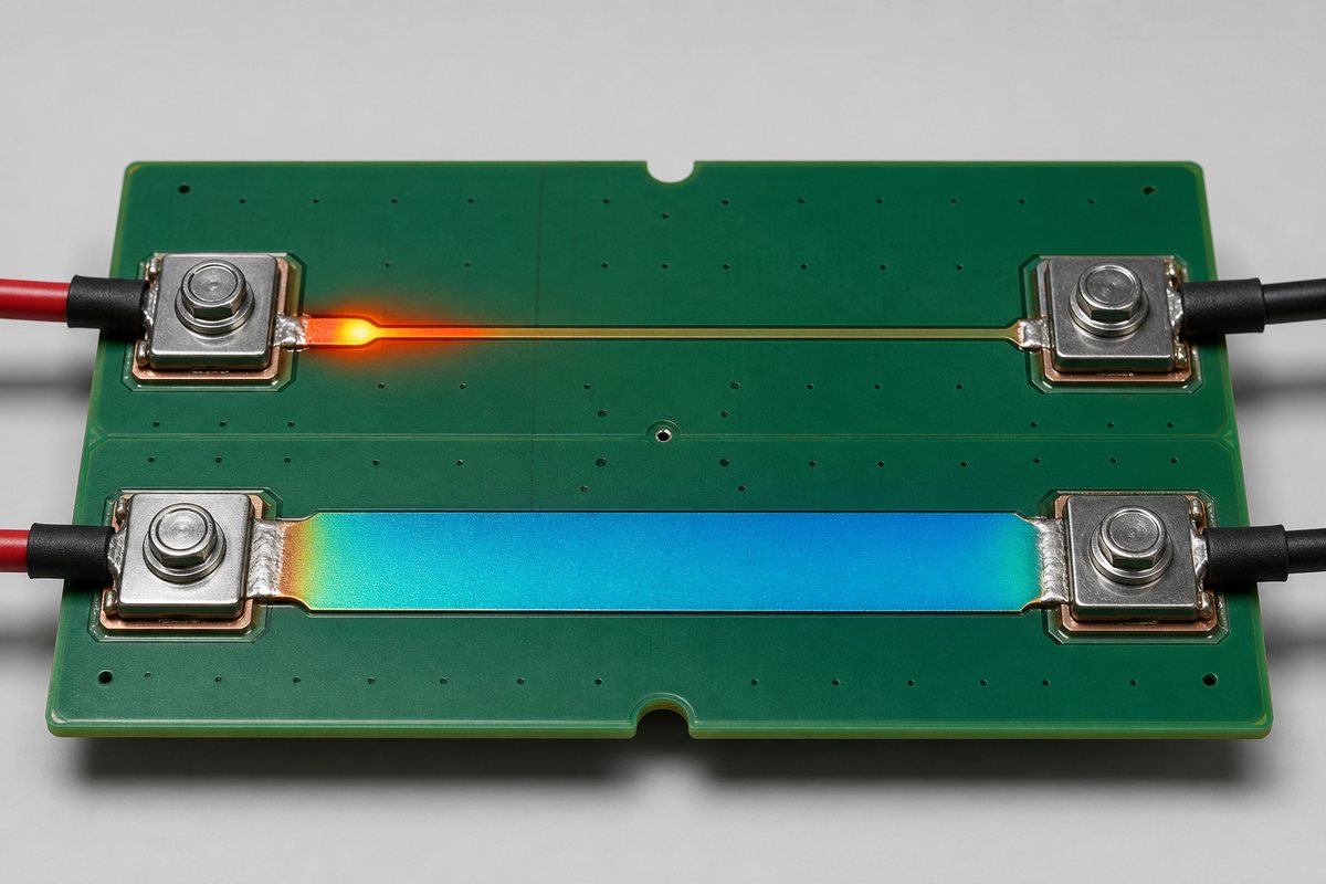
The current capacity of PCB traces is set by allowable temperature rise, not by a single current-per-mil rule. Use the actual copper thickness, layer position and available cooling when selecting the width.
Start with IPC-2152 conductor-sizing data, then check resistance with R = ρL/(w × t). For example, an ideal 100 mm long, 10 mil wide trace in 35 µm copper is about 0.19 Ω at room temperature. At 1 A, that creates about 0.19 V drop and 0.19 W of heat before temperature and process effects are considered.
A complete sizing check follows this order:
- Define continuous current, peak current and duty cycle.
- Select the allowed trace temperature rise.
- Choose width from the correct internal or external conductor condition.
- Calculate voltage drop along the complete path.
- Verify the prototype at the narrowest and hottest locations.
High current PCB traces should use the shortest practical route and enough copper cross-section to control both heat and voltage drop. Increasing width is usually the first step; heavier copper or parallel layers may be needed when board space is limited.
Inspect the entire current path rather than its widest area. The effective bottleneck may be:
- A narrow connection entering a component pad.
- A thermal relief with thin spokes.
- A single via between large copper pours.
- A connector pin or fuse footprint with limited copper.
The relationship between copper thickness and circuit width also changes manufacturability. Confirm heavy-copper spacing before final routing, not after the layout is crowded.
Why Are PCB Traces 45 Degrees?
PCB traces commonly use 45-degree bends because they produce compact routes without the sharp inside corner of a square turn. They are easy to route consistently and work well for most ordinary digital and analog layouts.
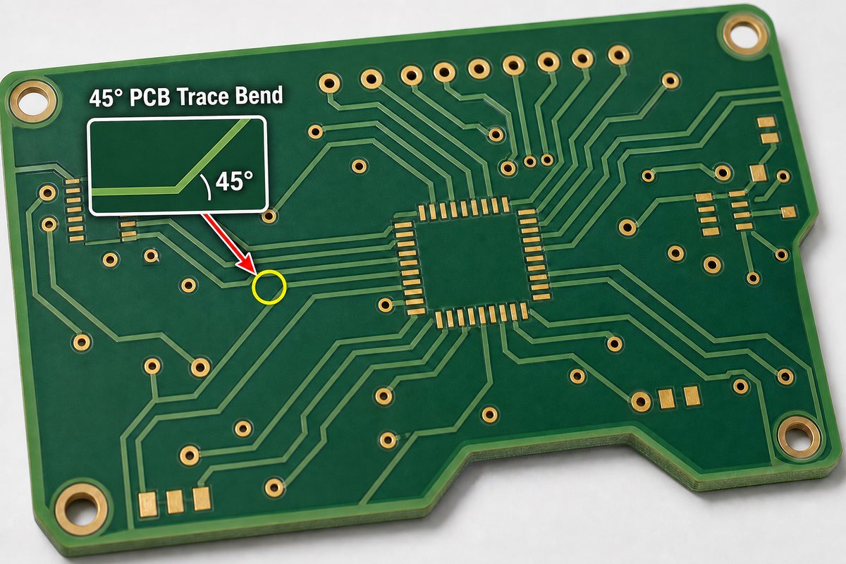
A 90-degree bend does not automatically cause an EMI failure. High-speed performance depends more on impedance continuity and the return path than on the visual angle alone. RF routes may use arcs or mitered bends after calculation, while low-speed traces rarely need that extra geometry.
How to Repair PCB Traces?
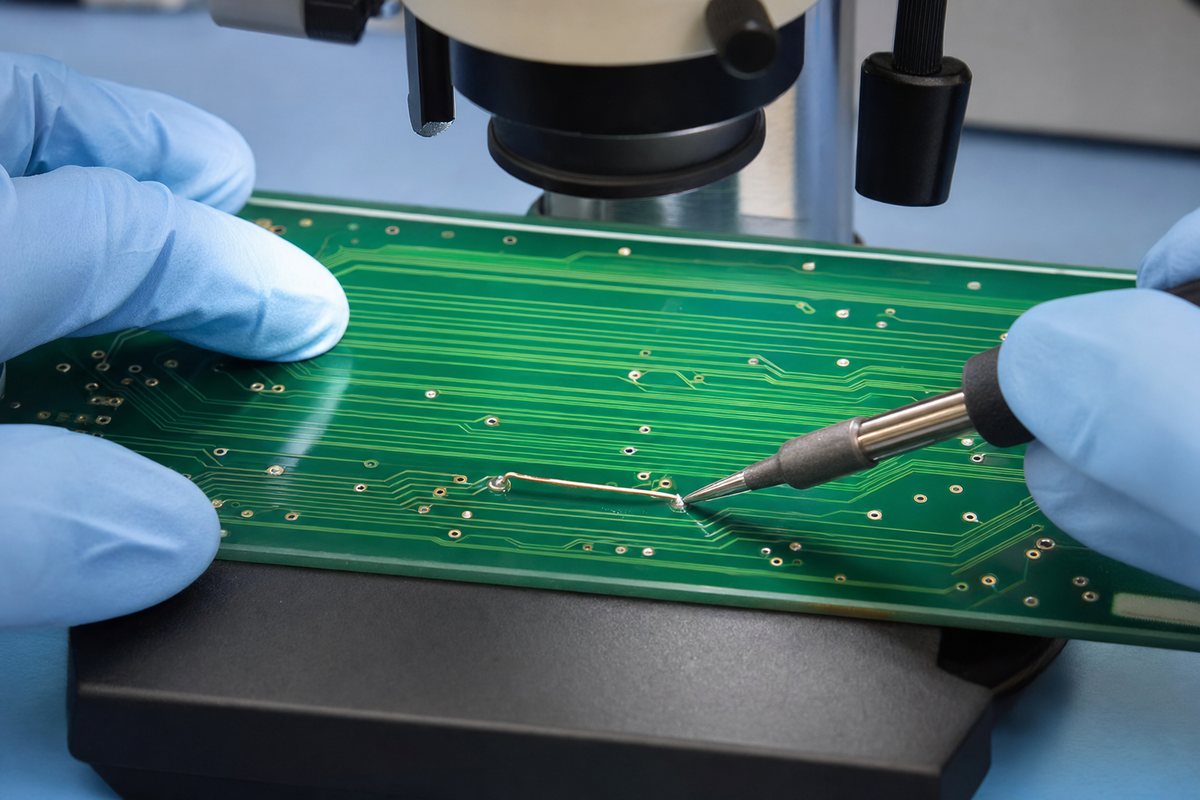
To repair PCB traces, remove the failed copper from the load path and bridge the break between two sound conductor points. The board must remain unpowered until continuity and isolation checks are complete.
- Find the original fault before repairing the visible damage.
- Remove loose or carbonized material and clean the area.
- Expose a short section of clean copper on both sides of the break.
- Tin the copper and install a conductor sized for the circuit current.
- Anchor the conductor so vibration cannot pull on the repaired pads.
- Measure continuity to the endpoints and isolation from adjacent nets.
Stop the repair when damage enters a plated hole, internal layer or controlled-impedance route that cannot be verified. Burned laminate must also be removed or professionally evaluated because carbonized material can remain electrically conductive.
FAQ About PCB Traces
Are PCB traces copper or gold?
PCB traces are copper. ENIG or another finish may cover exposed pads, but the thin surface finish protects the underlying copper rather than replacing it.
Can PCB traces cross?
Two unrelated traces cannot cross on the same copper layer. One route must change layers through vias, use a jumper or take a different path.
What is the difference between a PCB trace and a track?
Trace and track normally describe the same copper conductor. The preferred word depends on the region, company or PCB design software.
Can a PCB trace run under a component?
Yes, if the trace maintains the required clearance and does not interfere with pads or exposed metal. Sensitive analog and RF layouts may need additional restrictions.
What happens when a PCB trace is too narrow?
A narrow power trace has more resistance, voltage drop and heating. A narrow controlled-impedance trace also changes impedance, so the result depends on the net function.
How do you measure PCB trace width?
Read the nominal width from the PCB data and inspect the finished conductor with calibrated optical equipment. Manufacturing acceptance must use the agreed tolerance and inspection method.
What causes a PCB trace to burn?
Overcurrent, a short circuit or a high-resistance connection can overheat a trace. The fault must be corrected before replacing the damaged conductor.
Can a repaired trace carry the original current?
Only when the repair restores enough conductor cross-section and secure attachment. A continuity reading alone does not prove that the repair can carry the original load.
How Can EBest Circuit Support Your PCB Trace Requirements?
At EBest Circuit, we review FR4 trace geometry against the selected copper weight, layer structure, via requirements and production process. We keep standard and special limits separate so each project is evaluated against the correct manufacturing route.
Send your Gerber or ODB++ files, stackup, finished copper requirements, current information and impedance targets to sales@bestpcbs.com. Our engineering team will review the data and provide manufacturing feedback with the quotation.







