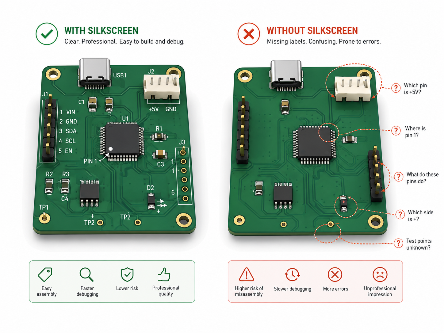
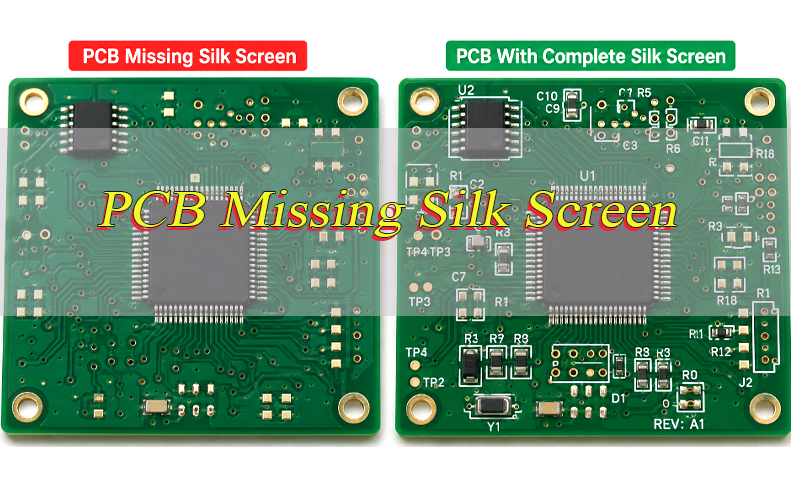
PCB missing silk screen means the printed text, reference designators, polarity marks, connector labels or board identification marks are absent, incomplete or unreadable on the finished PCB. The board may still pass electrical testing, but missing markings can create real risks during assembly, inspection, repair and batch traceability.
This guide explains why PCB missing silk screen happens, how Gerber files and EDA settings cause missing legend layers, how to check the problem before production, and how DFM review helps prevent repeated manufacturing defects. It is written for PCB designers, purchasing teams, quality inspectors and companies preparing prototype or batch PCB production.
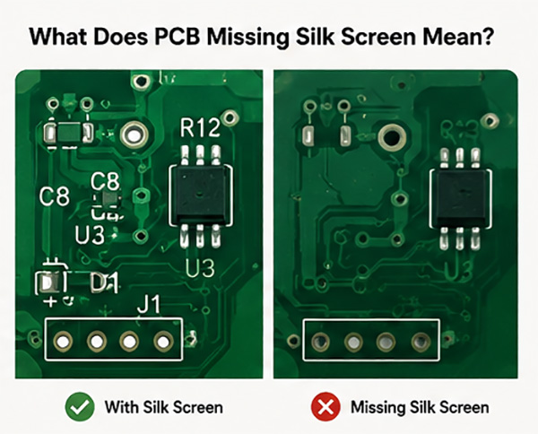
What Is PCB Missing Silk Screen?
PCB missing silk screen is a PCB marking defect where expected text, symbols, outlines or reference labels are not visible on the final board. These markings are normally printed on the solder mask surface and help identify components, test points, polarity, connectors, revision codes and warning labels.
In PCB manufacturing, silkscreen is also called the legend layer or overlay layer. It does not normally carry electrical current, but it provides important production information. When the top or bottom legend layer is missing, the PCB can become harder to assemble and inspect.
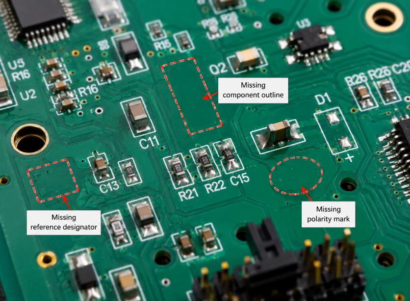
PCB missing silk screen may appear as a completely blank board, missing reference designators, broken text, shifted labels, faint ink or removed markings near solder pads. The cause may come from CAD settings, Gerber export, CAM processing, printing control or quality inspection failure.
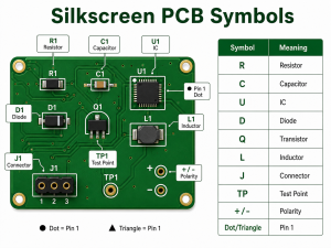
Common missing items include:
- Reference designators: R1, C5, U3, D2 and other component IDs.
- Polarity marks: diode, LED, capacitor, IC pin 1 and connector orientation.
- Test labels: TP1, GND, VCC, UART, SWD or programming port labels.
- Board information: part number, revision, date code, logo and batch mark.
- Warning marks: high voltage, fuse rating, connector direction or safety notes.
Can a PCB Function Without Silkscreen?
Yes, a PCB can function without silkscreen if the copper traces, vias, solder mask, plating, components and solder joints are correct. Silkscreen is not part of the electrical circuit, so its absence does not automatically make the PCB electrically defective.
However, PCB missing silk screen can still create production and maintenance risks. Operators may install polarized parts in the wrong direction, confuse connectors, misread test points or spend extra time checking assembly drawings. For one-off prototypes, this may be manageable. For batch production, it can increase rework and inspection pressure.
A PCB without silkscreen is more acceptable when the board is very simple, the component count is low and the assembly file is clear. For dense SMT boards, industrial controllers, power modules, communication boards or medical-related PCB assemblies, readable silkscreen is strongly recommended.
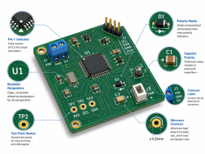
Why Does PCB Silkscreen Matter for Assembly, Testing and Repair?
PCB silkscreen matters because it links the physical board to the BOM, assembly drawing, test procedure and repair process. It helps people quickly understand what each component, connector and test point does.
During assembly, reference designators help operators match components with the BOM and pick-and-place file. Polarity marks reduce the risk of reversed LEDs, diodes, electrolytic capacitors and ICs. Connector labels help avoid cable direction mistakes during box build or system integration.
During testing and repair, clear labels help technicians find failed circuits faster. They do not need to check PCB layout files repeatedly just to locate one test point or component. For global supply projects, silkscreen also supports communication between the PCB factory, PCBA team, buyer and after-sales repair team.
Key value includes:
- Faster assembly: operators identify components more quickly.
- Lower polarity risk: direction-sensitive parts are easier to place correctly.
- Simpler testing: test points and programming pins are easier to locate.
- Better repair: technicians can trace failures with less file checking.
- Cleaner traceability: revisions, date codes and batch marks are easier to manage.
What Are the Common Causes of Missing Silkscreen on Printed Circuit Boards?
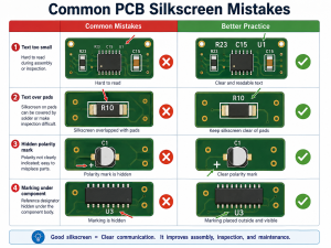
The most common causes of PCB missing silk screen are missing Gerber legend layers, hidden CAD text, wrong layer mapping, silkscreen over pads, small text size and CAM cleanup. The issue often starts before the PCB enters production.
On the design side, reference designators may be hidden in the PCB editor, placed on a fabrication layer instead of a silkscreen layer, or removed during footprint cleanup. Some designers also move text outside the board outline or forget to enable bottom-side markings before export.
On the manufacturing side, the factory may clip markings that overlap solder pads, exposed copper, vias or solder mask openings. This is done to prevent ink contamination on solderable surfaces. If the text is too small, too thin or too close to copper, it may become broken, faint or removed during CAM review.
Common causes include:
- Missing legend file: top or bottom silkscreen Gerber was not exported.
- Hidden reference designators: text is visible in CAD settings but not plotted.
- Wrong layer assignment: labels are placed on assembly or fabrication layers.
- Pad overlap: markings touch solder mask openings or exposed copper.
- Small text size: characters are below factory printing capability.
- CAM clipping: software removes text near pads, vias or board edges.
- Printing issue: ink, screen, alignment or curing control is unstable.
How Do Gerber Files Cause Missing Silkscreen Top or Bottom Layers?
Gerber files cause missing silkscreen top or bottom layers when the required overlay files are absent, empty, misnamed, mirrored or excluded from the export package. The final Gerber package is what the PCB factory uses for production.
For many PCB designs, the top silkscreen file is named GTO or top overlay, while the bottom silkscreen file is named GBO or bottom overlay. If either file is missing, the factory cannot print that side unless the customer provides corrected data. This is a common reason for PCB missing silk screen after export.
Gerber files missing silkscreen top layers are especially risky because most component reference designators and polarity marks are placed on the top side. Bottom legend errors may affect connector labels, test points, revision marks or assembly notes on double-sided boards.
| Check | Good Result | Warning Sign |
|---|---|---|
| Top legend | GTO or top overlay exists | File missing or empty |
| Bottom legend | GBO or bottom overlay exists | Layer not exported |
| Board outline | Aligned with all layers | Legend shifted or mirrored |
| Text content | Refdes visible | CAD shows text, Gerber does not |
| Polarity | Clear marks in Gerber | Marks only in assembly drawing |
| CAM preview | No critical clipping | Labels removed near pads |
Before release, always open the full Gerber package in an independent viewer. The PCB editor view is not enough because it may show design objects that were not exported.
Why Are PCB Reference Designators Missing After Export?
PCB reference designators are usually missing after export because the text fields are hidden, placed on the wrong layer, excluded from plotting or filtered by output settings. This problem is common in both prototype and batch PCB projects.
A reference designator may appear on the design screen but fail to appear in Gerber output. This happens when the footprint field is not assigned to the silkscreen layer, the plot option excludes component text, or the design uses assembly-layer labels instead of board legend labels.
PCB missing reference designators can also happen when text overlaps pads or vias. During CAM cleanup, the factory may remove or clip these markings to keep ink away from solderable areas. This protects solderability, but it may leave the board with missing component identification.
To avoid this problem:
- Check visibility: make sure reference designators are not hidden.
- Check layer: place refdes on top or bottom silkscreen, not only assembly layers.
- Check export settings: include component text in Gerber output.
- Check clearance: keep text away from pads, vias and exposed copper.
- Check Gerber viewer: confirm refdes appears in the final manufacturing files.
How to Identify PCB Missing Silk Screen Before Manufacturing?
The best way to identify missing PCB silkscreen before manufacturing is to inspect the exported Gerber files, not only the PCB design screen. The Gerber package is the real manufacturing data.
Open all copper, solder mask, drill, board outline and silkscreen layers in a Gerber viewer. Confirm that the top and bottom legend layers appear on the correct side. Then zoom into dense areas around ICs, connectors, diodes, LEDs, capacitors, test points and programming ports.
Next, compare the Gerber view with the BOM, assembly drawing and pick-and-place file. Check whether each critical component has a readable reference designator and whether polarity marks are still visible. For PCB missing silk screen prevention, this review should be completed before requesting a production quotation.
Important inspection points include:
- Layer completeness: top and bottom legend files are included.
- Side accuracy: top and bottom markings are not reversed.
- Text readability: letters remain clear after zooming out.
- Critical marks: polarity, pin 1 and connector labels are visible.
- Clearance: no text overlaps solder mask openings.
- Revision: board name, version and date code are correct.
- File consistency: Gerber, BOM and assembly drawing match each other.
How to Troubleshoot PCB Silk Screen Printing Problems?
PCB silk screen printing troubleshooting should start from Gerber data, then move to CAM editing, printing process and final inspection. This order avoids blaming production before confirming whether the marking existed in the manufacturing files.
- Check the final Gerber files
Open the exported Gerber package in an independent viewer. If the missing text does not appear in the silkscreen layer, the problem comes from CAD settings, hidden text or export configuration, not printing. - Confirm top and bottom legend layers
Check whether the top overlay and bottom overlay files are included. A missing GTO or GBO file can directly cause PCB missing silk screen on one side of the board. - Review CAM clipping records
If the text appears in Gerber but disappears on the PCB, check whether CAM removed markings near pads, vias, exposed copper or board edges. This is often done to protect solderability. - Inspect text size and stroke width
Very small characters may break during printing. Text that is too thin can become faint after curing, especially on dark solder mask or dense SMT areas. - Check ink, screen and alignment
Broken or blurred markings may come from blocked mesh, unstable ink viscosity, poor registration or weak printing pressure. These are process issues, not design issues. - Verify curing and adhesion
If markings fade after reflow, cleaning or handling, check ink curing, solder mask surface condition and cleaning chemistry. Poor adhesion can make silkscreen peel or disappear. - Compare with the approved sample
For repeat orders, compare the failed PCB with the golden sample. Repeated defects in the same location usually point to data or CAM rules. Random defects usually point to process control.
How to Fix KiCad Silkscreen Not Showing on PCB?
KiCad silkscreen not showing on PCB is usually caused by hidden fields, wrong layer placement or incomplete Gerber plot settings. The fix should be confirmed in the exported Gerber files, not only in the PCB editor view.
- Check reference designator visibility
Open the footprint properties and confirm that reference designators are visible. If the fields are hidden, they may not be plotted and can cause missing component markings. - Confirm the correct silkscreen layer
Printed top-side text should be on F.SilkS. Printed bottom-side text should be on B.SilkS. Text placed on Fab, Courtyard, User or Assembly layers will not automatically print on the PCB. - Move critical markings away from pads
Place polarity marks, pin 1 indicators and connector labels away from solder pads and exposed copper. If the markings overlap solder mask openings, the factory may remove them during CAM cleanup. - Enable silkscreen layers during plotting
In the Gerber plot settings, make sure front silkscreen and back silkscreen are selected. Missing plot selection is a common reason for PCB missing silk screen after export. - Check text size before export
Avoid extremely small text. Use readable character height and stroke width so the factory can print clear markings after solder mask and curing. - Open the plotted Gerber files
Use KiCad’s Gerber viewer or another independent viewer to confirm that F.SilkS and B.SilkS are visible. If the Gerber viewer does not show the text, the PCB factory will not print it. - Regenerate files after every correction
After moving text or changing visibility, export the Gerber package again. Old files may still contain missing silkscreen errors if they are not replaced.
How to Fix Altium Missing Silkscreen Layer Errors?
Altium missing silkscreen layer errors are commonly caused by disabled overlay layers, hidden designators, output job mistakes or incorrect layer mapping. The final check should always be done in Gerber or CAM preview.
- Enable Top Overlay and Bottom Overlay
In Gerber or Gerber X2 output settings, select Top Overlay and Bottom Overlay. If these layers are not enabled, the silkscreen files may be missing from the manufacturing package. - Check component designator visibility
Make sure reference designators are not hidden, locked or suppressed by component settings. If designators are invisible in the PCB document, they may not export correctly. - Confirm text is on overlay layers
Printable silkscreen should be on overlay layers. Text placed on mechanical, assembly or documentation layers may look useful in design files but will not print unless mapped correctly. - Review the Output Job file
If an Output Job is used, confirm that it points to the correct PCB document and includes the required overlay layers. A wrong output configuration can export copper and solder mask correctly while omitting silkscreen. - Check clearance around pads and vias
Move important labels away from solderable areas. If silkscreen crosses pads or exposed copper, CAM software may clip the text to avoid ink contamination. - Generate and inspect Gerber files
Open the exported files in CAMtastic or an independent Gerber viewer. Confirm that reference designators, polarity marks, connector labels and revision codes are visible. - Send corrected files with clear notes
If the first package had PCB missing silk screen, send the corrected Gerber set with a short note explaining that overlay layers were updated. This helps the factory avoid using old files.
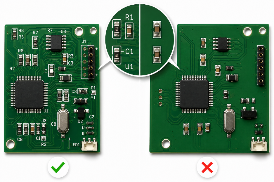
What Assembly Problems Can Missing Silkscreen Markings Cause?
Missing silkscreen markings can cause wrong placement, polarity errors, slower inspection, test confusion and higher rework cost. These problems can be reduced by keeping critical marks visible in Gerber files, assembly drawings and first article inspection.
- Wrong component placement
Missing reference designators make it harder to match the PCB with the BOM and pick-and-place file. This can slow down SMT setup and manual assembly.
Solution: keep key reference designators visible for ICs, connectors, polarized parts, jumpers and test-related components. - Reversed polarity parts
LEDs, diodes, electrolytic capacitors, optocouplers and ICs may be installed in the wrong direction if polarity marks or pin 1 indicators are missing. This can cause functional failure after power-on.
Solution: protect polarity marks first during layout and CAM review, especially near D1, LED1, C polarity marks and U1 pin 1. - Connector assembly mistakes
Missing connector labels can cause cable direction errors, wrong port connection or incorrect harness assembly. This is common in control boards, power modules and box-build PCBA projects.
Solution: label power input, signal output, communication ports and connector orientation clearly on the silkscreen or assembly drawing. - Slower manual inspection
Inspectors need more time to compare the physical PCB with drawings when component markings are absent. This increases inspection workload and may delay batch release.
Solution: confirm that top and bottom silkscreen markings are readable in the final Gerber viewer before production. - Test point confusion
Missing TP, GND, VCC, UART, SWD or programming labels can lead to wrong probing during ICT, FCT or debugging. Incorrect test contact may damage the board or produce false failure results.
Solution: mark key test points clearly and keep test labels outside component shadow areas after assembly. - Higher rework risk
Repair teams may remove or replace the wrong component when reference labels are missing. This increases rework time and may damage pads, traces or nearby components.
Solution: keep service-related labels visible and provide a matching repair drawing for dense PCBA boards. - Traceability gaps
Missing revision codes, date marks, customer part numbers or batch labels can cause confusion during incoming inspection, warranty analysis or repeat orders.
Solution: define required revision, batch and customer identification marks in the purchase file before fabrication.
How Does AOI Detect Missing Silkscreen Text and Markings?
AOI detects missing silkscreen text and markings by comparing board images with approved Gerber data, inspection programs or golden samples. It can identify missing text, broken characters, shifted labels and poor contrast.
Automated optical inspection uses controlled lighting and cameras to capture the PCB surface. The system then checks whether expected shapes, text blocks and symbols appear in the correct position. For small markings, image resolution and solder mask contrast are important because weak contrast may look like missing text.
PCB quality inspection missing text markings should also include manual review for critical areas. AOI is useful for repeatable checks, but human confirmation is still valuable for board revision codes, customer logos, warning labels and special compliance marks.
Quality control should check:
- Presence: required marks appear on the correct side.
- Position: text is not shifted into pads or components.
- Legibility: markings are readable after printing and curing.
- Contrast: ink color is clear against solder mask color.
- Completeness: characters are not broken, clipped or blocked.
- Traceability: revision, batch and customer marks are correct.
For bare PCB inspection, visual acceptability is often controlled by IPC-A-600 requirements. For assembled boards, visual workmanship is commonly checked with IPC-A-610 requirements. Customer drawings and approved samples should define the final acceptance rule.
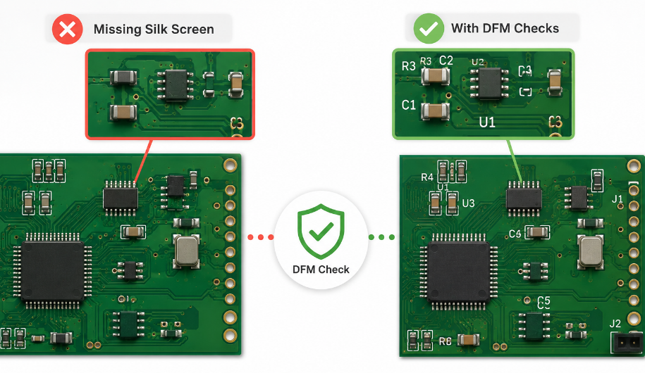
How to Prevent PCB Missing Silk Screen With DFM Checks?
PCB missing silk screen can be prevented when DFM checks review layer completeness, text clearance, readability and production risk before fabrication. The goal is to catch missing markings before the PCB enters manufacturing.
- Check silkscreen layer completeness
Confirm that top and bottom legend layers are included in the Gerber package. Missing overlay files are one of the most direct causes of blank or incomplete silkscreen. - Verify reference designators in Gerber view
Reference designators should be checked in the final Gerber files, not only in CAD software. This prevents hidden fields or non-print layers from reaching production. - Keep markings away from solderable areas
Silkscreen should not overlap pads, exposed copper or solder mask openings. Factories often remove overlapping ink to protect solder wetting and assembly reliability. - Prioritize critical orientation marks
Pin 1 marks, diode polarity, LED direction, capacitor polarity and connector labels should be protected first. These markings directly affect assembly accuracy. - Use readable text size and stroke width
Very small or thin text can become broken, faint or unreadable after printing. Readable markings reduce inspection errors and repair time. - Check both PCB sides separately
Top and bottom silkscreen should be reviewed side by side. Bottom-side labels are easy to miss during export, especially on double-sided SMT boards. - Review CAM clipping before production
If the factory must remove text near pads or board edges, the customer should approve the change before fabrication. This avoids unexpected missing markings after delivery. - Match silkscreen with BOM and assembly drawings
Component labels, polarity marks and connector names should match the BOM and assembly files. Mismatched documents can cause assembly confusion even when the silkscreen prints correctly. - Approve a first article sample
For batch production, the first article should confirm legibility, position, contrast and required marks. This prevents repeated PCB missing silk screen defects in mass production. - Define inspection requirements in the purchase file
Buyers should state required silkscreen color, revision mark, customer logo, UL mark, date code and acceptance criteria. Clear requirements reduce supplier misunderstanding and incoming QC disputes.
PCB Missing Silk Screen Project Case: From Gerber Error to Corrected Batch Production
A customer sent a four-layer industrial controller PCB for prototype and small batch production, but the original Gerber package had an empty top silkscreen layer. The PCB editor still showed reference designators, so the design team did not notice the export problem.
During incoming file review, the copper layers, solder mask, drill data and board outline were complete. However, the top overlay file had no useful text. Several LED polarity marks, connector labels and IC orientation marks were only visible in the assembly drawing, not in the Gerber data.
EBest Circuit reported the PCB missing silk screen risk before manufacturing. The customer regenerated the Gerber files with the correct top overlay settings. Our CAM team then checked pad clearance, removed only non-critical overlapping text and protected the polarity and connector markings.
After the corrected first article sample was approved, the batch moved into production. The final boards had readable reference designators, clear polarity marks and correct revision labels. Assembly questions decreased, and the customer avoided a batch of boards that would have been electrically correct but difficult to assemble.
FAQs About PCB Missing Silk Screen
Q1: Does missing silkscreen mean the PCB must be scrapped?
A1: Not always. If the copper circuit, solder mask, drill holes and solderability are correct, the PCB may still be usable. However, if missing markings affect polarity, testing, traceability or customer inspection, the batch may need rework, remarking or rejection. For production orders, the decision should follow the approved drawing and quality agreement.
Q2: Which components are most risky when silkscreen markings are missing?
A2: The highest-risk parts are direction-sensitive components, including LEDs, diodes, electrolytic capacitors, ICs, optocouplers and connectors. If polarity or pin 1 marks are missing, one wrong placement can cause functional failure. These markings should be treated as critical assembly information, not decorative text.
Q3: Can missing silkscreen be repaired after PCB fabrication?
A3: It can sometimes be repaired with manual labels, ink marking or controlled reprinting, but this is not ideal for batch production. Manual repair may look inconsistent and may not meet customer inspection requirements. The better solution is to correct the Gerber or CAD file and confirm the next batch before production.
Q4: What should buyers check before approving PCB production files?
A4: Buyers should open the final Gerber files and check top silkscreen, bottom silkscreen, reference labels, polarity marks, connector names, revision codes and customer logos. The BOM and assembly drawing should also match the board markings. This review can prevent avoidable batch defects before the order enters fabrication.
Q5: Does silkscreen affect solderability?
A5: Correctly placed silkscreen should not affect solderability. Problems happen when ink overlaps solder pads, exposed copper or solder mask openings. In that case, the factory may remove or clip the marking during CAM review. This is why clearance around pads is important for both clean printing and reliable solder joints.
Q6: Why do some PCB factories remove part of the silkscreen automatically?
A6: Factories often remove silkscreen that crosses pads, vias, exposed copper or board edges. The purpose is to avoid ink contamination, soldering defects and unreadable markings. If the removed text is important, the layout should be adjusted before fabrication so critical labels remain clear and printable.
Q7: Is white silkscreen always the best option?
A7: White silkscreen is common because it has good contrast on green solder mask, but it is not always the best choice. Black, yellow or gray ink may be better for special solder mask colors. The key requirement is clear contrast, stable adhesion and readability after soldering.
Q8: Should every component have a reference designator printed on the PCB?
A8: Not every component must be marked if the board is very dense, but critical parts should be identifiable. Priority should go to polarized components, ICs, connectors, test points, jumpers and service-related parts. For small passive components, the assembly drawing can support placement when space is limited.
Q9: How can silkscreen problems affect PCB assembly cost?
A9: Missing or unclear markings can increase manual checking, slow down inspection and raise rework risk. The cost impact may be small for one prototype, but significant in batch production. If operators must repeatedly compare the PCB with drawings, assembly time and quality control workload both increase.
Q10: Can silkscreen be hidden after components are assembled?
A10: Yes. Large components, connectors, shields, heat sinks or modules can cover silkscreen after assembly. Important markings should be placed where they remain visible during testing, repair and final inspection. If space is limited, critical labels can be moved near the component instead of directly under it.
Q11: What is the difference between silkscreen and assembly drawing information?
A11: Silkscreen provides quick visual guidance directly on the PCB, while the assembly drawing provides complete placement, orientation and process instructions. They should support each other. For dense PCB assembly, silkscreen improves speed, but the assembly drawing remains the full production reference document.
Q12: How should a supplier report silkscreen changes during CAM review?
A12: The supplier should clearly report any removed, clipped, shifted or simplified markings before fabrication. The report should include the affected area, reason for adjustment and updated preview. This allows the customer to approve the change or revise the layout before production begins.
Q13: Can PCB missing silk screen affect product traceability?
A13: Yes. If board revision, date code, batch number, customer part number or compliance mark is missing, traceability becomes weaker. This can create problems during incoming inspection, field repair or warranty analysis. For industrial and regulated products, traceability marks should be checked before production release.
Q14: What should be included in a silkscreen requirement for suppliers?
A14: A clear requirement should include silkscreen color, required side, minimum text size, revision mark, logo, polarity marks, connector labels and acceptance criteria. For batch orders, buyers should also request a first article photo. This helps avoid misunderstanding between design, purchasing and manufacturing teams.
Q15: When should a PCB batch be held because of silkscreen issues?
A15: A batch should be held when missing markings affect polarity, safety, testing, traceability or customer-approved artwork. Minor cosmetic differences may be acceptable only if they do not affect use or inspection. The final decision should follow the drawing, purchase order and agreed quality standard.
Conclusion
PCB missing silk screen is usually not an electrical circuit failure, but it can become a serious production risk when reference designators, polarity marks, connector labels, test points or revision codes are missing. The best solution is to catch the problem before fabrication by checking Gerber layers, CAD visibility, text clearance, CAM changes and first article samples.
For design teams, keep critical markings readable and protect orientation labels before export. For buyers, choose a PCB manufacturer that performs DFM review, checks missing legend layers, reports CAM adjustments and confirms marking quality before shipment. If you need custom PCB fabrication, PCBA assembly or batch production support, send your Gerber files, BOM and assembly requirements to EBest Circuit via sales@bestpcbs.com for a fast quotation.