





Network monitoring PCB manufacturing requires accurate impedance control, reliable assembly, and stable operation under continuous network traffic. Incorrect trace geometry, connector misalignment, or soldering defects may cause communication errors, unstable links, and repeated prototype failures. How can you identify these manufacturing risks before they affect your project schedule?
EBest Circuit provides network monitoring PCB fabrication, prototyping, component sourcing, and SMT/THT assembly. With 20 years of PCB manufacturing experience, standard FR4 manufacturing from 1–10 layers, and special processes supporting up to 32 layers, we help customers meet demanding manufacturing requirements. Our free DFM check identifies potential manufacturability concerns before fabrication.
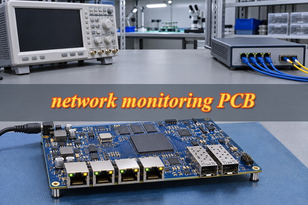
What Are Network Monitoring PCBs Used For?
Network monitoring PCBs are used in equipment that captures, measures, analyzes, and records network activity, including traffic volume, packet transmission, link status, communication errors, and network performance.
Unlike ordinary network device PCBs, network monitoring boards may need to support continuous data acquisition, accurate event timing, and reliable operation under sustained traffic loads.
Common applications include:
- Network traffic monitoring equipment: Captures network traffic for bandwidth analysis, performance monitoring, and fault investigation.
- Packet capture and protocol analyzers: Connects Ethernet interfaces, processors, and memory circuits for packet inspection and recording.
- Network TAP equipment: Provides connections and monitoring paths for observing network traffic.
- Optical network monitoring devices: Integrates SFP/SFP+ interfaces, management circuits, and processing modules for optical link monitoring.
- Industrial network diagnostic systems: Monitors Ethernet connectivity, communication errors, and equipment status in industrial networks.
A monitoring board using a 100 Mb/s Ethernet interface does not have the same routing and signal-integrity requirements as a multiport 10 Gb/s packet analyzer.
The PCB stackup, materials, routing density, and inspection requirements should match the actual interface speed and equipment configuration.
What Are the Key Design Requirements for Network Monitoring PCBs?
Network monitoring PCB design must establish measurable impedance, signal timing, power, thermal, and mechanical requirements before fabrication. The selected Ethernet PHY, MAC, or transceiver specification determines the applicable electrical limits.
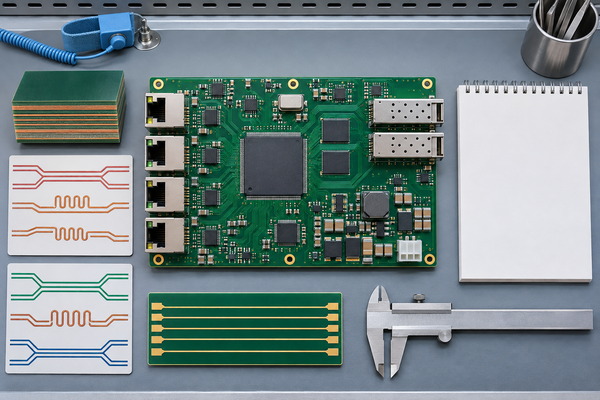
The following values are engineering references for specific Ethernet PHY interfaces, not universal rules for every network monitoring PCB.
| Design Parameter | Engineering Reference | Application and Verification |
|---|---|---|
| Ethernet MDI Differential Impedance | 100 Ω | Common PHY-to-magnetics interface requirement |
| Ethernet MDI Single-Ended Impedance | 50 Ω | Referenced to the specified ground plane |
| SGMII Differential Impedance | 100 Ω | Applicable SGMII PHY interfaces |
| SGMII Intra-Pair Skew | Less than 5 ps | Example requirement for compatible PHY devices |
| RGMII Single-Ended Impedance | 50 Ω | Applicable PHY-to-MAC interface |
| RGMII TX Data-Group Skew | Less than 11 ps | Example PHY-specific data-lane matching requirement |
| RGMII RX Data-Group Skew | Less than 11 ps | Example PHY-specific data-lane matching requirement |
| RGMII Trace Length | Below 50.8 mm preferred | Example PHY recommendation; device-specific limits apply |
Ethernet MDI, SGMII, and RGMII require different routing rules. The impedance and timing limits for one interface should not be automatically applied to another. High-speed SFP+ links must follow their specific transceiver and channel requirements.
PCB stackup construction directly affects whether the routing targets can be achieved. Trace width, spacing, copper thickness, dielectric thickness, and reference-plane position must be evaluated together.
For example, a 100 Ω differential pair does not have a fixed trace width across different FR4 stackups. Changing copper thickness or dielectric configuration may require different conductor dimensions.
Other important design considerations include:
- Power integrity: Verify supply voltage tolerances, decoupling placement, and current requirements against the selected IC specifications.
- Clock stability: Confirm oscillator accuracy, reference-clock routing, and timing requirements for the selected monitoring architecture.
- EMI/ESD protection: Design shielding, grounding, return paths, and interface protection according to the equipment’s applicable requirements.
- Thermal management: Keep processor and interface-component temperatures within their specified operating limits.
- Mechanical integration: Confirm board thickness, mounting-hole positions, connector dimensions, and enclosure clearances.
For monitoring equipment that records precise event timestamps, clock accuracy and timing behavior require appropriate system-level validation.
Controlled-impedance PCB manufacturing supports signal integrity, but it does not independently guarantee packet-capture accuracy or timestamp precision.
What Are the Common Network Monitoring PCB Design and Manufacturing Challenges and Solutions?
Network monitoring equipment manufacturers frequently encounter unstable high-speed links, limited routing space, connector assembly problems, and inconsistent production results. EBest Circuit addresses manufacturing-related risks through engineering review, appropriate fabrication processes, and assembly inspection.
Challenge: Network links become unstable after prototype assembly.
Unexpected link drops, excessive communication errors, or failure to establish the required connection speed may result from impedance discontinuities, connector defects, soldering problems, or circuit-level faults.
Our solution: We review the approved stackup, critical trace geometry, via structures, and connector requirements before fabrication. Controlled-impedance measurements and relevant inspections can be arranged according to the project specification. Assembly-related defects are addressed through the agreed inspection process, while complete link performance is verified through customer-defined functional testing.
Challenge: High-density components exceed conventional routing limits.
FPGAs, network processors, memory devices, and fine-pitch ICs may require dense routing around component pads. Insufficient spacing or inappropriate drilling structures can prevent successful PCB fabrication.
Our solution: EBest Circuit evaluates the proposed routing density, copper weight, drill structure, and layer count. Our special FR4 processes support 3/3 mil line/space and 0.10 mm laser microvias under applicable manufacturing conditions. We also assess whether conventional multilayer construction can meet the design requirements without unnecessary HDI processing.
Challenge: Network connectors do not align with the equipment enclosure.
RJ45 connectors, SFP/SFP+ cages, and board-edge interfaces require accurate mechanical positioning. Incorrect board dimensions or connector placement may cause assembly problems or mechanical stress.
Our solution: We check board outlines, mounting-hole dimensions, connector footprints, and relevant tolerances against the supplied manufacturing drawings. Connector positioning and soldering quality can be included in the assembly inspection plan.
Challenge: Prototype performance changes during repeat production.
Material substitutions, PCB revisions, component changes, and soldering-process variations may affect production consistency.
Our solution: We coordinate production using the customer’s approved PCB files, BOM revisions, assembly requirements, and inspection criteria. Proposed changes are reviewed before implementation, helping maintain a consistent manufacturing configuration.
How Are Network Monitoring PCB Prototypes Fabricated and Assembled?
Network monitoring PCB prototyping follows a sequence of engineering review, bare-board fabrication, component assembly, inspection, and functional verification. Each stage helps identify potential problems before the design enters volume production.
Step 1 — Review PCB and Assembly Files
The manufacturing review covers Gerber or ODB++ files, drill data, PCB stackup, BOM, pick-and-place files, and assembly drawings.
Our free DFM check examines trace spacing, drilling feasibility, stackup requirements, solder mask openings, and relevant assembly clearances.
Manufacturing questions are confirmed with the customer before production release.
Step 2 — Fabricate the Bare PCB
PCB fabrication follows the approved material, copper weight, layer structure, drilling requirements, and surface finish.
Depending on the construction, manufacturing includes inner-layer imaging and etching, lamination, drilling, metallization, outer-layer processing, solder mask application, and surface finishing.
For controlled-impedance designs, the required conductor geometry and stackup are confirmed before fabrication.
Step 3 — Inspect the Fabricated PCB
Electrical testing checks continuity and isolation against the approved netlist.
AOI, dimensional inspection, and additional specified measurements help identify manufacturing defects before component assembly.
Step 4 — Verify Components and Prepare Assembly
The approved BOM is checked for manufacturer part numbers, package compatibility, quantities, and component availability.
Stencil preparation and placement-program verification are completed before SMT production. Any proposed component substitution requires customer approval.
Step 5 — Perform SMT Assembly
Solder paste is applied to the appropriate pads, followed by component placement and controlled reflow soldering.
SPI and AOI are used according to the assembly inspection requirements. X-ray inspection can be arranged for suitable packages with hidden solder joints.
Step 6 — Complete THT Assembly
RJ45 connectors, headers, and other through-hole components are installed using the appropriate soldering process.
Connector alignment, mechanical positioning, and solder-joint quality are checked according to the assembly requirements.
Step 7 — Program and Functionally Test the PCBA
When the required firmware, fixtures, and test procedures are available, functional verification may include:
- Ethernet link establishment at the specified interface speed.
- Port communication and packet-transfer testing.
- Power-rail voltage and current measurements.
- Clock or timestamp verification against a defined reference.
- Sustained operation under specified traffic loads.
Step 8 — Perform Final Inspection and Shipment Preparation
The approved PCB revision, BOM, assembly condition, identification requirements, and agreed inspection records are checked before packaging.
Prototype approval should be based on the customer’s measurable electrical, mechanical, and functional acceptance criteria. A successfully assembled PCB is not automatically a fully qualified network monitoring system.
What Network Monitoring PCB Manufacturing and Assembly Services Does EBest Circuit Provide?
EBest Circuit supports network monitoring PCB projects from design-for-manufacturing review to finished PCBA delivery. Our manufacturing services can be selected according to the customer’s approved design, component requirements, and production plan.
- PCB Design for Manufacturability Support: Review stackup feasibility, controlled impedance, fine-line routing, drilling, solder mask, and assembly requirements.
- Custom PCB Fabrication: Manufacture FR4 multilayer boards and suitable HDI constructions according to approved production files.
- PCB Prototyping: Support engineering samples and pilot builds before volume production.
- Component Sourcing: Procure approved Ethernet PHYs, processors, memory devices, passive components, and network interface connectors.
- SMT and THT Assembly: Assemble surface-mount and through-hole components, including mixed-technology PCBA.
- Programming and Testing Support: Arrange applicable inspection, firmware programming, and customer-defined functional testing when the required resources are available.
For customers requiring both PCB fabrication and assembly, these services can be coordinated through a single manufacturing project.
The standard free DFM check focuses on the manufacturability of customer-provided designs. Original circuit development or complete PCB layout design requires separate project confirmation.
What Are Our Network Monitoring PCB Manufacturing and Assembly Capabilities?
EBest Circuit supports FR4 PCB manufacturing from standard multilayer boards to high-density special-process constructions. Our capabilities help engineers evaluate the feasibility of network monitoring PCBs with dense interfaces, fine-pitch packages, and multilayer routing.
| Manufacturing Capability | Standard Process | Special Process |
|---|---|---|
| FR4 Layer Count | 1–10 layers | 10–32 layers |
| Inner-Layer Line/Space, 0.5–1 oz Copper | 4/4 mil | 3/3 mil |
| Outer-Layer Line/Space, 1 oz Copper | 4/4 mil | 3/3 mil |
| Outer-Layer Line/Space, 2 oz Copper | 8/8 mil | 6/6 mil |
| Laser Microvia Diameter | 0.10 mm | 0.10 mm, subject to construction review |
| Minimum Finished Mechanical Hole | 0.20 mm | 0.15 mm |
| Maximum Through-Hole Aspect Ratio | 8:1 | 10:1 |
| PTH Hole Diameter Tolerance | ±3 mil | ±2 mil |
| NPTH Hole Diameter Tolerance | ±2 mil | ±1 mil |
Manufacturing limits must be evaluated as a complete PCB construction. Minimum line spacing, minimum finished hole size, maximum layer count, and maximum aspect ratio are not automatically achievable together.
Actual feasibility depends on copper thickness, finished board thickness, laminate properties, layer stackup, plating requirements, drilling structures, and other process conditions.
For high-density network monitoring PCBs, the approved design should be evaluated against these combined requirements before fabrication.
Assembly feasibility is assessed separately according to component packages, connector geometry, soldering requirements, and inspection access.
How Do We Ensure Network Monitoring PCB Quality and Reliability?
Network monitoring PCB quality is verified through bare-board inspection, PCBA workmanship checks, and customer-defined functional testing. These methods address different manufacturing and operational risks.

Bare-Board Quality Control
- AOI: Identifies visible conductor-pattern defects.
- Electrical Testing: Checks continuity and isolation against the approved PCB netlist.
- Impedance Measurement: Verifies specified controlled-impedance structures when required.
- Dimensional Inspection: Checks board outlines, mounting holes, and other critical dimensions.
PCBA Quality Control
- SPI: Evaluates solder-paste deposits before component placement.
- AOI: Identifies visible placement and soldering defects.
- X-ray Inspection: Examines hidden joints where required.
- Connector Inspection: Checks mechanical alignment and soldering condition.
Network Monitoring Functional Verification
A monitoring device may require testing at its intended link speed, port configuration, and operating load.
For example, a multiport monitoring PCBA can be evaluated for link establishment, communication errors, supply stability, and sustained operation under the specified traffic conditions.
When event timestamping is required, the test plan should identify the reference source, measurement method, and acceptable timing error.
Bare-board electrical testing cannot independently verify packet-capture accuracy, timing precision, or complete network monitoring performance. These characteristics require appropriate assembled-system validation.
What Quality Certifications Support Our Network Monitoring PCB Production?
EBest Circuit maintains quality management certifications that support production control, manufacturing traceability requirements, and supplier qualification.
Our quality certification portfolio includes:
- ISO 9001:2015: General quality management covering production processes, inspection, and corrective actions.
- ISO 13485:2016: Medical device quality management for applicable manufacturing activities.
- IATF 16949: Automotive quality management for applicable electronics manufacturing programs.
- AS9100D: Aerospace quality management for applicable high-reliability manufacturing requirements.
For commercial and industrial network monitoring PCB projects, ISO 9001 is the primary general quality-management reference. Industry-specific certifications may be relevant to medical, automotive, or aerospace applications.
Customers can request applicable certificate copies and verify the certificate holder, manufacturing site, scope, and validity before supplier approval.
Network Monitoring PCB Prototyping and Assembly Case Study
A compact Ethernet traffic monitoring module illustrates how PCB manufacturing and assembly requirements can be evaluated before prototype production.
The following is an engineering application example using representative design requirements.
Project Background
Consider a compact network monitoring module integrating Ethernet PHY circuitry, processing components, memory, and network connectors.
The proposed construction uses a 4-layer FR4 PCB with a finished thickness of 1.6 mm, 1 oz outer copper, and ENIG surface finishing.
Project Requirements and Challenges
The PCB requires controlled-impedance routing, suitable layer-stackup design, accurate connector positioning, and reliable SMT assembly.
The principal manufacturing concerns are maintaining the specified conductor geometry, confirming enclosure compatibility, and ensuring that the assembled PCB can be tested against the required communication functions.
Manufacturing Approach
The production review would confirm stackup, copper weight, trace spacing, drilled-hole requirements, solder mask openings, and connector dimensions.
For 1 oz outer copper, EBest Circuit supports 4/4 mil standard line/space and 3/3 mil special-process line/space, subject to the applicable manufacturing conditions.
After fabrication, bare-board electrical inspection and the agreed assembly inspection procedures would be performed.
Qualification Requirements
Prototype approval would require verification of PCB dimensions, electrical continuity, connector alignment, assembly quality, Ethernet link operation, and specified traffic or timing requirements.
The customer-defined test plan must establish the measurement methods and pass/fail limits before production release.
Why Choose EBest Circuit for Network Monitoring PCB Prototyping and Assembly?
With 20 years of PCB manufacturing experience, advanced FR4 fabrication, and integrated PCBA services, EBest Circuit supports network monitoring projects from prototype review to volume production.
- 20 Years of Manufacturing Experience: Since 2006, we have supported complex PCB projects, helping customers address stackup, drilling, and fabrication challenges before production.
- Advanced PCB Capabilities: We support up to 32 FR4 layers, 3/3 mil line/space, and 0.10 mm laser microvias under applicable conditions, meeting the needs of high-density monitoring equipment.
- One-Stop PCB & PCBA Services: PCB fabrication, component sourcing, SMT/THT assembly, and testing support are coordinated through one supplier, simplifying procurement and production.
- Certified Quality Management: Our certifications include ISO 9001, ISO 13485, IATF 16949, and AS9100D, supporting supplier qualification for applicable industrial and specialized applications.
- Free DFM & Flexible Production: We identify manufacturability issues before fabrication and support prototypes, small batches, and volume production, helping customers reduce revisions and prepare for repeat orders.
EBest Circuit combines manufacturing capability, quality management, and assembly services to support reliable network monitoring PCB production.
What Is the Lead Time for Network Monitoring PCB Prototyping and Mass Production?
Network monitoring PCB lead time depends on layer count, materials, drilling requirements, controlled impedance, component availability, and assembly complexity.
For qualifying standard FR4 PCB prototype orders below 1 m², our reference manufacturing lead times are:
- 2-layer PCB: Approximately 8 days.
- 4-layer PCB: Approximately 10 days.
- 6-layer PCB: Approximately 10 days.
- 8-layer PCB: Approximately 12 days.
- 10-layer and higher: Confirm according to the project specifications.
These standard reference schedules apply to qualifying FR4 designs with conditions such as 0.4–1.6 mm board thickness, 0.5 oz or 1 oz copper, lead-free HASL, line/space above 8 mil, and finished holes above 0.3 mm.
For projects meeting expedited-service requirements, faster prototype manufacturing may be available after engineering review and production scheduling.
Network monitoring PCBs requiring ENIG, fine-line routing, controlled-impedance inspection, HDI structures, or special materials may follow different manufacturing schedules.
PCBA assembly lead time must be calculated separately from bare-board fabrication. Component procurement, stencil preparation, programming, inspection, and functional testing must be included when establishing the complete production schedule.
International transportation and customs clearance are not included in manufacturing lead time unless specified in the quotation.
What Factors Affect Network Monitoring PCB Manufacturing and Assembly Costs?
Network monitoring PCB costs depend on PCB construction, materials, manufacturing processes, component procurement, assembly complexity, and testing requirements. The most effective cost reductions usually come from avoiding unnecessary manufacturing complexity while preserving the approved electrical and reliability requirements.
Practical cost-reduction methods include:
- Avoid unnecessary HDI structures: Use conventional multilayer through-hole routing where component escape and signal-integrity requirements permit. Reserve laser vias and sequential lamination for designs that actually need them.
- Use standard line/space where possible: If 4/4 mil routing satisfies the approved design, special 3/3 mil processing may not be necessary.
- Select copper weight according to actual requirements: Choose 1 oz, 2 oz, or heavier copper based on current and thermal requirements. Increasing copper thickness unnecessarily may create tighter manufacturing constraints.
- Choose a suitable surface finish: Select ENIG, OSP, or another approved finish based on assembly, storage, and application requirements rather than specifying a more expensive finish without a technical reason.
- Review the BOM before prototype release: Identify unavailable, obsolete, or long-lead components. Evaluate alternative parts early, with customer engineering approval.
- Improve panel utilization: Optimize the board outline and panel arrangement where manufacturing and mechanical constraints allow.
- Compare prototype and volume pricing: Request separate quotations for prototype, pilot, and production quantities using consistent design revisions.
- Define testing requirements early: Avoid unnecessary duplicate tests while retaining the inspections and functional checks needed for product acceptance.
Do not reduce PCB layer count or remove necessary reference planes solely to lower fabrication costs. For high-speed network monitoring equipment, these changes may increase signal-integrity problems and lead to additional redesign expenses.
A complete quotation should distinguish PCB fabrication, component purchasing, assembly, testing, tooling, and applicable one-time charges.
FAQs About Network Monitoring PCB Design, Prototyping and Assembly
Q1. Can an NDA be signed before sharing confidential network monitoring PCB files?
A1. Yes. A non-disclosure agreement can be discussed and signed before confidential Gerber files, BOMs, circuit drawings, or other proprietary technical information are exchanged. The confidentiality scope should be confirmed in advance.
Q2. What files are required for a network monitoring PCBA quotation?
A2. Provide Gerber or ODB++ files, drill data, fabrication drawings, BOM with manufacturer part numbers, pick-and-place files, assembly drawings, quantity, required delivery date, and delivery location. Include programming and functional test specifications where applicable.
Q3. Can customers supply their own network processors, PHYs, or connectors?
A3. Customer-supplied components can be evaluated for assembly. Part numbers, quantities, packaging, moisture sensitivity, and component condition should be confirmed before production.
Q4. What happens if an approved Ethernet PHY becomes unavailable?
A4. The component shortage should be identified during BOM review. Proposed alternatives require evaluation of pinout, electrical specifications, package compatibility, firmware dependencies, and qualification requirements. Substitutions must be approved before procurement or assembly.
Q5. Can different PCB revisions be manufactured under one project?
A5. Yes. Each PCB revision must be identified and controlled separately. The manufacturing files, BOM, assembly instructions, and inspection requirements must correspond to the correct approved revision.
Q6. Can customers provide firmware and functional test fixtures?
A6. Customer-provided firmware, programming instructions, and test fixtures can be evaluated. The required equipment, interfaces, and pass/fail criteria should be agreed before testing.
Q7. Can inspection records be provided with the PCBA shipment?
A7. Required inspection documentation can be discussed during quotation. Depending on the agreed scope, records may include bare-board electrical test results, impedance measurements, dimensional inspection, or assembly inspection reports.
Q8. Can PCB and component lot traceability be specified?
A8. Yes. Traceability requirements can be reviewed before production. Customers should specify the required PCB lot identification, component batch information, serial numbers, and related record requirements.
Q9. Can network monitoring PCBAs be supplied with special ESD protection?
A9. Packaging requirements can be specified according to ESD sensitivity, connector protection, mechanical handling, and transportation conditions. Special packaging arrangements should be confirmed during order preparation.
Q10. Can network monitoring PCBA orders be delivered in separate shipments?
A10. Split shipments can be discussed according to the production schedule. The quantity, inspection status, delivery destination, and shipping arrangements for each shipment must be agreed in advance.
Looking for a network monitoring PCB manufacturer that combines advanced PCB fabrication capabilities with assembly and production support? EBest Circuit provides custom FR4 PCB manufacturing, multilayer and HDI fabrication, SMT/THT assembly, component sourcing, and agreed testing services to support your project from prototypes to volume production.
Send your Gerber files, BOM, assembly drawings, quantity, required delivery date, and delivery location to sales@bestpcbs.com. Get a free DFM check and a project-specific quotation covering PCB manufacturing, assembly, testing requirements, and lead time.
You may also like




Tags: Network Monitoring PCB, Network Monitoring PCB Assembly, Network Monitoring PCB Design, Network Monitoring PCB Prototyping