PCB manufacturing PCB manufacturing
Home > Blog

Heavy Copper PCB Manufacturing

How to Compare Heavy Copper PCB Manufacturers in Canada?
Saturday, September 26th, 2026

Choosing among heavy copper PCB manufacturers in Canada requires more than comparing copper weight, certifications, or unit price. Two suppliers may both advertise 10 oz or 20 oz copper, yet differ significantly in the stackups they can build, the inspection records they provide, the actual production site, and the time required to deliver finished boards to Canada.

To compare heavy copper PCB manufacturers in Canada fairly, buyers should use the same PCB specification and review six areas together: manufacturing capability, production location, quality evidence, certifications, total quoted cost, and lead Time. The sections below show how to compare those factors, how domestic and overseas supply routes differ, and what information to include in an RFQ before choosing a supplier.
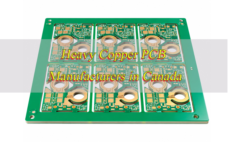
Heavy Copper PCB Manufacturers in Canada, https://www.bestpcbs.com/blog/2026/09/heavy-copper-pcb-manufacturers-in-canada/

What Should You Compare When Evaluating Heavy Copper PCB Manufacturers in Canada?

A useful comparison starts with the actual PCB, not with a manufacturer’s general capability page. The supplier must be able to manufacture the required construction and support it with clear quality and commercial terms.

  • Manufacturing capability: Confirm finished copper, trace width and spacing, layer count, board thickness, plated holes, and laminate in the same stackup.
  • Quality evidence: Check what records are available for copper thickness, plated-hole quality, electrical testing, dimensions, and first-article inspection.
  • Certifications: Verify that the required quality system covers the manufacturing site used for the order.
  • Pricing: Compare material, tooling, testing, documentation, freight, and import-related costs on the same basis.
  • Lead Time: Determine whether the quoted schedule covers fabrication only or delivery to the final Canadian destination.
  • Manufacturing location: Identify whether the board will be fabricated in Canada, through an offshore partner, or directly by an overseas factory.

The lowest price or highest advertised copper weight does not automatically indicate the better supplier. A quote is only meaningful when it reflects the same board construction, inspection scope, quantity, and delivery basis.

Which Heavy Copper PCB Manufacturers in Canada Serve Canadian Projects?

Canadian buyers can source heavy copper PCBs from domestic factories, Canadian companies coordinating offshore production, or overseas manufacturers shipping directly to Canada. These routes can all serve Canadian projects, but the actual production site should be clear before quotations are compared.

ManufacturerManufacturing RoutePublished Heavy Copper CapabilityTypical Fit
CCI Canadian CircuitsCanadaPublished range from 1 oz to 40+ ozProjects requiring Canadian fabrication
Candor IndustriesCanadaHeavy copper from 3 ozDomestic prototypes and custom PCB programs
J-Cube TechnologiesCanadian coordination with offshore partnersPublished 2 oz to 20 ozBuyers wanting Canadian commercial support with offshore production
Bittele ElectronicsInternational manufacturing networkPublished multilayer capability up to 10 ozPCB and PCBA programs using an international production route
EBest CircuitShenzhen, ChinaHeavy copper PCB manufacturing for international projectsCanadian projects that permit direct overseas fabrication

The office location of a supplier does not always show where the PCB is produced. Before comparing heavy copper PCB manufacturers in Canada, confirm the actual factory, certification coverage, and manufacturing origin used for the quoted order.

Canadian vs. Overseas Heavy Copper PCB Manufacturers: What’s the Difference?

The choice between Canadian and overseas manufacturing depends on origin requirements, technical capability, total delivered cost, and the amount of international logistics the project can accept. Neither route is automatically better.

Factor Buyers Care AboutCanadian ManufacturingOverseas Manufacturing
Manufacturing originPCB is fabricated in CanadaPCB is fabricated outside Canada
Supplier optionsLimited to available domestic capabilityBroader range of factories, stackups, and production capacities
Cost structureFactory and domestic commercial costsFactory cost plus freight, customs, and import-related charges
Lead TimeShorter logistics route, but material and factory loading still matterFabrication plus international freight, customs, and delivery in Canada
Engineering communicationEasier time-zone alignmentTime-zone differences may affect communication
Factory accessEasier for local audits or visitsMore planning may be required
CustomsNo international import process for domestic fabricationImport clearance and responsibility must be defined
Origin restrictionsSuitable when Canadian origin is requiredSuitable only when overseas manufacturing is permitted
Production capacityDepends on domestic factory capacityBroader supplier base may offer more volume options

If Canadian origin is mandatory, the supplier list becomes much narrower. If origin is unrestricted, compare both routes on technical capability, quality evidence, total delivered cost, and Lead Time rather than location alone.

Can the Manufacturer Build Your Heavy Copper PCB Stackup?

Maximum copper weight is only one part of manufacturability. A simple two-layer 10 oz PCB with wide conductors is much easier to build than a multilayer 10 oz board with small plated holes, tight spacing, and different copper weights across the stackup.

Before approving a supplier, confirm the complete construction:

  • Finished copper by layer: Do not rely on a general note such as “6 oz PCB.” State the finished copper requirement for every controlled layer.
  • Trace width and spacing: Confirm the geometry at the required copper thickness rather than using a generic minimum capability from the factory website.
  • Layer count and board thickness: Thick copper affects resin fill, copper balance, lamination, registration, and finished thickness.
  • Finished hole size and aspect ratio: Small plated holes through a thick board can become a constraint even when the copper weight is within the advertised range.
  • Barrel copper and annular ring: Review these together with board thickness and finished hole size.
  • Laminate: Confirm that the material suits the product’s electrical, thermal, assembly, and operating requirements.

This is why comparing heavy copper PCB manufacturers in Canada should start with the actual stackup. A factory may meet each specification individually but still be unable to manufacture that combination reliably.

How Can You Verify Heavy Copper PCB Manufacturing Quality?

Not all heavy copper PCB manufacturers in Canada provide the same level of inspection evidence. Buyers should verify what will be inspected, what reports will be available, and how those records link to the PCB revision and production lot.

  • Copper thickness measurement: Verify finished copper against the fabrication drawing, not only the incoming copper foil. If thickness is controlled, define whether the requirement is nominal, minimum, or subject to a stated tolerance.
  • AOI and conductor inspection: AOI can detect opens, shorts, residual copper, neck-down, and other conductor defects. These risks become more important as copper thickness increases and the etching process window narrows.
  • Microsection inspection: A representative cross-section can show plated-hole barrel copper, internal-layer connections, annular-ring condition, visible voids, and lamination quality.
  • Electrical testing: Continuity and isolation testing verifies the electrical network against the supplied netlist or design data. It does not replace physical inspection of copper thickness or plated holes.
  • Dimensional inspection: Finished board thickness, hole diameter, outline, and controlled mechanical dimensions should be checked against the released drawing.
  • First-article records: For a new supplier or stackup, first-article inspection can tie the approved material, construction, copper requirements, dimensions, test results, and accepted deviations to one revision.
  • Traceability: Production and lot records should make it possible to identify the required material and manufacturing history when the project calls for it.

A certificate or equipment list does not prove that an individual shipment meets specification. Order-level inspection records provide much stronger evidence of the finished PCB quality.
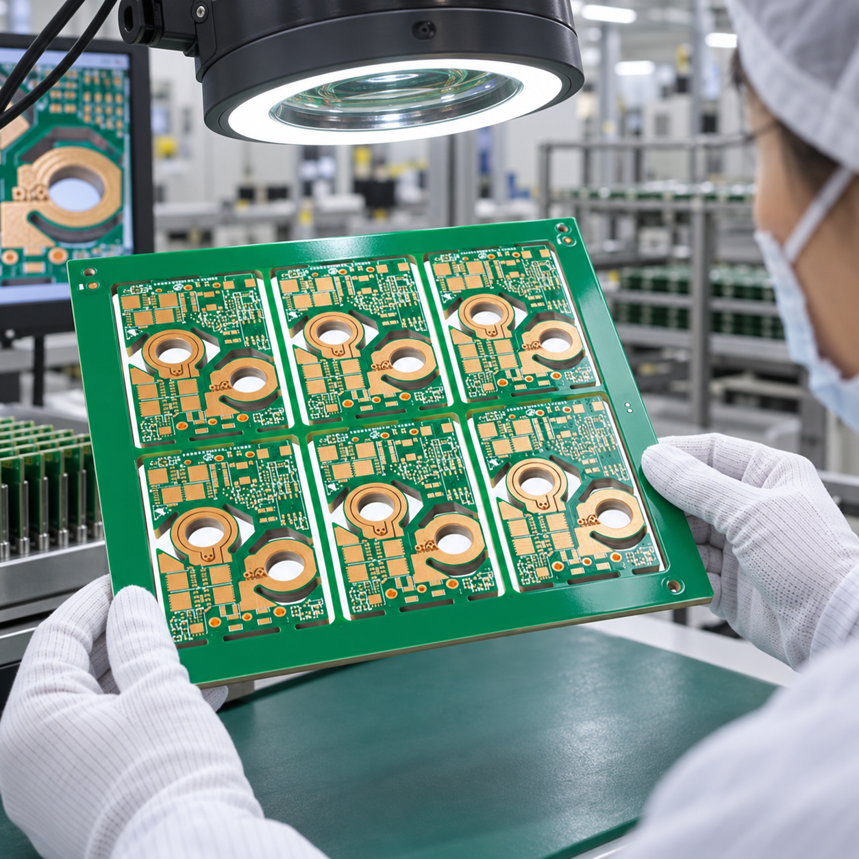
Heavy Copper PCB Manufacturers in Canada

Which Certifications Should Heavy Copper PCB Manufacturers in Canada Have?

The required certifications depend on the end market and customer requirements. More certificates do not automatically make a supplier more suitable; the relevant issue is whether the required system covers the site that will actually produce the PCB.

  • ISO 9001: Common quality-management foundation for industrial and commercial PCB programs.
  • IATF 16949: Relevant to automotive supply chains that require automotive quality-management controls.
  • ISO 13485: Relevant to medical-device programs where a medical quality-management system is required.
  • AS9100D: Relevant to aerospace and defense programs with aerospace quality requirements.
  • UL, RoHS, and REACH: May be required for product recognition, restricted substances, or material compliance, but they do not replace manufacturing quality-system certification.

When reviewing certificates from heavy copper PCB manufacturers in Canada, check the legal entity, manufacturing site, certification scope, and validity date rather than the certificate name alone.

How Should You Compare Quotes from Heavy Copper PCB Manufacturers in Canada?

One of the biggest differences between heavy copper PCB manufacturers in Canada is what each supplier includes in the quotation. A lower unit price may simply reflect a different stackup, reduced inspection scope, or different delivery terms.

  • Compare the same finished copper requirement. One supplier may interpret “6 oz” differently from another, particularly when outer-layer plating is involved.
  • Keep the stackup consistent. Layer count, dielectric thickness, finished board thickness, and approved materials should match.
  • Check geometry assumptions. Trace width, spacing, annular rings, and finished holes should not be changed without approval.
  • Compare the same laminate and surface finish. Material substitutions can change both cost and performance.
  • Match the inspection scope. Electrical testing, microsections, copper measurements, dimensional reports, and first-article records may not be included in every quote.
  • Separate tooling and NRE. Tooling, engineering, test fixtures, and special inspection charges should be clearly identified.
  • Use the same quantity. Prototype and production pricing follow very different cost structures.
  • Compare total delivered cost. Include packaging, freight, customs, import charges, and delivery terms where applicable.
  • Confirm the manufacturing site. If a specific site is approved in the quotation, it should not be changed without disclosure.

The useful question is not simply “Which supplier has the lowest unit price?” It is whether each supplier is quoting the same PCB construction, quality scope, quantity, and delivery basis.

How Should You Compare Lead Time from Heavy Copper PCB Manufacturers in Canada?

Lead time should be measured from the same starting point to the same delivery point. A quoted “10-day Lead time” has little meaning unless you know exactly what those 10 days include.

  • Engineering review: Confirm whether lead time starts when the RFQ is received, when engineering questions are resolved, or when production files are approved.
  • Material availability: Special laminates, unusual copper weights, or non-standard thicknesses may add sourcing time before fabrication starts.
  • Fabrication complexity: Layer count, thick-copper etching, plating, drilling, lamination, and inspection can all affect production time.
  • First-article approval: If production waits for customer approval, include that approval period in the schedule.
  • Inspection and documentation: Microsections, additional measurements, inspection reports, and traceability requirements may add time after fabrication.
  • International logistics: Overseas orders may require packaging, international freight, customs clearance, import handling, and domestic delivery within Canada.
  • Expedited production: Confirm whether the actual stackup and quantity qualify for fast-turn service rather than relying on the shortest advertised schedule.

Always distinguish factory lead time from delivered lead time. When comparing heavy copper PCB manufacturers in Canada, use the same approved-file date, quantity, shipping method, and Canadian destination.

What Should You Send to Heavy Copper PCB Manufacturers in Canada in an RFQ?

Sending the same RFQ package to heavy copper PCB manufacturers in Canada is the most practical way to obtain quotations that can be compared fairly. Missing information forces suppliers to make their own assumptions, which can distort both price and Lead Time.

  • Design files: Gerber or ODB++, NC drill files, fabrication drawing, netlist where applicable, and revision number.
  • Stackup: Layer count, laminate, dielectric requirements, finished board thickness, and finished copper by layer.
  • Critical geometry: Minimum trace width, spacing, finished hole sizes, annular-ring requirements, outline tolerances, and controlled mechanical features.
  • Surface finish: ENIG, HASL, OSP, or another finish, together with solder mask, legend, contacts, and edge requirements.
  • Quality requirements: Electrical testing, copper measurement, AOI, microsection, dimensional reports, first-article inspection, traceability, and the required acceptance standard.
  • Certifications: State any quality-system or customer-specific certification that must cover the production site.
  • Quantity: Include prototype quantity and expected production volume when available.
  • Delivery requirements: Provide the Canadian destination, required delivery date, preferred shipping method, and any manufacturing-origin restriction.
  • Commercial requirements: Ask the supplier to separate unit price, tooling/NRE, inspection charges, freight, and other non-recurring costs.

A complete RFQ should leave little room for interpretation. Finished copper by layer, controlled geometry, inspection scope, quantity, and delivery destination are especially important when comparing price and lead time.

Why Choose EBest Circuit for Heavy Copper PCB Manufacturing?

EBest Circuit is a China-based PCB manufacturer serving international projects. Its services include PCB design, PCB prototyping, mass production, component sourcing, and PCB assembly, allowing customers to manage more stages of a project through one supplier.

  • Move from prototype to volume production with fewer supplier changes. EBest Circuit supports both PCB prototyping and mass production, so buyers can develop, validate, and scale a project without rebuilding the supply chain at each stage.
  • Combine PCB fabrication, sourcing, and assembly with one supplier. Component sourcing and PCB assembly can be added when required, reducing the time spent coordinating separate PCB, component, and assembly vendors.
  • Support projects with demanding quality-system requirements. EBest Circuit lists IATF 16949, ISO 9001:2015, ISO 13485:2016, and AS9100D, providing relevant quality-system support for automotive, industrial, medical, and aerospace programs.
  • Source different PCB technologies through the same manufacturing partner. Alongside heavy copper PCBs, EBest Circuit supports multilayer, metal-core, ceramic, rigid-flex, RF, High Tg, HDI, high-speed, and impedance-control PCBs. This is useful when one product family requires several board technologies rather than a single PCB type.
  • Respond faster when the project schedule becomes urgent. EBest Circuit offers expedited service for qualifying urgent boards, giving buyers another option when standard production timing no longer fits the project schedule.
  • Work with an experienced PCB manufacturing partner. Founded in 2006, EBest Circuit brings more than 20 years of PCB industry experience to projects moving from engineering review through production.

For Canadian buyers comparing heavy copper PCB suppliers, the advantage is not simply access to another factory. It is the ability to bring PCB fabrication, prototype builds, production, component sourcing, and assembly into one coordinated supply route, while keeping quality-system requirements and production needs visible from the beginning.
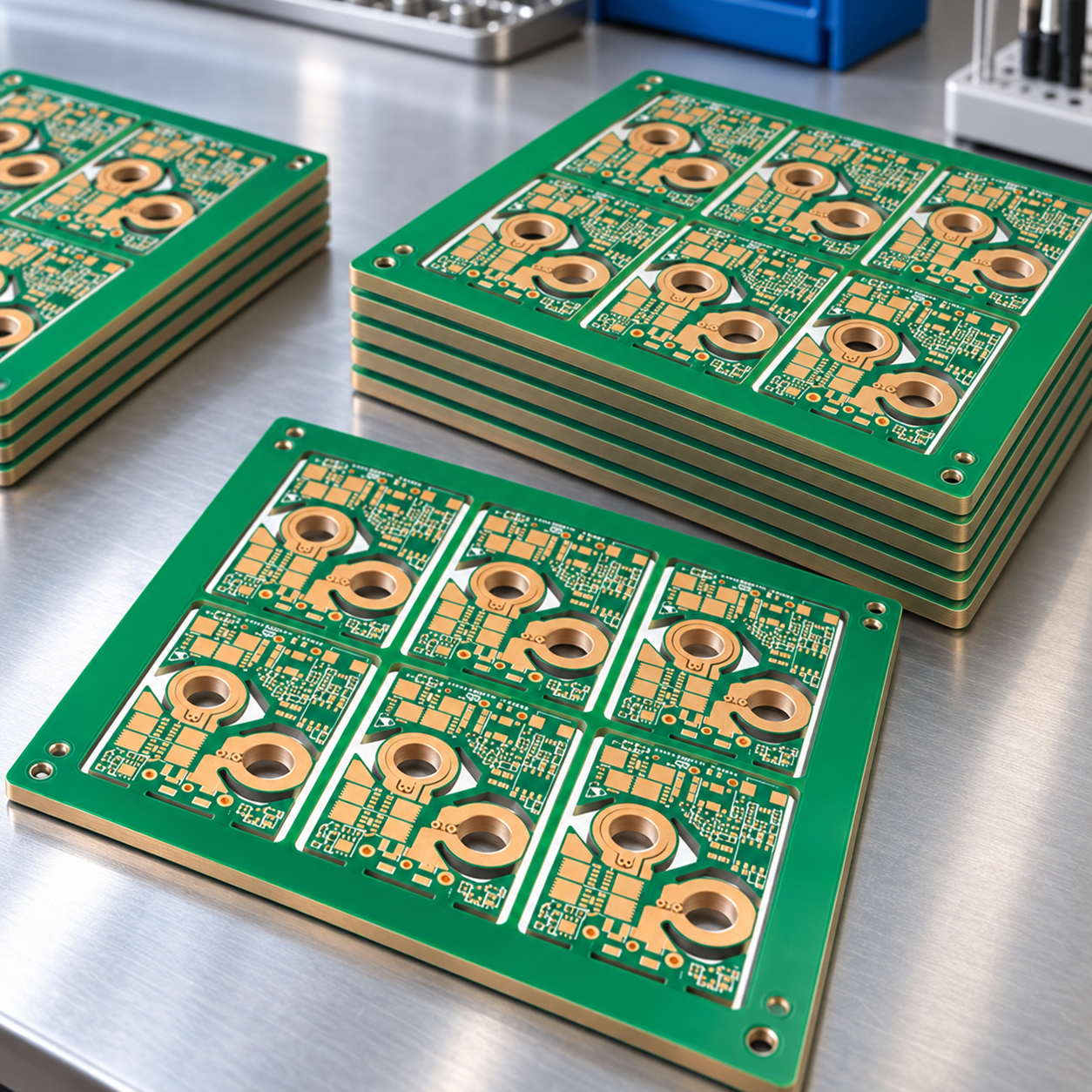
Heavy Copper PCB Manufacturers in Canada

FAQs About Heavy Copper PCB Manufacturers in Canada

Q1: Is 3 oz copper considered heavy copper?

A1: Many PCB manufacturers use 3 oz copper or more as the starting point for heavy copper, although the exact definition can vary. The fabrication drawing should state the required finished copper rather than relying only on a product-category label.

Q2: Should copper thickness be specified in ounces or microns?

A2: Either unit is acceptable if the requirement is clear. More importantly, specify whether the value refers to base copper or finished copper and identify the requirement for each layer.

Q3: Can standard copper and heavy copper be used in the same multilayer PCB?

A3: Yes. Mixed-copper stackups are possible, but copper balance, resin fill, dielectric thickness, and lamination should be reviewed as one complete construction.

Q4: When is a microsection coupon worth requesting?

A4: A microsection coupon is useful when plated-hole copper, internal-layer connections, dielectric condition, or another cross-sectional feature requires documented verification. Define the sampling requirement before production.

Q5: Does thicker copper always reduce PCB temperature rise?

A5: No. Temperature rise also depends on current, conductor width and length, copper distribution, airflow, ambient temperature, duty cycle, and heat transfer through the assembly.

Q6: Can heavy copper PCBs use ENIG?

A6: Yes, provided ENIG is compatible with the pad geometry and assembly requirements. Include the selected surface finish in the fabrication data so every supplier quotes the same construction.

Q7: Should prototype and production boards use the same stackup?

A7: Where practical, yes. Keeping the approved material, stackup, manufacturing site, and controlled requirements consistent can reduce requalification work when the project moves into production.

Q8: Should an alternative laminate be accepted if its electrical properties are similar?

A8: Not automatically. Review the electrical, thermal, mechanical, flammability, processing, and customer-approval requirements before accepting a material substitution.

Q9: When should first-article approval be repeated?

A9: Review or repeat first-article approval after changes to the PCB revision, material, stackup, manufacturing site, or another controlled process that could affect the approved result.

Q10: What should be checked before placing a repeat order?

A10: Confirm the current revision, approved stackup, material, manufacturing site, quantity, open deviations, inspection requirements, pricing, and delivery terms. A repeated part number should not hide a changed construction or production route.

Would you like to get a heavy copper PCB quote based on your actual stackup and delivery requirements? Send your Gerber or ODB++ files, stackup, finished copper by layer, drill files, quantity, inspection requirements, and Canadian delivery destination to sales@bestpcbs.com. EBest Circuit can review the construction before quotation and provide a clear manufacturing scope, inspection basis, pricing structure, and Lead Time so you can compare the offer with fewer hidden assumptions.
You may also like

Reliable PCB Heavy Copper with Custom Design
Thursday, December 18th, 2025

PCB Heavy Copper​ refers to printed circuit boards manufactured with copper weights significantly higher than the standard 1oz or 2oz, typically starting at 3oz per square foot and extending to 20oz or more, to manage high current and intense thermal loads. This article provides a comprehensive guide to everything from the fundamentals of thick copper PCBs and their design to selecting a trustworthy manufacturer for your custom projects.

Are you struggling with these common challenges for your custom heavy copper PCB projects?

  • Thermal Failure:​ Standard PCBs overheat and fail under high power, causing premature device breakdown.
  • Current Limitations:​ Thin traces cannot carry the required amperage, leading to voltage drops, trace burnout, and fire risks.
  • Mechanical Weakness:​ Inferior boards with poor plating or lamination suffer from pad lifting, via cracking, and broken connections under thermal stress.
  • Complex Design Hurdles:​ Finding accurate heavy copper PCB design​ guidelines and reliable PCB copper weight calculator​ tools is difficult.
  • Manufacturer Capability Gap:​ Many standard circuit board manufacturers lack the specialized equipment and expertise for extreme heavy copper PCB​ fabrication, resulting in poor yield and long lead times.

The solution lies in partnering with a specialist manufacturer who masters the entire process—from custom heavy copper PCB​ design support to precision manufacturing. Here’s how we address these core issues:

  • Superior Thermal Management:​ We integrate PCB copper heatsink​ structures and use high-Tg materials to effectively dissipate heat, preventing thermal failure.
  • High-Current Carrying Capacity:​ Our expertise in heavy copper PCB manufacturing​ ensures traces and planes with low impedance, safely handling hundreds of amps.
  • Enhanced Mechanical Integrity:​ Advanced plating and controlled lamination processes create robust interconnects and strong adhesion, ensuring reliability in harsh environments.
  • Expert Design Collaboration:​ We provide clear heavy copper PCB design guidelines​ and support to navigate challenges like aspect ratios and etching tolerances for your customized heavy copper PCB.
  • Dedicated Production & Quick Turn:​ Our factory is equipped for heavy copper PCB​ production, offering professional heavy copper thickness multilayer PCB services, including quick turn heavy copper PCB​ options without compromising quality.

At BEST Technology, we are a specialized heavy copper PCB factory​ with deep expertise in fabricating reliable, high-performance boards. We combine advanced process with rigorous quality control to deliver solutions that meet the most demanding electrical and thermal requirements. For your custom heavy copper PCB circuit board​ needs, pls feel free to contact us at sales@bestpcbs.com.

PCB Heavy Copper

What Is PCB Heavy Copper?

Heavy copper PCBs are defined by their exceptional conductor thickness. While standard PCBs use 1oz (35µm) or 2oz (70µm) copper, heavy copper starts at 3oz (105µm) and can exceed 20oz (700µm). This isn’t just about thicker foil; it involves specialized processes to plate and etch these massive copper weights, often creating unique cross-sectional profiles for traces and planes.

Key Characteristics:

  • Copper Weight:​ Ranges from >3 oz/ft² to 20+ oz/ft².
  • Construction:​ Can be used on inner layers, outer layers, or both in multilayer boards.
  • Purpose:​ Primarily for high-current paths, power distribution, and thermal dissipation.
PCB Heavy Copper

How Does PCB Heavy Copper Differ From Standard PCBs?

The difference extends far beyond a simple thickness measurement, impacting design, manufacturing, and performance.

AspectStandard PCB (1-2 oz)Heavy Copper PCB (3-20+ oz)
Primary Function​Signal routing, low-power circuitsHigh-current carrying, thermal management
Trace Width/Spacing​Fine features possibleWider traces and spacing required
Thermal Performance​Moderate, relies on external heatsinksExcellent, acts as an integral PCB copper heatsink​
Mechanical Strength​StandardSuperior (stronger vias, plated holes, and substrate bond)
Manufacturing Process​Standard etching & platingSpecialized sequential lamination, plating, and differential etching
Cost​LowerHigher due to material use and complex process

In summary, heavy copper PCB boards​ are engineered solutions for power, not just carriers for signals.

What Equipment Is Required in Heavy Copper PCB Factory Production?

Producing heavy copper PCBs demands specialized machinery beyond a standard PCB line.

  • High-Capacity Plating Lines:​ Essential for electroplating thick copper layers onto hole walls and surfaces to achieve the target PCB copper weight.
  • Deep Etching Systems:​ Equipment capable of differentially etching thick copper with precise control to maintain fine tolerances on sidewalls.
  • Controlled Lamination Presses:​ High-pressure and high-temperature presses that ensure proper resin flow and bonding without voids when laminating thick copper cores.
  • Laser Direct Imaging (LDI):​ For accurately patterning thick copper-clad laminates, where standard photo tools may struggle with light penetration and sidewall reflection.
  • Advanced Drilling & Routing:​ Robust drilling machines for creating clean holes in thick copper stacks and routing tools for separating the heavy, robust panels.

How PCB Thick Copper Improves Current Carrying and Thermal Performance?

The performance benefits are rooted in fundamental physics.

First, current carrying capacity is directly related to cross-sectional area. Doubling copper thickness doubles the area for a given trace width, drastically reducing resistance (R = ρL/A). This minimizes I²R losses and voltage drop.

Second, thermal performance improves because copper is an excellent thermal conductor. A PCB thick copper​ plane acts as a distributed copper core PCB​ heatsink, spreading heat away from hot components (e.g., power MOSFETs, inductors) to the board edges or designated thermal pads.

Formula for Trace Resistance:​ R = ρ * (L / (T * W))where ρ=resistivity, L=length, T=thickness, W=width. Increasing T​ directly reduces R.

PCB Copper Weight Explained and Why It Matters in Heavy Copper Designs?

PCB copper weight​ is the mass of copper per unit area, expressed in ounces per square foot (oz/ft²). It defines the finished thickness of the copper conductor.

  • 1 oz copper:​ Means 1 oz of copper spread over a 1 sq ft area, resulting in a thickness of ~1.37 mils (0.0348 mm). 1 oz copper thickness mm​ is approximately 0.035mm.
  • 4 oz copper PCB:​ Has a copper thickness of ~5.5 mils (0.14 mm).
  • 20 oz copper PCB:​ Represents an extreme thickness of ~27.4 mils (0.7 mm).

In heavy copper PCB design, specifying the correct weight is critical. It determines the current rating, thermal mass, and mechanical requirements of the board, directly impacting safety, reliability, and size.

Heavy Copper PCB Design Guidelines for High-Current Applications

Designing a reliable PCB heavy copper with custom design​ requires adherence to specific rules to avoid manufacturing defects and ensure performance.

  • Aspect Ratio:​ Maintain a sensible drill diameter to board thickness ratio (typically < 10:1 for heavy copper) to ensure proper via plating.
  • Trace Width/Spacing:​ Use a PCB copper weight calculator​ (based on IPC-2152) to determine adequate trace width for your current. Allow for extra spacing due to etching undercut.
  • Thermal Relief:​ Always use thermal relief connections for components soldered to heavy copper planes to facilitate soldering heavy copper PCB.
  • Corner Design:​ Use 45-degree angles or rounded corners on traces to improve plating uniformity and reduce stress points.
  • Layer Transition:​ For multilayer boards, use multiple vias in parallel when connecting heavy copper layers to handle the current and reduce inductance.
  • Material Selection:​ Specify high-Tg (e.g., >170°C) and high thermal reliability materials to withstand the stresses of thick copper lamination.

Maximum PCB Copper Thickness and Practical Manufacturing Limits

The maximum PCB copper thickness continues to increase as heavy copper manufacturing technology advances. In standard PCB production, commonly used copper weights include 1 oz (35 µm), 2 oz (70 µm), 3 oz (105 µm), 4 oz (140 µm), and 6 oz (210 µm), with 1 oz copper remaining the most widely adopted option for general-purpose electronics.

For applications involving higher current loads, designers typically select 2 oz copper or thicker to reduce resistive losses and improve thermal dissipation. As current demand increases, thicker copper becomes essential to maintain electrical stability and avoid excessive temperature rise.

In contrast, high-frequency applications often favor 1 oz copper or thinner. Thinner copper helps minimize conductor loss and signal attenuation, which is critical for maintaining signal integrity at higher frequencies.

As requirements move beyond standard designs, 20 oz copper thickness in heavy copper PCB is already commercially available. Some specialized heavy copper PCB factories are capable of processing copper thicknesses of 30 oz or more by using advanced techniques such as embedded copper PCB structures, copper inlays, or pre-formed copper inserts.

However, the practical manufacturing limits of PCB heavy copper are not determined by copper weight alone. They are defined by several key process constraints:

  • Etching capability
    The ability to form controlled trace geometries without excessive undercut becomes increasingly challenging as copper thickness increases.
  • Plating uniformity
    Ensuring even copper distribution in deep vias, plated features, and across the entire panel is critical for electrical and mechanical reliability.
  • Lamination challenges
    Very thick copper layers increase the risk of resin starvation, poor adhesion, and void formation during lamination, especially in multilayer structures.

In most real-world power and industrial applications, 10 oz to 12 oz copper offers an optimal balance between current-carrying capacity, thermal performance, cost efficiency, and manufacturability. Copper thickness beyond this range is typically reserved for highly specialized designs where extreme electrical or thermal demands justify the added complexity and cost.

Heavy Copper PCB Manufacturing Process and Key Technical Challenges

The heavy copper PCB manufacturing​ process is nuanced.

  • Core Preparation:​ Starting with a thick copper-clad laminate.
  • Drilling:​ Creating holes for vias and PTHs.
  • Electroplating:​ The critical step of depositing copper to build up thickness on surfaces and in holes. This often requires multiple plating cycles.
  • Patterning & Etching:​ Using a thick, robust resist to define the circuit pattern and then chemically etching away the unwanted copper. Controlling the etch factor is a major challenge.
  • Lamination (for multilayer):​ Stacking and bonding layers. Managing the PCB copper density​ and resin flow is crucial to avoid delamination.
  • Surface Finish & Testing:​ Applying finishes like ENIG or HASL and conducting rigorous electrical and thermal tests.
  • Key Challenges:​ Avoiding plating voids, controlling sidewall profile during etching, preventing inner layer separation during lamination, and ensuring even copper distribution.

How to Check PCB Copper Thickness?

Accurate verification of PCB copper thickness is critical for quality control, electrical performance, and reliability. In practice, manufacturers and laboratories use a combination of destructive and non-destructive measurement methods, depending on accuracy requirements, board structure, and testing conditions.

Commonly used PCB copper thickness measurement methods include:

  • Cross-Sectioning (Metallographic Analysis)
    This is the most accurate and authoritative method. A PCB sample is cut, mounted, polished, and examined under a metallographic microscope or scanning electron microscope (SEM) to directly measure copper thickness. It is widely used for process validation and failure analysis.
  • X-ray Fluorescence (XRF)
    XRF is a non-destructive technique commonly used to measure surface copper plating thickness. It provides fast and accurate results for outer layers and is widely adopted in production inspection.
  • Micro-Resistance Measurement
    This method calculates copper thickness by measuring the electrical resistance of a trace with a known length and width. It is useful for estimating average copper thickness and is often applied during process monitoring.
  • Eddy Current Measurement
    Based on electromagnetic induction, eddy current testing allows non-contact and non-destructive copper thickness measurement, particularly effective for surface copper layers.
  • Weight Difference (Gravimetric Analysis)
    By weighing a panel before and after etching, manufacturers can indirectly calculate the average copper weight. This method is mainly used for process comparison and verification, rather than precise local measurement.
  • Chemical Etching and Coulometric Methods
    These techniques determine copper thickness by controlled chemical removal or electrochemical reactions. They are accurate but destructive, and typically used in laboratory environments.
  • Optical and Image-Based Measurement Systems
    High-resolution optical instruments and image measurement systems can quickly visualize and measure copper thickness, especially when combined with calibrated reference standards.
  • Ultrasonic and Laser Measurement Techniques
    These methods are applied in specific cases, such as complex multilayer boards, where non-contact measurement is required. Their effectiveness depends heavily on material structure and calibration.

To ensure reliable results, several practical considerations must be followed:

  • Samples should be cleaned and pre-treated before measurement to remove contaminants.
  • Measuring instruments must be properly calibrated prior to use.
  • Measurement points should be carefully selected to ensure representative data.
  • Environmental factors such as temperature and humidity should be controlled.
  • Multiple methods may be combined to cross-verify results, as each technique has inherent limitations.

In summary, no single method is suitable for all PCB copper thickness measurements. Cross-sectioning and XRF remain the most widely trusted techniques in the PCB industry, while electrical, electromagnetic, optical, and chemical methods provide valuable complementary data. The appropriate measurement approach should always be selected based on accuracy requirements, board structure, and inspection purpose.

What Applications Require PCB Heavy Copper Circuit Boards?

These boards are essential in high-power, high-stress industries:

  • Power Converters & Supplies:​ UPS systems, industrial SMPS, welding equipment.
  • Automotive & EV:​ Battery management systems (BMS), motor controllers, charging infrastructure.
  • Renewable Energy:​ Solar inverter combiner boxes, wind turbine control systems.
  • Industrial Equipment:​ Motor drives, high-power LED lighting, power distribution backplanes.
  • Aerospace & Defense:​ Radar systems, power distribution units (PDUs), avionics.
  • High-Voltage Applications:​ Heavy copper PCB vacuum high voltage​ equipment like X-ray generators and particle accelerators.

How Do Heavy Copper PCB Factories Control Etching and Plating Quality?

Top-tier heavy copper PCB manufacturers​ implement stringent controls:

  • Plating:​ Use pulse or periodic reverse plating for better throwing power and uniformity. Monitor bath chemistry, temperature, and current density in real-time.
  • Etching:​ Employ spray etchers with precise chemistry control and multi-stage rinsing. They carefully balance etch rate to achieve the desired heavy copper PCB thickness chart​ specifications without over-etching fine features.
  • Process Qualification:​ Running test coupons on every panel for cross-sectional analysis to validate plating thickness in holes and on surfaces.
  • Automated Optical Inspection (AOI):​ To catch etching defects like nicks, mouse bites, or insufficient copper removal.

What Is Driving Growth in the Heavy Copper PCB Market?

The heavy copper PCB market​ is expanding due to several key trends:

  • Electrification:​ The boom in EVs, charging stations, and renewable energy demands robust power electronics.
  • Miniaturization with Higher Power:​ Devices are getting smaller but more powerful, increasing power density and thermal management needs.
  • Reliability Demand:​ Industries like automotive and aerospace require longer lifespans and higher reliability under thermal cycling, which heavy copper provides.
  • Advancements in Technology:​ Improved manufacturing processes are making heavy copper PCB boards​ more accessible and cost-effective.

How to Choose a Reliable Heavy Copper PCB Manufacturer for Custom Projects?

Selecting the right partner is crucial for success. Look for:

  • Proven Expertise & Specialization:​ Seek a professional heavy copper thickness multilayer PCB manufacturer, not just a generalist. Review their portfolio for similar projects.
  • Technical Support & DFM:​ They should offer proactive heavy copper PCB design​ review and strong Design for Manufacturability (DFM) feedback.
  • Advanced Capability Portfolio:​ Can they handle your required maximum PCB copper thickness, layer count, and incorporate features like copper core PCB​ or embedded copper?
  • Transparent Communication & Pricing:​ They should provide clear heavy copper PCB quotes, a detailed heavy copper PCB pricelist​ breakdown, and realistic timelines.
  • Robust Quality Certifications:​ Certifications like IATF 16949 (automotive), AS9100 (aerospace), and ISO 9001 are strong indicators of a quality system.
  • Geographic Consideration:​ While there are many China heavy copper PCB manufacturers, also consider heavy copper PCB USA​ or heavy copper PCB UK​ suppliers for proximity and IP protection if needed.
PCB Heavy Copper

To summarize, PCB Heavy Copper​ is an enabling technology for the most demanding power electronics, offering unmatched current capacity, thermal dissipation, and mechanical robustness. This guide has explored its design, manufacturing, applications, and selection criteria to empower your next high-power project.

For a reliable PCB heavy copper with custom design​ that meets your exact specifications and performance benchmarks, partner with a specialist. BEST Technology possesses the dedicated equipment, engineering expertise, and rigorous quality controls to deliver superior heavy copper PCB circuit boards. We support projects from prototype to volume production, including quick turn​ needs. A warm welcome to contact our team to discuss your requirements: sales@bestpcbs.com.

FAQs

How Thick Is a Heavy Copper PCB?

  • A heavy copper PCB typically refers to a printed circuit board with copper thickness greater than 3 oz (105 µm) per layer. Common heavy copper ranges include 4 oz, 6 oz, 10 oz, and in specialized applications, 20 oz or more, depending on current, thermal, and mechanical requirements.

What Type of Copper Is Used in PCBs?

  • Most PCBs use electro-deposited (ED) copper foil, which is well suited for standard and heavy copper applications. For high-frequency or signal-sensitive designs, rolled annealed (RA) copper may be used due to its smoother surface and better flexibility, especially in flex and rigid-flex PCBs.

How Thick Is 1 oz Copper on a PCB?

  • 1 oz copper on a PCB has a nominal thickness of approximately 35 µm (0.035 mm). This is the most commonly used copper thickness for standard PCBs and is suitable for general signal and low-current applications.

How Thick Is 3 oz of Copper on a PCB?

  • 3 oz copper corresponds to a thickness of approximately 105 µm (0.105 mm). It is often used in designs that require higher current capacity or improved thermal performance compared to standard 1 oz or 2 oz copper.

How to Choose PCB Copper Thickness?

  • PCB copper thickness should be selected based on several key factors, including current requirements, thermal dissipation needs, signal frequency, board size, and manufacturing capability. Thicker copper is typically chosen for high-current or power electronics, while thinner copper is preferred for high-frequency signal integrity and fine-line routing.

What Is the Average Thickness of a PCB?

  • The average thickness of a PCB is usually around 1.6 mm, which is the industry standard for most applications. However, PCB thickness can vary widely depending on layer count, material selection, and application requirements, ranging from less than 1.0 mm to over 3.2 mm.

You may also like