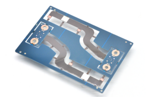
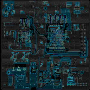
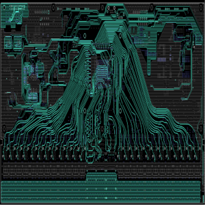
A GPU PCB connects the graphics processor, memory, power stages, PCIe interface and display section inside a graphics card. It must carry high current, route fast signals and spread heat from a compact area.
A strong board improves voltage stability, signal quality, cooling performance and long-term reliability. This guide explains the structure, working method, layout rules, thermal control, mechanical risks, manufacturing process and safe cleaning method.
What Is a GPU PCB?
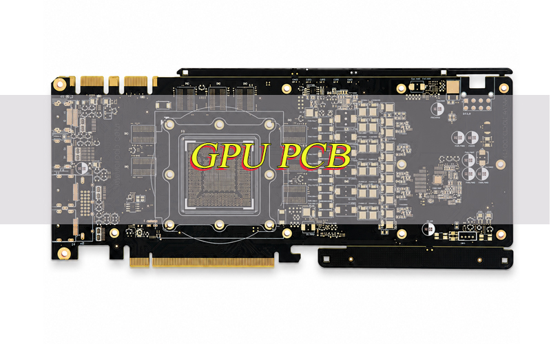
A GPU PCB is a printed circuit board made for a graphics processing unit and its support circuits. The GPU chip handles graphics and parallel computing tasks, while the board delivers power, connects memory, routes signals and supports cooling hardware.
It is not the full graphics card. A graphics card includes the PCB, GPU chip, VRAM, VRM, cooler, fan, bracket, firmware and housing parts. The board is the electrical base that allows these parts to work together.
Its main role is stable power delivery, clean signal routing, heat spreading and mechanical support. If the board structure is weak, the card may show crashes, artifacts, overheating, warping or shorter service life.
What Are the Main GPU PCB Components?
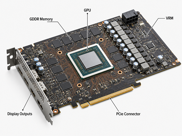
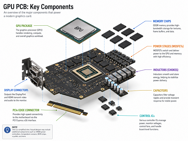
The main GPU PCB components include the GPU chip, VRAM, VRM, MOSFET or DrMOS power stages, inductors, capacitors, PCIe edge connector, auxiliary power connector, BIOS chip, clock circuit, display circuit and sensors. These parts work together for processing, memory access, voltage control, signal transfer and protection.
| Part | Function |
|---|---|
| GPU Chip | Graphics and parallel computing |
| VRAM | High-speed graphics memory |
| VRM | Voltage conversion for GPU and memory |
| MOSFET / DrMOS | Current switching in power stages |
| Inductor | Current smoothing |
| Capacitor | Ripple reduction and power stability |
| PCIe Edge | Motherboard connection |
| Power Connector | Extra power input |
| BIOS Chip | Firmware storage |
| Clock Circuit | Timing signal support |
| Sensor | Temperature and voltage reading |
| Display Circuit | Video signal path |
This table is accurate for most modern graphics cards. Some boards may combine power parts into integrated power stages, while some high-power cards may add more controllers, sensors or protection circuits.
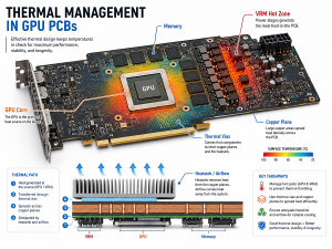
The GPU, VRAM and VRM sections carry the highest electrical and thermal load. For inspection or failure analysis, these areas should be checked first because burn marks, cracked solder joints, loose inductors and damaged connectors often appear near power and memory circuits.
What Materials Are Used in a GPU PCB?
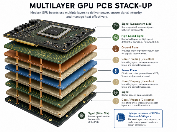
A GPU PCB commonly uses high-Tg FR-4, low-loss laminate, copper foil, prepreg, core material, solder mask, plated vias and surface finish. These materials affect signal loss, soldering reliability, heat resistance and board flatness.
| Material | Use |
|---|---|
| High-Tg FR-4 | Multilayer board base |
| Low-Loss Laminate | Faster signal routing |
| Copper Foil | Power, ground and signal paths |
| Prepreg | Layer bonding |
| Core | Layer structure support |
| Solder Mask | Copper protection |
| Plated Via | Interlayer connection |
| ENIG | Flat solderable finish |
| OSP | Lower-cost solderable finish |
This material table is accurate for general graphics board production. High-performance boards often use better dielectric control, heavier copper and more stable laminate to support high current and fast signal transmission.
ENIG is common when flat pads, storage stability and fine-pitch assembly matter. OSP may be used in cost-controlled projects when assembly timing is well managed. Material selection should match power level, signal speed, layer count and soldering temperature.
Weak laminate stability can increase warpage, signal loss and reliability risk after repeated heating. For this reason, board material should be confirmed before layout approval, not after sample failure.
How Does a GPU PCB Work?
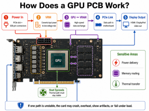
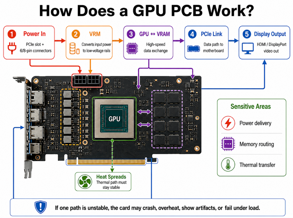
A GPU PCB works by moving power and data between the graphics processor, VRAM, motherboard and display circuits. Power enters through the PCIe slot and auxiliary connectors, then the VRM converts it into low-voltage rails.
The GPU exchanges data with VRAM through short high-speed routes. PCIe lanes connect the board to the motherboard, while display circuits send video signals to HDMI, DisplayPort or other ports.
The working path is direct: power enters, voltage is regulated, data moves, heat spreads and video leaves the card. If one path is unstable, the card may crash, overheat, show artifacts or fail during load testing.
The most sensitive areas are power delivery, memory routing and thermal transfer. A small voltage drop, poor return path or weak heat path can affect the whole graphics card.
How to Read a GPU PCB Diagram and Schematic?
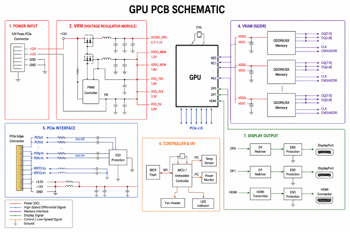
Read the GPU PCB diagram and schematic by separating the board into physical zones and electrical circuits. The diagram shows where parts sit, while the schematic shows how power and signals move.
- Find the GPU area first. The GPU chip is usually near the center, with VRAM placed close around it to shorten memory routes and reduce timing mismatch.
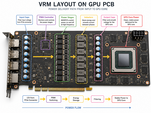
- Locate the power section. VRM stages, inductors and capacitors are usually near the power input or along one side of the board.
- Check the PCIe path. PCIe fingers sit at the bottom edge and connect the card to the motherboard through high-speed lanes.
- Trace the display section. HDMI, DisplayPort and related protection parts are near the rear bracket.
- Follow voltage rails. Start from input power, then follow converted rails to the GPU, memory and control circuits.
- Separate signal and power areas. This makes fault reading easier and prevents confusion between high-current and high-speed routes.
The simplest reading method is to divide the board into power, memory, interface, control and thermal areas. This makes a complex board easier to understand and reduces the chance of missing important circuits.
What Should You Check Before Designing a GPU PCB?
Before planning a GPU PCB, confirm the chip package, VRAM type, power budget, board size, cooler space, layer count, copper thickness and factory process limits. The board cannot be planned from the chip alone because every support circuit affects stability.
- GPU and VRAM match: Confirm package, pinout, memory type, bus width and speed grade before routing begins.
- Power demand: Calculate GPU core power, memory power, connector current and transient load.
- Board outline: Confirm PCIe bracket, mounting holes, fan space, heatsink area and enclosure clearance.
- Layer plan: Match layer count, dielectric thickness, copper weight and impedance target.
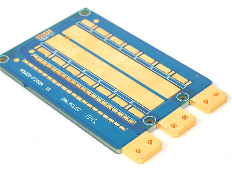
- Copper capacity: Confirm trace width, copper area and via count for high-current paths.
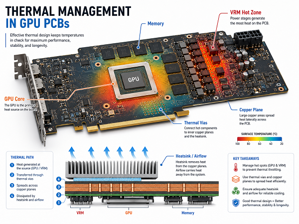
- Thermal path: Plan heat movement from GPU, VRAM and VRM to the heatsink, airflow and backplate.
- Factory limits: Check minimum trace, spacing, drill, annular ring and solder mask ability.
- Compliance target: Confirm RoHS, UL and IPC inspection needs before production.
Early checks reduce unstable samples, repeated layout changes and mass production delays. A graphics board should be designed around real electrical load, cooling space and manufacturing limits.
What Are the Best Practices for GPU PCB Layout?
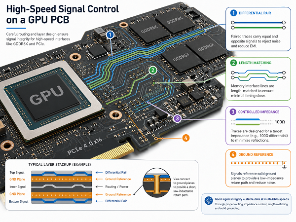
Good GPU PCB layout keeps power paths short, signal paths controlled and heat sources separated. The GPU, VRAM, VRM and PCIe areas should be arranged before smaller support circuits.
- Place VRAM close to the GPU to reduce trace length, timing mismatch and signal loss.
- Keep VRM near power input to shorten high-current paths and reduce copper loss.
- Use wide copper for power rails to reduce voltage drop and heat buildup.
- Keep solid ground under fast traces to protect return paths and reduce noise.
- Separate switching circuits from clock, sensor and signal lines.
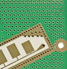
- Use via arrays under hot parts for heat transfer and current sharing.
- Balance copper distribution to reduce bending and warping during fabrication and use.
- Keep screw areas clear to prevent pressure on traces, vias and small parts.
- Reserve cooler space for thermal pads, heatsink contact and airflow movement.
A clean layout does not only place components neatly. It controls current, signal timing, heat and mechanical stress in one board.
What Are the Main GPU PCB Design Rules?
The main GPU PCB design rules cover impedance, spacing, via use, power copper, solder mask and DFM review. These rules help reduce signal reflection, voltage drop, soldering defects and low production yield.
- Control impedance for PCIe, memory and other fast signal lines.
- Match trace length where timing matters, especially around VRAM.
- Avoid broken ground planes under high-speed traces.
- Use enough vias for current sharing and thermal transfer.
- Keep high-current paths short and wide near VRM stages.
- Protect solder mask bridges between fine-pitch pads.
- Check drill size and annular ring before Gerber release.
- Reserve clearance around connectors to prevent assembly damage.
- Run DFM review before production approval.
The main rule is direct: electrical intent, layout geometry and factory capability must match before the board enters production. Ignoring this match can cause sample rework, unstable testing or poor batch consistency.
How Is a GPU PCB Manufactured?
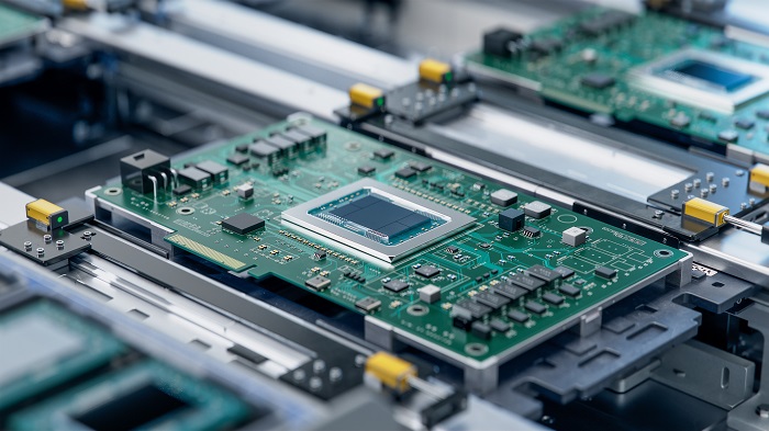
The GPU PCB manufacturing process must control layer alignment, copper thickness, via quality, solder mask registration and solderability. A small process error can affect high-speed signals, power stability or assembly yield.
Step 1: Review files and layer structure.
The factory checks Gerber files, drill data, copper weight, impedance notes, layer count and special process requirements before production. This step prevents basic file errors from entering fabrication.
Step 2: Prepare material and inner layers.
Core material is cleaned, coated, imaged and etched to form the inner copper circuits. Inner layer accuracy is important because later layers depend on this base.
Step 3: Laminate the multilayer board.
Inner layers, prepreg and copper foil are pressed under heat and pressure to form a solid board structure. Lamination must control alignment, resin flow and board flatness.
Step 4: Drill and plate holes.
Mechanical drilling or laser drilling creates vias and holes. Copper plating then connects the required layers and supports current flow between layers.
Step 5: Form outer circuits.
The outer copper layers are imaged, plated and etched to create the final trace patterns. Fine spacing, annular ring and copper thickness must be controlled carefully.
Step 6: Apply solder mask and surface finish.
Solder mask protects copper and helps prevent solder bridging. ENIG, OSP or another surface finish prepares pads for assembly.
Step 7: Route, inspect and test.
The board is cut to shape, inspected for defects and electrically tested before shipment or assembly. This step helps confirm opens, shorts and basic circuit continuity.
For assembled boards, SMT placement, reflow soldering, X-ray review, functional testing and thermal checks may follow. The final goal is stable power delivery, clean signal paths and repeatable batch quality.
GPU PCB vs CPU PCB: What Is the Difference?
A GPU PCB supports a graphics processor, on-board VRAM, local power stages and display circuits. A CPU PCB area usually belongs to a motherboard or processor module and connects the CPU to memory slots, chipset, VRM and system I/O.
| Item | GPU PCB | CPU PCB Area |
|---|---|---|
| Main Chip | Graphics processor | Central processor |
| Memory | On-board VRAM | DIMM or soldered memory |
| Interface | PCIe edge | Socket or board bus |
| Power Zone | Local VRM on card | Motherboard VRM area |
| Heat Source | GPU, VRAM, VRM | CPU and VRM |
| Layout Focus | Memory, PCIe, power, cooling | Socket, memory, chipset, I/O |
| Form | Add-in card or module | Motherboard section |
The main difference is structure and density. A graphics board has tighter local routing around the chip and memory, while a CPU board area is part of a wider system platform.
A graphics board also faces stronger local heat concentration because the processor, memory and power stages are close together. This makes copper planning, airflow and mechanical support more important.
How to Clean a GPU PCB Safely?
Cleaning a GPU PCB must be done with power removed and the board fully discharged. It is suitable for dust, light flux residue and minor surface contamination, but not for burnt copper, broken traces or deep corrosion.
Step 1: Disconnect all power.
Remove the card from the system and avoid touching contacts with bare hands. This prevents short circuits and reduces static damage risk.
Step 2: Inspect the board first.
Check for burnt marks, corrosion, loose parts, cracked solder joints and damaged connectors. Do not clean blindly if the board has visible damage.
Step 3: Remove dry dust.
Use clean air or a soft ESD-safe brush. Do not scrape the solder mask, small capacitors, resistors or connector pins.
Step 4: Clean light residue.
Apply high-purity isopropyl alcohol to a lint-free swab or soft brush, then wipe gently. Avoid flooding connectors or areas under large chips.
Step 5: Handle corrosion carefully.
White, green or black marks may indicate copper or solder damage. Do not power the board until residue and moisture are cleared.
Step 6: Dry fully before testing.
Let the board dry completely, especially around connectors, vias and fine-pitch parts. Moisture left under components can cause leakage current or shorts.
If corrosion reaches vias, connectors or BGA areas, cleaning alone may not restore reliability. Deep corrosion, cracked copper and burnt pads require inspection before reuse.
FAQs About GPU PCB
Q1: What does a GPU PCB components diagram show?
A1: A GPU PCB components diagram shows where the GPU chip, VRAM, VRM, PCIe connector, power connector and display circuits sit on the board. It helps identify power, memory, interface and thermal areas before inspection or layout review.
Q2: How is a GPU PCB schematic different from a diagram?
A2: A diagram shows the physical board layout, while a schematic shows electrical connections. The schematic is better for tracing power rails, signals and control circuits, while the diagram is better for finding parts and checking board zones.
Q3: What causes GPU PCB bending?
A3: GPU PCB bending usually comes from heavy heatsinks, long board length, weak backplate support, uneven screw pressure or poor handling. Repeated heat and load can weaken solder joints over time, especially near BGA packages and PCIe fingers.
Q4: Can a GPU PCB bent problem damage the card?
A4: Yes. A slight bend may still work, but strong or long-term bending can stress solder joints, vias, connectors and internal copper. If the board has cracks, loose parts or unstable video display, it should be inspected before use.
Q5: What causes a GPU cracked PCB?
A5: Cracks can come from drops, excessive cooler pressure, board flex, shipping damage or forced installation. Cracks near PCIe fingers, VRAM routes, power planes or BGA areas are serious because hidden internal layers may also be damaged.
Q6: Can GPU PCB repair restore full reliability?
A6: Repair can sometimes fix pads, connectors or visible traces, but it may not restore inner-layer damage or stressed BGA joints. For critical products, replacement or new production is safer than uncertain repair.
Q7: What affects GPU PCB layers count?
A7: Layer count depends on memory bus width, PCIe speed, power density, impedance control and board size. Many graphics boards use 6 to 16+ layers, while advanced boards may need more planes for power, ground and dense routing.
Q8: Is GPU PCB layout different from a normal PCB?
A8: Yes. GPU PCB layout has denser memory routing, higher current paths, stricter thermal control and tighter mechanical limits. The GPU, VRAM, VRM and PCIe areas must be planned together, not handled as separate sections.
Q9: What should be checked before custom GPU PCB production?
A9: Check Gerber files, drill files, BOM, layer details, impedance notes, copper weight, test needs and assembly drawings. Clear files reduce sampling delays, production errors and cost changes during fabrication.
Q10: What increases graphics board manufacturing cost?
A10: Cost rises with higher layer count, thicker copper, low-loss laminate, blind vias, buried vias, fine spacing, impedance control and strict inspection. Layer structure and test requirements often affect price more than board size alone.
Conclusion
A GPU PCB must handle high-speed signals, heavy current, heat and mechanical stress in a compact structure. The core technical point is clear: material, layer structure, layout, thermal path, solder quality and inspection must work together.
For project planning, focus on power capacity, controlled routing, copper weight, heat path, material stability and factory process capability before sample approval. For sourcing, compare more than unit price. Review DFM support, PCB fabrication ability, PCBA assembly quality, testing process, traceability and global delivery experience.
EBest Circuit is a China source factory supporting custom PCB and PCBA services for global projects. Send your board files, drawings or project details to sales@bestpcbs.com for quotation and manufacturing review.