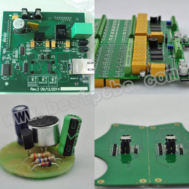
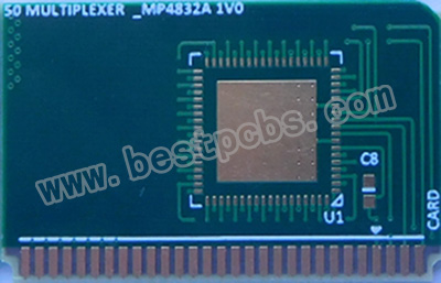
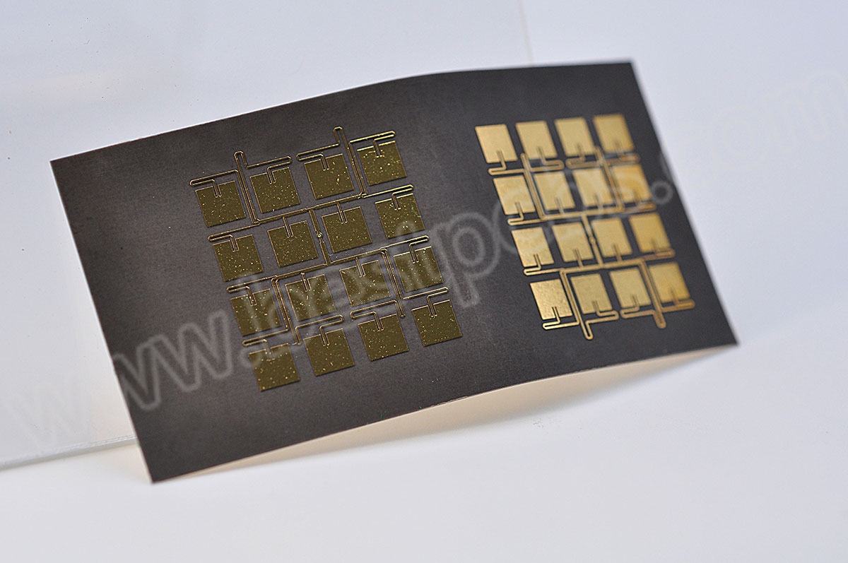
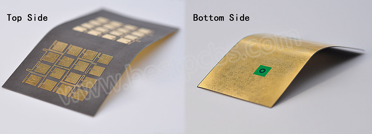
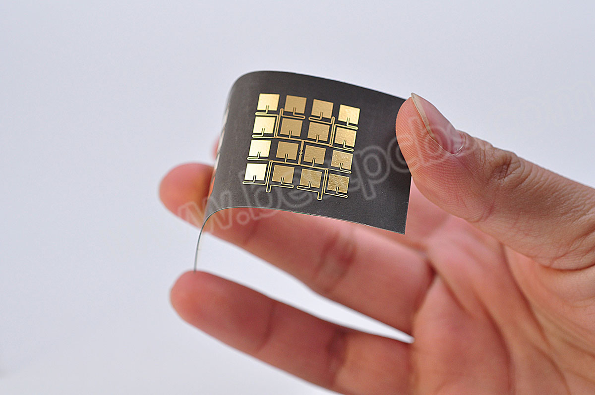
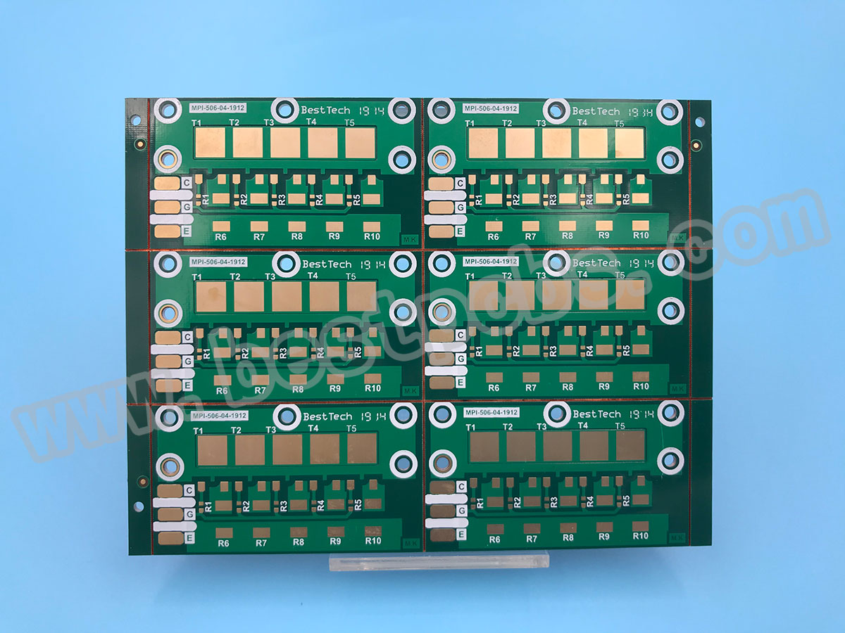
Every printed circuit board need to do full test before ship to our customer. but you may have doubt, the PCB was made according to the original Gerber file, why finish the PCB production process, why the short Circuit will occur on a FR4 circuit board?
A short circuit may also occur during reflow soldering. the solder paste may accidentally connect two pins that are very close to each other. In some cases, errors can occur during the PCB design process because the wiring between different networks accidentally connects.
We believe every PCB manufacture have their own test method to do short circuit, but today I would like share how EBest Circuit (Best Technology) to Check for Short Circuits in a Printed circuit board.
Here are some important steps:
Step 1 Visual inspection
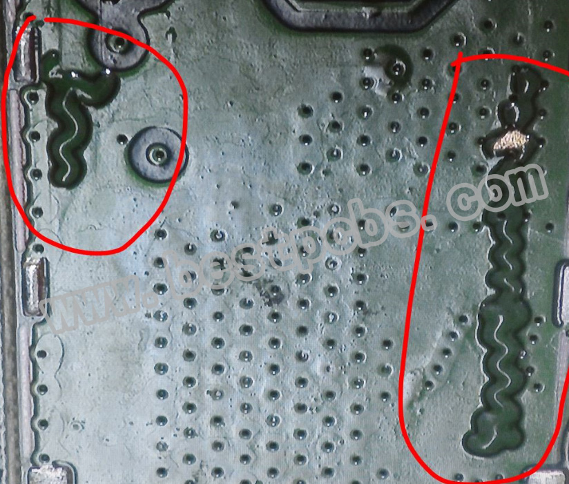
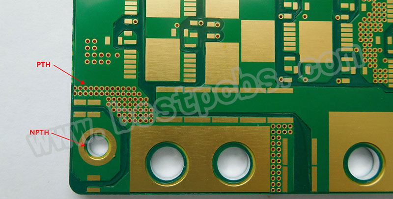
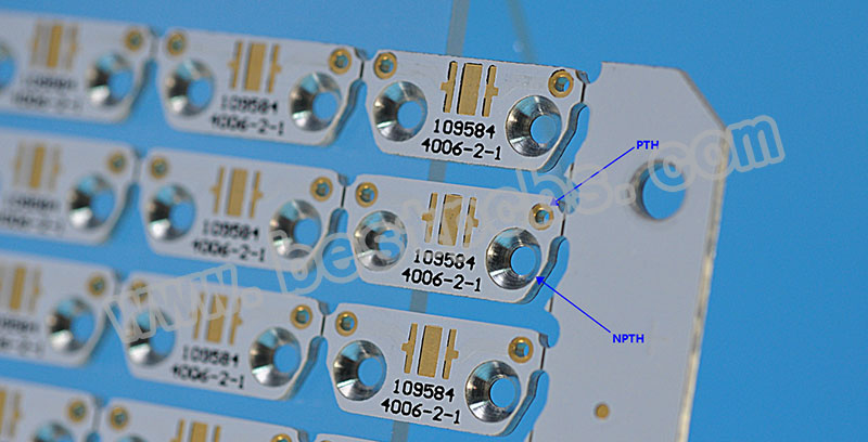
The first step for locating short circuits on PCB is to carefully look at the entire surface of the PCB. EBest Circuit (Best Technology) QC guys use a magnifying glass or low magnification microscope during the circuit board examination. We check the whole board surface to see if there are some traces break off. Any cracks or blobs of solder should get careful attention. Check all your vias. If you specified unplated vias, make sure that’s the case on the board. Poorly plated vias can create a short circuit between layers and leave you with everything tied to ground, VCC, or both.
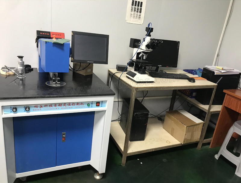
All the testing work will carry out according to IPC 6012 class 2.
Step 2 Use a Digital Multimeter to find out where is the problem
To test a circuit board for a short circuit, you need to check the resistance between different points in the circuit. If visual inspection doesn’t reveal any clues as to the location or cause of the short circuit, grab a multimeter and try to track down the physical location on the printed circuit board. The multimeter approach gets mixed reviews in most electronics forums, but tracing your test points can help you figure out what isn’t the problem.
Step 3 use Probe flying Tester &E-tester
As long as you are in Printed Circuit board field, you are definitely known Probe flying test and E-Teter.
Flying probe test systems require no test fixture, it can serve both prototype and small production, providing maximum flexibility for PCB manufacturers and this job can complete in a short time.
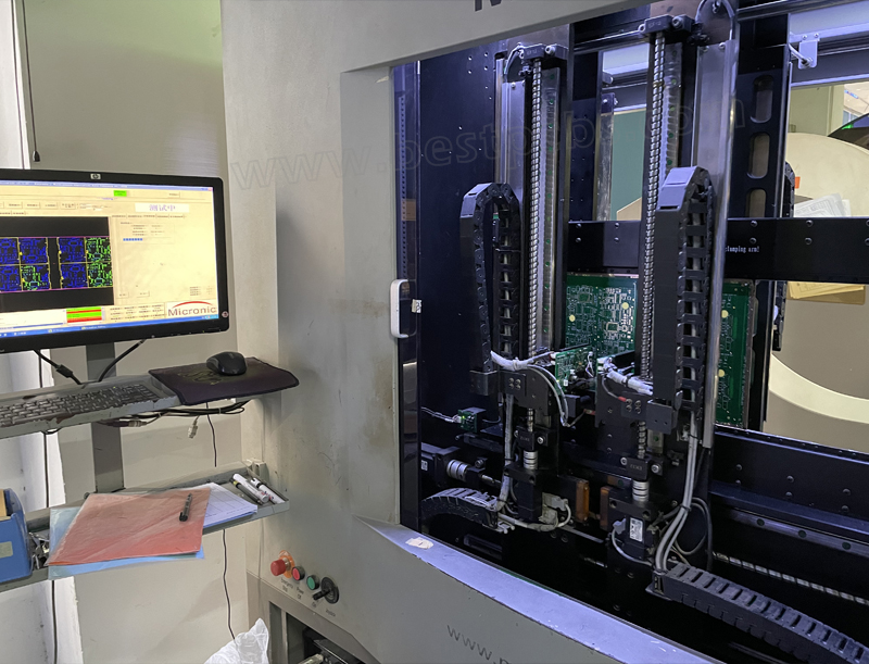
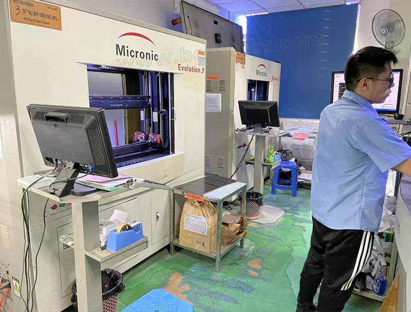
But when your circuit board become to volume, you will need to open a test tooling/test fixture to test the Printed Circuit board to test the open short circuit.
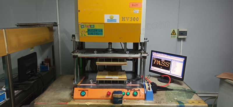
In my next blog in June, I will introduce Probe flying test to you in more detail.
If you have any question about printed circuit board, you are welcome to contact EBest Circuit (Best Technology).
It is our great pleasure to communicate with you for any issue for printed circuit boards.


.JPG)