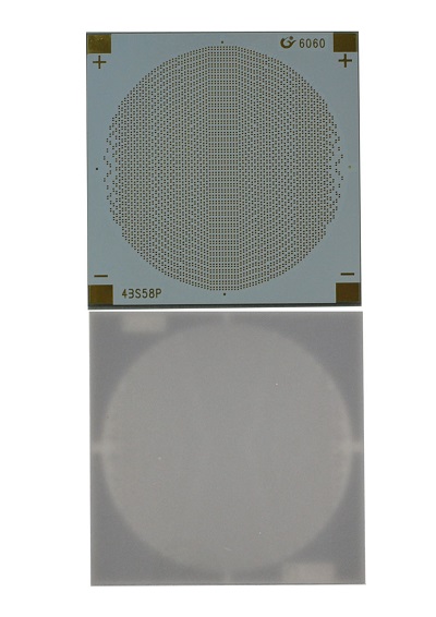
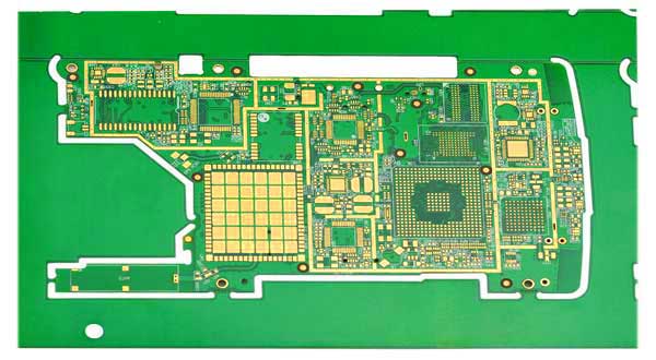
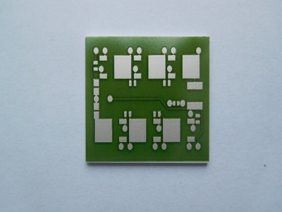
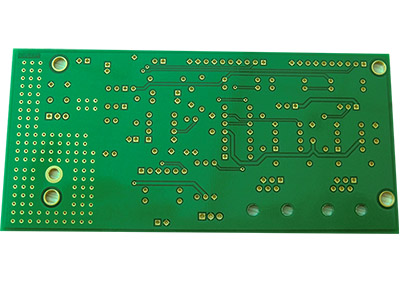
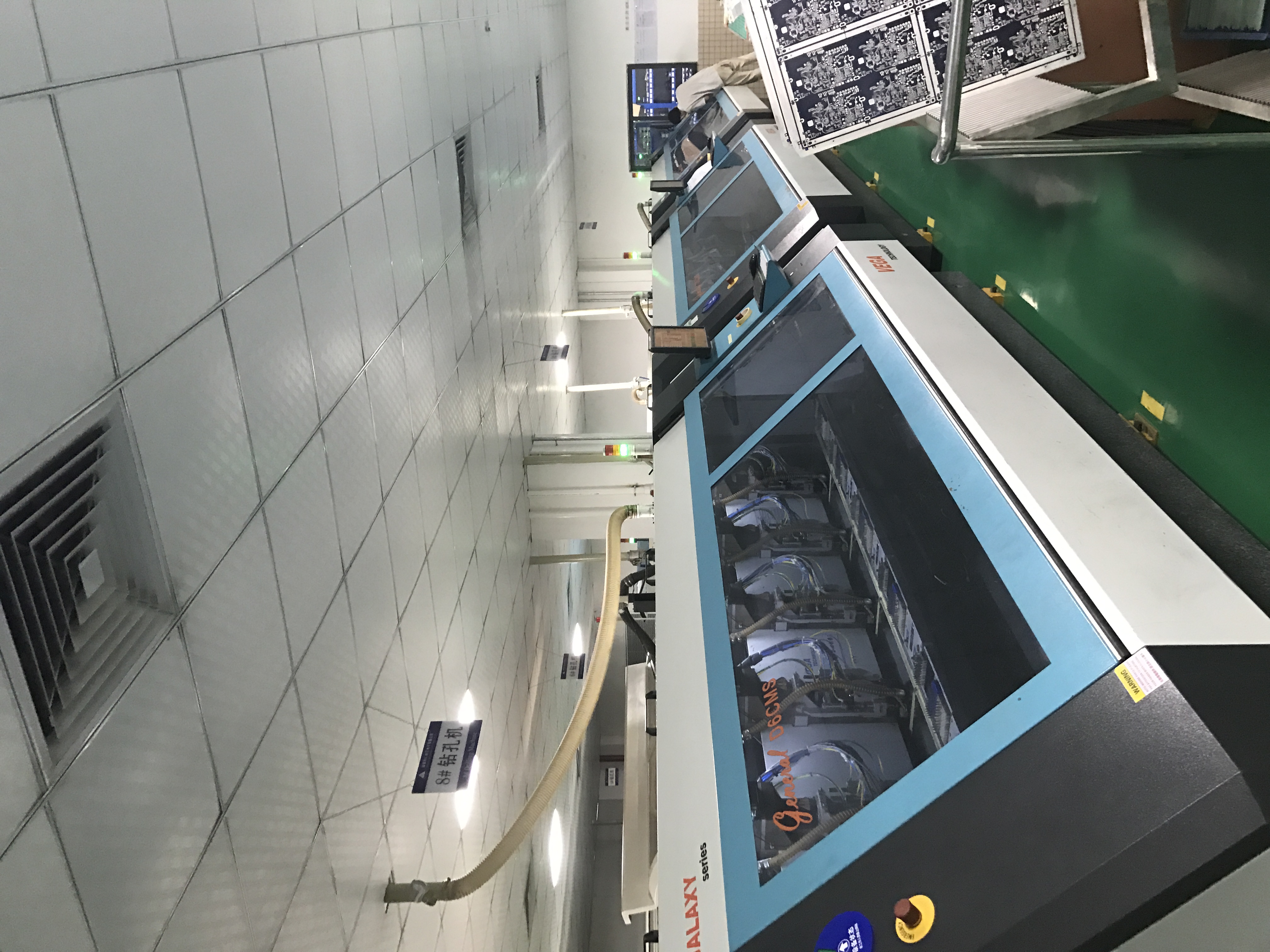
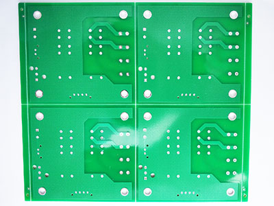
PCB manufacturing PCB manufacturing
Home > Blog

Soldermask on Hole (Via) Without Opening

October 6th, 2016

Soldermask opening always is a very important thing for various PCB, esp. for rigid FR4 PCB. In previous article, we already discussed why soldermask opening & tented was not the same like original gerber file.

If you really want soldermask opening for hole (Via) less than 0.60mm, you should added special notice when placing order.

At the same time, there’s another method you can use: To increase the soldermask opening diameter, that means add an “Annular Ringâ€Â. Normally you will need to increase 0.10mm (4mil) on each side, so that there’ll be a 0.1mm “Annular Ring†around the hole/Via, that Annual ring will stop soldermask into the hole/via of PCB.

Because in a lot of design, if there’s Via/Hole, there’ll no opening in its soldermask file, maybe engineer think the drill will remove the soldermask and then there’ll no soldermask on these Via/hole of board. As mentioned before, if Via/Hole in Printed circuit board was less than 0.6mm, or around 0.65mm then it’ll be a problem.

See from bellowing pictures of PCB board:

0.635mm Drill hole (Via)

0.635mm Drill hole (Via)

(0.635mm Drill hole (Via)

This is the original PCB Gerber file, the diameter of drill hole was 0.635mm and there’s no soldermask opening on GTS (top soldermask) Gerber file. (Purple color was GTS, Yellow: GTL (top layer); Blue: Drill (PTH) file), and no Annular Ring.

So final circuit boards will be like belowing:

0.635mm Via covered/tented by soldermask

0.635mm Via covered/tented by soldermask


So you need to add at least 0.10mm (4mil) soldermask opening on each side of hole, so that there’ll be a 0.1mm Annular Ring, like bellowing:

Add 4mil Annular Ring on PCB Via

Add 4mil Annular Ring on PCB Via


Then that hole will become like bellowing:

Hole/Via without soldermask (soldermask opened)

Hole/Via without soldermask (soldermask opened)


We believe there’re a lot of other handling method about that soldermask opening, please leave your comments, or contact us to discuss more about that, and believe you will be happy to receive with the PCB with correct soldermask opening!

You may also like

Why Soldermask Opening or Tented was not the same like the Original Gerber file?

August 29th, 2016

Recently customer compliant that the soldermask for some holes, esp for PTH (plated through hole, sometimes people named Via) was wrong, because in his original Gerber file, it was opened, but on actual printed circuit board, it was tented (covered), and some cases, some was tented and some was opened at the same time. It made customer confused.

In fact, there’s a default rule in PCB (printed circuit board) manufacturing: If the PTH (Via) was less than 0.60mm, then the soldermask will be made as per factory’s default rules: making them as tented (covered), regardless it was tented or opened in customers’ original Gerber file.

Here you can see pictures showing a board with a 0.30mm PTH, soldermask was opened in original Gerber file, but in real board, it was tented.

0.3mm Via soldermask

0.3mm Via soldermask

And in this board, for 0.508mm PTH (via), some soldermask was opened and some was opened.

0.508mm Via soldermask

0.508mm Via soldermask

Why like that? Here are two major reasons:

1) For PTH(via) less than 0.6mm, normally the function was only to electrically connected trace, not for electronic components assembled; so whatever PTH was opened or tented, it doesn’t matter.
2) In rigid printed circuit board manufacturing, it’s not easy to etch away the soldermask around PTH less than 0.60mm. As soldermask was made by that method: printed whole area with oil (soldermask), then undergo develop & exposure, then pass the etching line. The chemical will etch away the oil accordingly to the drawing, but if the hole was too small (less than 0.60mm), then the oil around will be very difficult to etch away, so you will see some oil was etched away (soldermask opened), some oil still here (soldermask tented)

If diameter of hole was bigger than 0.60mm, then it’ll be easy to etch away and some of them will be used in assembly, so we will make according to Gerber file and you will see the board exactly like the drawing. See bellowing a picture showing a board with 0.889mm (0.035mil) PTH.

0.889mm Via soldermask opening

0.889mm Via soldermask opening

Sometimes, people just use these hole as testing point, not for assembly, then we suggest to add another PAD connected to this hole so that you can test it easy. To tested on hole was not stable as tested on a PAD.

In a conclusion, in future, if the hole was less than 0.60mm and you really want it to be opened, please add special notes when release order, and allow us to enlarge the opening diameter of soldermask (around 0.60mm) so that soldermask of these holes will be opened.

Please contact us if still any question about soldermask opening.

You may also like

What will cause the solder mask layer blister and fall off?

April 8th, 2016

Some customers may get PCB that includes blister on the solder mask layer, even the solder mask layer  fall off. As PCB manufacturer, we will let you know what cause it and how to prevent on PCB manufacturing process. Please read the following information but don’t hesitate to contact us if you need more help.

  • The surface of copper is not clean and oxidation in previous processing. It need to strength the surface finishing of the boards and ensure to dry off the boards in previous processing.
  • The film was underexposed. It need to determinate and adjust the exposure energy of the boards.
  • The insufficient curing. It need to to check the heat uniformity of the dryer oven and control the curing temperature and time of boards.
  • Improper proportion of boards’ink. Pay more attention to the ink’s proportion when mixed.


You may also like

What’s the counterbore and countersink?

March 26th, 2016

Somebody may not know the different between counterbore and countersink on PCB.

Both are used to mount nails to keep the PCB in the suitble position.

The cross-section of the counterbore looks like letter “T”, but the countersink looks like a funnel.

Pls see the below picture:

PCB counterbore

PCB counterbore

PCB countersink

PCB countersink

Pls visit our website if you have more questions about PCB.

You may also like

What’s Single Layer PCB?

March 25th, 2016

Normally PCB which only one conductor is single layer PCB. Common conductor are copper , AgPd (Silver Palladium) AuPd (Gold Palladium ), Al(aluminum). Normally, for FR4 PCB, metal core PCB and Flexible PCB, the conductor are copper. For ceramic PCB, the conductor can be copper, AgPd and Aupd. Here some common structures for your reference.

single side FR4 PCB

single side FR4 PCB

single side ceramic PCB

single side ceramic PCB

Of course, there are some special circumstances, even only one conductor, but they are not single layer PCB, they are named Dual Access PCB.
For example:

dual access FR4 PCB

dual access FR4 PCB


You may also like

MCPCB can be without solder mask?

March 25th, 2016

MCPCB can be without solder mask

Yes, we can make the MCPCB without solder mask! How to do MCPCB without solder mask?


  • First step, we use our dielectric layer and laminate with copper, so we get the material of this stack up

Top: copper foil

Middle: dielectric layer

Bottom: Aluminum or Copper or Iron substrate


  • Second step, etch copper to get the trace, the areas without trace will expose the dielectric layer, the color of 1W/m.K & 2W/m.K raw material is white, 3W/m.K is light blue.


3 w m/k dielectric layer is light blue

3 w m/k dielectric layer is light blue

2 w m/k dielectric layer is white

2 w m/k dielectric layer is white

  • Third step, do the surface finish, HAL-LF, OSP, ENIG, etc…,here you will kow for no Soldermask ,it have to do surface finishing for all circuits,so if you would like to protect parts of circuits layer and which don’t need do surface finishing.

MCPCB without solder mask have no bad influent the function of the board, so solder mask with or without, only depends on your requirement.please visit for metal core PCB if you would like to know more.

You may also like

What’s the halogen-free copper clad materials

March 25th, 2016

According to the JPCA – ES – 01-2003 standard: chlorine (C1), bromine (Br) is less than 0.09% Wt (weight ratio) of the copper clad, defined as halogen-free copper clad. (at the same time, the CI + Br total less than 0.15%  [1500 parts per million])  Most of the halogen free materials are mainly composed of phosphorus and phosphorus nitrogen.when the phosphorus resin burning, it will thermal decomposition by heating and generate partial poly phosphoric acid,the partial poly phosphoric acid have strong dehydration property to come into being the carbon film on the surface of the high polymer resin,to insulated resin burning surface is exposed to air, that the fire is extinguished, flame retardant effect.

You may also like

What’s the meaning for S/M in PCB?

March 25th, 2016

S/M means solder mask, it is a kind of the Liquid photosensitive ink, it is the green, yellow, red, black or white color on PCB surface. We print solder mask on the PCB surface that no need soldering, and then drying and curing.

With solder mask, the Tin won’t stick to the PCB.

You may also like

The advantage and disadvantage of aluminum PCB

March 18th, 2016

The aluminum PCB is a unique metal base copper clad laminate , it has good thermal conductivity, electrical insulation properties and machining property.

The structure of aluminum PCB is divided into three layers.

First layer: base layer, it is the metal substrate, which can choose copper or aluminum.

Second layer: dielectric Layer, its thickness be from 0.003 inch to 0.006 inch.

Third layer: circuit layer, the copper thickness of the circuit is from 1oz to 10oz.

The advantage of aluminum PCB:

  • it has good heat radiation and better strength.


The disadvantage of aluminum PCB:

  • High cost.
  • The current mainstream can only do single aluminum PCB, it is difficult to do double sided aluminum PCB.
  • The product will be more easily to have matter in electrical strength and pressure.

Aluminum core PCB have good thermal conductivity but Ceramic PCB will better,if you would like to know more about the different from FR4,MCPCB and Ceramic PCB,pls visit to for more information.


You may also like

Company PCB & SMT Video Online Now!

October 25th, 2015

Good news! Our company Video of PCB & SMT was online now!  You can see our team member, facility, production capability (includes FR4 PCB, Metal Core PCB, Ceramic PCB, Flexible Circuit, SMT (PCBA), to see how we continue to improve ourselves, to provide best service to our customers.

Please watch the following video on YouTuBe if you cannot open the above video.

Remember EBest Circuit (Best Technology) will be your best choice of printed circuit board, most reliable partner in China!

Welcome to contact us today for more inquiries of various circuit boards.

You may also like