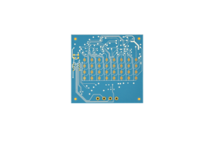
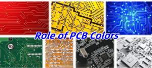
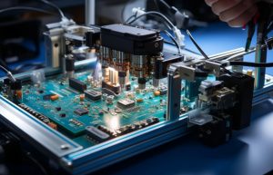
PCB manufacturing PCB manufacturing
Home > Blog

What is PCB on PCB Stacking Technology? | EBest Circuit

March 11th, 2026

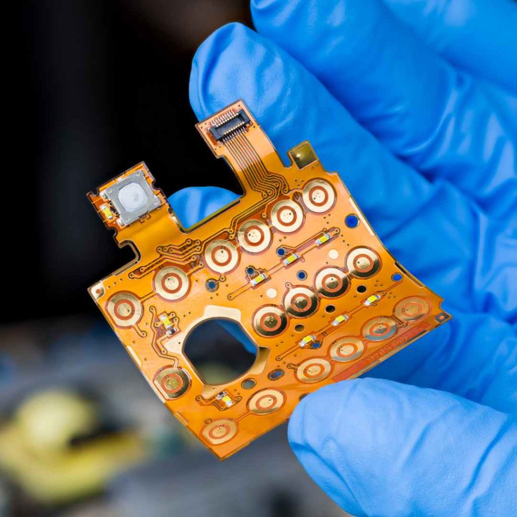
As electronic products continue to shrink in size while increasing in functionality, engineers often need to integrate multiple circuit boards into a compact system. One common approach is PCB on PCB design, where one printed circuit board is stacked or connected directly on top of another.

This architecture allows designers to build modular systems, reduce footprint, and simplify product upgrades. However, designing a reliable PCB on PCB structure requires careful consideration of connectors, mechanical support, signal integrity, and assembly processes.

In this guide, we will explore how PCB stacking works, how engineers connect two PCBs together, and what design practices help ensure long-term reliability.

What Is PCB on PCB?

PCB on PCB refers to a structure where two or more printed circuit boards are connected directly together to form a layered electronic system. Each board usually performs a specific function. When combined, they operate as a complete device.

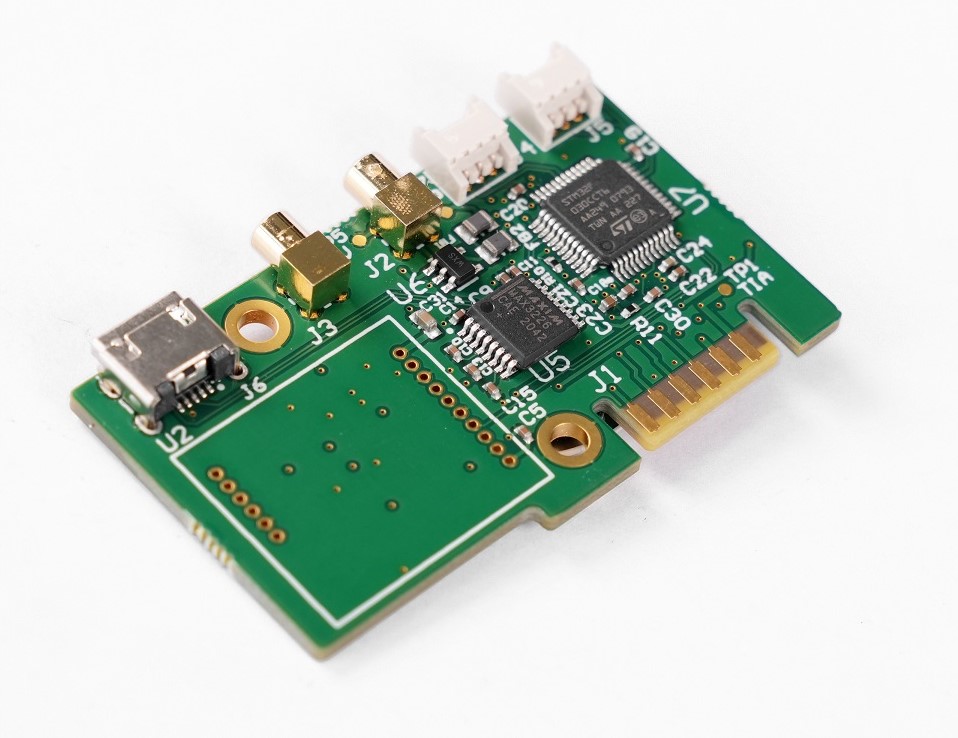
One board typically acts as the main board (motherboard). It contains the processor, power management, or key control circuits. The secondary board is often called a daughter board. This smaller board provides additional features such as sensors, wireless communication modules, or signal conversion circuits.

The connection between boards allows signals, power, and control data to travel between them. Instead of using long cables, engineers prefer direct board-to-board connections, which improve signal stability and reduce noise.

What Is PCB on PCB?

Typical PCB on PCB Structure

A typical PCB on PCB structure works through the following process:

  1. The primary board contains the core system circuits.
  2. Secondary boards add specialized functions.
  3. Electrical connectors or stacking structures link the boards.
  4. Signals transfer through dedicated connectors or pin interfaces.

This modular approach offers several advantages:

  • Compact electronic design
  • Easier upgrades or maintenance
  • Flexible system expansion
  • Improved manufacturing efficiency

Many advanced electronics rely on this architecture because it allows designers to isolate different functions while maintaining system integration.

Why Do Engineers Use PCB on PCB Designs?

Engineers often adopt PCB on PCB architectures when designing compact or modular electronic systems. The most important advantage is space optimization. By stacking boards vertically, designers can integrate more functionality within a limited enclosure. Other reasons include:

1. Modular system design

    Different functions can be separated into individual boards. For example, RF circuits, power modules, and control logic can each be placed on dedicated PCBs.

    2. Easier product upgrades

    Manufacturers can update one module without redesigning the whole board.

    3. Reduced design complexity

    Complex circuits can be divided into manageable sections.

    4. Improved manufacturing flexibility

    Some modules can be produced or tested separately before final assembly.

    Because of these benefits, PCB stacking design is widely used in telecommunications equipment, embedded systems, robotics, and IoT devices.

    Why Do Engineers Use PCB on PCB Designs?

    How to Connect Two PCBs Together?

    When engineers search how to connect PCB to PCB, they usually refer to the physical and electrical methods used to link two circuit boards. Several techniques are commonly used in industry.

    1. Board-to-Board Connectors

      These connectors directly link two PCBs without cables. They are commonly used in compact electronic systems.

      Advantages include:

      • Reliable electrical connection
      • Compact vertical stacking
      • Easy assembly and maintenance

      2. Pin Headers and Socket Connectors

      Pin headers are a cost-effective solution for connecting PCBs. One board uses male pins while the other uses female sockets. They are widely used in development boards and industrial electronics.

      3. Flexible Flat Cables (FFC)

      Flexible cables allow PCBs to be connected while maintaining mechanical flexibility. This method is common in displays, laptops, and cameras.

      4. Soldered Board Stacking

      In some cases, boards are directly soldered together using metal spacers or solder joints. This approach is less common because it reduces serviceability.

      Choosing the right method depends on factors such as space constraints, signal speed, mechanical strength, and cost.

      What Is the Difference Between Stacked PCB and Daughter Board?

      Many engineers confuse stacked PCB design with the daughter board architecture, but they are not exactly the same.

      A daughter board is a secondary PCB that connects to a mainboard to extend functionality.

      The main board, often called the motherboard, handles core system functions such as power management and data processing.

      The daughter board usually provides specialized functions such as:

      • communication modules
      • sensor interfaces
      • memory expansion
      • power modules

      In contrast, stacked PCBs describe the physical arrangement where boards are mounted vertically. A daughter board can be part of a stacked PCB system, but stacking can also occur in other configurations such as mezzanine structures.

      How Do You Design a Reliable PCB on PCB Structure?

      A reliable stacked PCB design requires careful planning. Electrical, mechanical, and thermal factors must work together. Engineers typically follow several design principles:

      1. Ensure Stable Mechanical Alignment

      Connectors must align perfectly during assembly. Misalignment can damage connector pins or reduce signal reliability. Designers often add mechanical guide posts or positioning holes to help assembly.

      2. Control Signal Integrity

      High-speed signals require controlled impedance routing. The connector structure must support stable signal paths.

      Key factors include:

      • Differential pair routing
      • Controlled trace impedance
      • Ground reference continuity

      3. Provide Reliable Power Distribution

      Power lines between stacked boards must support stable current flow. Designers often add multiple ground pins and power pins within connectors.

      4. Manage Thermal Conditions

      Components in stacked boards may generate heat. Proper spacing allows airflow and heat dissipation.

      5. Consider Assembly Tolerance

      Manufacturing tolerances influence connector placement. Engineers design with sufficient margin to avoid mechanical stress.

      Following these design practices helps maintain reliable system operation throughout the product lifecycle.

      What Are the Assembly Challenges for PCB on PCB Structures?

      Although PCB stacking design offers many advantages, it also introduces several manufacturing challenges. The most common issues include:

      1. Connector Alignment

      Precise alignment is required to avoid connector damage during assembly.

      2. Tolerance Control

      Stacked structures must maintain tight mechanical tolerances to ensure proper board spacing.

      3. SMT Assembly Sequence

      When multiple boards are involved, the assembly process must follow a controlled sequence.

      For example:

      • Primary board SMT assembly
      • Connector installation
      • Secondary board mounting

      4. Inspection Difficulty

      Dense stacked structures can make inspection and rework more challenging.

      Experienced PCB manufacturers typically address these issues through DFM analysis and optimized assembly processes.

      Can a Ceramic PCB Stacked on a FR4 PCB?

      Yes, a ceramic PCB can be stacked on an FR4 PCB, but the design must account for several factors.

      Ceramic PCBs such as Alumina (Al₂O₃) or Aluminum Nitride (AlN) have very different mechanical and thermal properties compared with FR4. Important considerations include:

      • Thermal expansion mismatch

      Ceramic materials have lower thermal expansion than FR4, which may create mechanical stress.

      • Connector compatibility

      The chosen board-to-board connector must support different board thicknesses.

      • Thermal advantages

      Ceramic PCBs provide excellent heat dissipation and are often used for power electronics or RF modules.

      When properly designed, combining ceramic and FR4 boards can create highly efficient hybrid electronic systems.

      Can a Ceramic PCB Stacked on a FR4 PCB?

      Why Work With an Experienced PCB on PCB Assembly Manufacturer?

      Designing and assembling stacked PCB systems requires expertise in both PCB fabrication and PCB assembly. At Best Technology (EBest Circuit), we specialize in complex PCB and PCBA projects, helping engineers bring advanced designs into production.

      Our advantages include:

      • 20 years of PCB and PCBA manufacturing experience
      • Dedicated engineering support with DFM analysis
      • PCB fabrication, component sourcing, and assembly in one place
      • MES traceability system for quality control
      • Rapid PCBA turnaround of about 1.5 weeks

      Our engineering team works closely with customers to ensure that PCB on PCB designs meet performance, reliability, and manufacturability requirements.

      For project inquiries, please contact: sales@bestpcbs.com

      FAQ

      What is PCB stacking?

      PCB stacking refers to a design method where multiple circuit boards are arranged vertically and connected through board-to-board connectors or stacking interfaces.

      This technique reduces product size and improves modular system architecture.

      What connector is used for PCB-to-PCB connection?

      Several connectors support PCB-to-PCB connections, including:

      • Mezzanine connectors
      • Board-to-board stacking connectors
      • Edge card connectors
      • Pin headers and sockets

      The connector type depends on the electrical design and mechanical structure.

      How do you stack PCBs safely?

      Engineers stack PCBs safely by following several key practices:

      1. Use reliable board-to-board connectors.
      2. Maintain proper spacing between boards.
      3. Ensure strong mechanical support.
      4. Provide adequate airflow for thermal management.

      These steps protect both electrical performance and mechanical durability.

      Can stacked PCBs affect signal integrity?

      Stacked boards can influence signal integrity if connectors introduce impedance mismatch or signal reflection.

      Designers address this by:

      • Using controlled impedance connectors
      • Maintaining proper grounding paths
      • Keeping high-speed traces short and symmetrical

      With proper design, stacked PCBs maintain stable signal performance.

      What industries use PCB stacking?

      PCB stacking appears in many modern industries:

      • Consumer electronics
      • Automotive electronics
      • Industrial automation
      • Medical devices
      • Robotics and IoT systems

      These sectors benefit from compact system design and modular architecture.

      You may also like

      Double sided PCB manufacturer Design & Prototype| Fast Delivery, Custom Solutions

      March 10th, 2026

      Choose EBest for Your Double sided PCB Needs: The Trusted Manufacturer

      When looking for a reliable Double sided PCB manufacturer, EBest is your first and best choice. We prioritize your project’s success with fast delivery, uncompromising quality, industry-recognized certifications, cost-saving services, and dedicated support—all tailored to meet your custom Double sided PCB design and prototype needs.

      • Delivery Speed: We offer accelerated production timelines for both Double sided PCB prototypes and mass production, ensuring your project stays on schedule with no delays.
      • Unmatched Quality: Our Double sided PCB products undergo strict quality control checks at every stage, from material selection to final inspection, ensuring consistent performance and durability.
      • Industry Certifications: We hold ISO 9001, IPC-A-600F, and UL certifications, guaranteeing our Double sided PCB manufacturing meets global industry standards for reliability and safety.
      • Cost-Saving Support: Enjoy free DFM (Design for Manufacturability) analysis for all Double sided PCB designs, helping you avoid costly errors, and flexible prototype MOQ to support small-batch and trial projects.
      • Dedicated Service: Our team of PCB engineers provides 24/7 technical support, guiding you through Double sided PCB design, prototype, and manufacturing processes to ensure your project meets all requirements.

      What is a Double sided PCB?

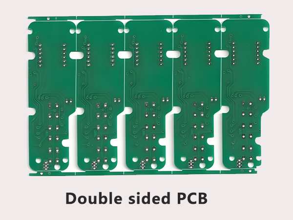
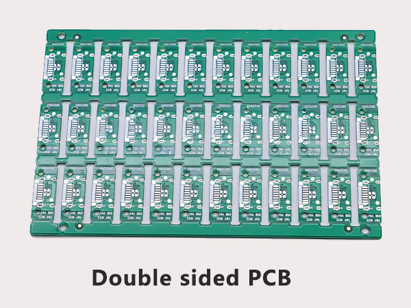
      A Double sided PCB is a printed circuit board with copper conductive layers on both the top and bottom surfaces, connected by plated through-holes (PTH) to enable electrical interconnection between layers. Unlike single-sided PCBs, double sided PCBs offer higher component density, more flexible routing options, and better signal integrity—making them ideal for mid-complexity electronic devices that require more functionality in a compact form factor.

      The core structure of a Double sided PCB includes a substrate (typically FR-4), copper layers on both sides, solder mask to protect the copper, and silkscreen for component labeling. This design balances cost-effectiveness and performance, making it one of the most widely used PCB types across industries.

      Double sided PCB Manufacturing Process: Step-by-Step Guide

      The Double sided PCB manufacturing process follows a precise sequence to ensure quality and consistency. Below is a detailed, easy-to-understand breakdown of each step:

      1. Substrate Preparation: Start with a high-quality substrate (most commonly FR-4), cut to the required size, and cleaned to remove dust, oil, and contaminants. This ensures strong adhesion of the copper layers to the substrate.
      2. Copper Lamination: The substrate is laminated with thin copper foil (typically 1oz, 35μm) on both sides using heat and pressure. This creates the conductive layers that form the Double sided PCB’s circuit paths.
      3. Circuit Patterning (Photolithography): A photoresist layer is applied to both copper surfaces, then exposed to UV light through a photomask (printed with the desired circuit pattern). The unexposed photoresist is removed, leaving the copper pattern that will become the circuit traces.
      4. Etching: The exposed copper (not protected by photoresist) is etched away using a chemical solution, leaving only the desired circuit traces on both sides of the Double sided PCB. The remaining photoresist is then stripped.
      5. Drilling: Holes (plated through-holes, PTH) are drilled through the PCB to connect the top and bottom copper layers. We use precision drilling equipment to ensure hole accuracy, with a minimum drill size of 0.3mm for standard applications.
      6. Plating: The drilled holes are metalized with copper (average thickness ≥20μm, minimum 18μm) to create electrical connections between the top and bottom layers. This step ensures reliable conductivity across the Double sided PCB.
      7. Solder Mask Application: A solder mask (usually green, but customizable) is applied to both sides of the PCB, covering all copper traces except for component pads, test points, and mark points. This protects the traces from oxidation and prevents short circuits during assembly.
      8. Silkscreen Printing: Component labels, part numbers, and polarity marks are printed on the solder mask using silkscreen. We follow standard specifications (30mil font height, 5mil font width) to ensure readability and avoid assembly errors.
      9. Final Inspection & Testing: The finished Double sided PCB undergoes rigorous inspection (visual and automated) to check for defects like short circuits, open circuits, or uneven solder mask. Electrical testing ensures all connections work as intended.

      Double sided PCB Design Guide: Solve Pain Points & Ensure Success

      Designing a Double sided PCB requires balancing component layout, routing, and manufacturability—common pain points that often lead to design errors, delayed production, or poor performance. Below, we break down the most critical design concerns and how EBest solves them for you.

      What Are the Most Common Double sided PCB Design Pain Points?

      • Wiring Congestion & Signal Crosstalk: With only two layers, routing complex signals (digital, analog, high-frequency) often leads to congestion and crosstalk, which degrades signal integrity.
      • Via Mismanagement: Poor via selection or placement introduces parasitic inductance and capacitance, causing signal distortion and reliability issues.
      • Component Interference: Placing components on both sides can lead to spatial interference, especially with tall components, affecting assembly and mechanical stability.
      • Manufacturability Issues: Designing features (e.g., overly narrow line widths, small holes) that exceed manufacturing capabilities leads to rework and delays.

      How EBest Solves Your Double sided PCB Design Challenges

      • Wiring & Crosstalk Solutions: Our engineers recommend a “layer partitioning” strategy—place digital signals and power on the top layer, and analog signals and ground on the bottom layer. We also enforce minimum line spacing (≥8mil) and isolate high-frequency signals (≤10cm in length) to reduce crosstalk to ≤-30dB.
      • Via Optimization: We guide you to select the right via type (standard 0.3-0.5mm for power/signals, microvias for high-frequency) and placement (≤2 vias per high-frequency path, ground vias within 0.3mm of signal vias) to minimize parasitic effects.
      • Component Layout Support: We provide 3D layout checks to avoid component interference, recommend keeping tall components on one side, and ensure ≥2mm spacing between functional areas.
      • Free DFM Analysis: Our team reviews your Double sided PCB design before production, identifying and fixing manufacturability issues (e.g., line width, hole size) to avoid rework and ensure a smooth production process.

      For hassle-free Double sided PCB design, trust EBest’s engineering team to guide you from concept to final design. We ensure your design is optimized for performance, manufacturability, and cost-efficiency—contact us today to get started.

      High-Quality Double sided PCB Prototype: Fast, Reliable & Customizable

      A high-quality Double sided PCB prototype is critical to validating your design, identifying issues early, and accelerating time-to-market. However, prototype projects often face common pain points that slow down development—here’s how EBest solves them.

      Common Double sided PCB Prototype Pain Points

      • Long Lead Times: Many manufacturers take weeks to deliver prototypes, delaying design validation and project timelines.
      • Poor Prototype Quality: Prototypes with inconsistent copper thickness, uneven solder mask, or faulty vias lead to inaccurate testing results.
      • Inflexible Customization: Difficulty adapting prototypes to design changes forces costly rework or redesigns.
      • Lack of Technical Support: Uncertainty about whether the prototype meets design requirements, with no guidance on testing or adjustments.

      EBest’s Double sided PCB Prototype Solutions

      • Fast Turnaround: We deliver high-quality Double sided PCB prototypes in days, not weeks, ensuring you can validate your design quickly and keep your project on track.
      • Premium Quality Prototypes: Our prototypes use the same high-quality materials and manufacturing processes as mass-produced Double sided PCBs, with strict quality checks to ensure accurate performance testing.
      • Flexible Customization: We support quick design changes and small-batch prototypes (flexible MOQ), allowing you to iterate on your design without costly delays.
      • End-to-End Support: Our engineers provide testing guidance, review prototype results, and help you refine your design to ensure the final Double sided PCB meets all your requirements.

      For fast, reliable, and customizable Double sided PCB prototypes, EBest is your trusted partner. We turn your design into a functional prototype quickly, helping you accelerate development and bring your product to market faster—contact us to request a prototype quote.

      How to Choose Double sided PCB Raw Materials? (Comparison Table)

      Choosing the right raw materials is critical to the performance, durability, and reliability of your Double sided PCB. Below is a detailed comparison of common materials, their properties, and ideal applications to help you make the right choice.

      Material TypeKey PropertiesTg ValueFlame RatingIdeal ApplicationsEBest Recommendation
      FR-4 (Epoxy Glass Cloth)Excellent mechanical strength, good electrical insulation, cost-effective, easy to process130°C – 180°C+UL94 V-0Consumer electronics, industrial control, communication devices, computersMost common choice for standard Double sided PCB projects
      High-Tg FR-4Higher heat resistance, better dimensional stability, improved reliability at high temperatures≥170°CUL94 V-0Automotive electronics, power electronics, high-temperature industrial applicationsFor projects exposed to high temperatures (≥150°C)
      PTFE (Polytetrafluoroethylene)Low dielectric loss, stable dielectric constant, excellent high-frequency performance260°C+UL94 V-0High-frequency communication devices, RF applications, aerospaceFor high-frequency (≥100MHz) Double sided PCB designs
      Aluminum SubstrateExcellent heat dissipation, good mechanical strength, electrical insulation130°C – 150°CUL94 V-0LED lighting, power electronics, automotive LED modulesFor heat-generating Double sided PCB applications

      Double sided PCB Applications: Industry Use Cases & Problem-Solving

      Double sided PCBs are widely used across industries due to their balance of performance, cost, and compact design. Below are four popular industries, real-world case studies, and common application challenges—with EBest’s solutions.

      1. Consumer Electronics

      Common applications: Smartphones, tablets, wearables, LED TVs, and home appliances. Double sided PCBs enable compact designs with high component density, critical for modern consumer devices.

      Case Study: We partnered with a consumer electronics brand to develop a Double sided PCB for a smartwatch. The challenge was fitting a battery management system, Bluetooth module, and sensors into a tiny form factor. Our solution: optimized component layout, 0.3mm vias, and a high-density routing strategy—resulting in a compact PCB that met all performance requirements and reduced assembly time by 20%.

      Common Problem & Solution: Signal interference between Bluetooth and power circuits. We separated digital and analog signals on different layers, added ground copper shielding, and reduced via count to minimize parasitic effects—eliminating interference completely.

      2. Automotive Electronics

      Common applications: Infotainment systems, sensors, engine control units (ECUs), and LED lighting. Double sided PCBs must withstand high temperatures, vibration, and harsh environments.

      Case Study: An automotive manufacturer needed a Double sided PCB for a dashboard infotainment system. The challenge was ensuring reliability in temperatures ranging from -40°C to 125°C. Our solution: high-Tg FR-4 material, thick copper traces (2oz), and reinforced vias—resulting in a PCB that passed all automotive environmental tests and had a 99.9% reliability rate.

      Common Problem & Solution: PCB warping due to temperature changes. We used high-Tg FR-4 and optimized copper distribution (grid patterns on large copper areas) to reduce thermal stress—preventing warping and ensuring long-term reliability.

      3. Industrial Control/Automation

      Common applications: PLCs (Programmable Logic Controllers), sensors, motor drives, and industrial monitors. Double sided PCBs must handle high voltages, noise, and continuous operation.

      Case Study: We worked with an industrial automation company to design a Double sided PCB for a motor drive controller. The challenge was isolating high-voltage (220V) and low-voltage (3.3V) circuits to avoid arcing. Our solution: 8mm spacing between high and low voltage areas, a blank isolation band, and grounded via arrays—ensuring safety and reducing noise by 35%.

      Common Problem & Solution: Electrical noise affecting sensor signals. We added decoupling capacitors, optimized ground paths, and used shielded traces—improving signal accuracy by 40%.

      4. Communication Devices

      Common applications: Routers, modems, Bluetooth devices, and IoT sensors. Double sided PCBs must support high-frequency signals with minimal loss.

      Case Study: A communication brand needed a Double sided PCB for a 5G router. The challenge was maintaining signal integrity for 5G frequencies (24-30GHz). Our solution: PTFE material, microvias (0.15mm), and controlled impedance routing—resulting in a PCB with signal loss ≤0.2dB per cm and meeting 5G performance standards.

      Common Problem & Solution: High-frequency signal attenuation. We used low-loss PTFE material and minimized via count (≤1 via per signal path)—reducing signal loss by 50%.

      What Are the Key Differences Between Double sided PCB and Single-Sided PCB?

      Many designers wonder whether to choose a Double sided PCB or single-sided PCB for their project. The answer depends on component density, signal complexity, and space requirements—here’s a clear comparison to help you decide.

      FeatureDouble sided PCBSingle-Sided PCB
      Copper Layers2 layers (top and bottom), connected by vias1 layer (only top or bottom)
      Component DensityHigh—components can be placed on both sidesLow—components only on one side
      Routing FlexibilityHigh—crossing traces can be routed via viasLow—traces cannot cross without rerouting
      Signal IntegrityBetter—supports high-frequency signals with less crosstalkPoor—limited to low-frequency, simple signals
      Ideal ApplicationsConsumer electronics, automotive, industrial control, communication devicesSimple devices (toys, remote controls, basic sensors)

      FAQ: Common Double sided PCB Questions & Solutions

      Below are the most frequently asked questions about Double sided PCBs, with clear, concise answers to help you solve common problems and make informed decisions.

      1. What is the minimum line width and spacing for a Double sided PCB?

      The minimum line width and spacing for a Double sided PCB is 6mil (0.15mm), but we recommend 8mil (0.2mm) for most projects. 6mil is possible but increases manufacturing complexity and lead time. For high-current applications, use wider lines (e.g., 1mm line width for 2A current with 1oz copper).

      2. How to prevent via failure in Double sided PCB?

      To prevent via failure, ensure via plating thickness is ≥20μm (average), use a pad diameter 2-2.5 times the via diameter, and avoid dense via placement (minimum 1mm center-to-center spacing). Also, reinforce vias near the PCB edge (≥1mm from the edge) to prevent cracking during cutting.

      3. Can Double sided PCB support high-frequency signals?

      Yes, Double sided PCBs can support high-frequency signals (up to 100MHz+) with the right design and materials. Use low-loss materials (e.g., PTFE), minimize via count, keep high-frequency traces short (≤10cm), and add ground vias near signal vias to reduce parasitic effects.

      4. What is the maximum temperature a Double sided PCB can withstand?

      The maximum temperature depends on the substrate material: standard FR-4 Double sided PCBs can withstand continuous temperatures up to 130°C, high-Tg FR-4 up to 180°C, and PTFE up to 260°C. For automotive or high-temperature applications, choose high-Tg FR-4 or PTFE.

      5. How to reduce crosstalk in Double sided PCB design?

      Reduce crosstalk by separating digital and analog signals on different layers, maintaining minimum line spacing (≥1.5x line width), keeping high-frequency traces short, and adding ground copper shielding around sensitive signals. Also, avoid parallel routing of high-frequency traces for long distances.

      6. What is the difference between plated through-holes (PTH) and non-plated through-holes (NPTH) in Double sided PCB?

      PTHs are metalized (copper-plated) to connect the top and bottom copper layers electrically, used for component pins and signal interconnection. NPTHs are non-metalized, used for mechanical mounting (e.g., screws) and do not conduct electricity. We default to PTHs unless specified otherwise.

      7. How long does it take to manufacture a Double sided PCB prototype?

      At EBest, Double sided PCB prototypes are delivered in 2-5 business days, depending on complexity. Mass production lead times vary based on order quantity but typically range from 7-14 business days—we prioritize fast delivery without compromising quality.

      Choose EBest for Your Double sided PCB Needs

      We provide high-quality Double sided PCB design, prototype, and manufacturing services, tailored to meet the unique needs of your project. Whether you need a custom Double sided PCB for consumer electronics, automotive, industrial control, or communication devices, our team of engineers is here to guide you every step of the way. For reliable, fast, and cost-effective Double sided PCB solutions, contact us to place your order at sales@bestpcbs.com. EBest—your trusted partner for all Double sided PCB needs.

      You may also like

      High Quality PCB Prototype Services in Israel | Free DFM with Custom Solutions

      March 9th, 2026

      PCB prototype services in Israel are critical for turning design concepts into functional products, and EBest delivers reliable, high-standard solutions tailored to local needs. We focus on solving common pain points in local prototyping, ensuring each PCB prototype services in Israel meets strict quality and delivery requirements, backed by decades of industry experience and advanced manufacturing capabilities.

      High Quality PCB Prototype Services in Israel, https://www.bestpcbs.com/blog/2026/03/pcb-prototype-services-in-israel/

      Are You Facing these Challenges of PCB Prototype Services in Israel?

      • Can local PCB prototype services in Israel meet tight delivery deadlines for urgent projects?
      • Do local prototyping providers offer free DFM analysis to avoid design errors?
      • Can local prototype services support small-batch custom orders with low MOQ?
      • Are local prototyping providers certified to meet medical and aerospace industry standards?
      • Can PCB prototype services in Israel ensure consistent quality across multiple prototype runs?
      • Do local prototype services provide full production data traceability?
      • Can local prototype services handle specialized board types like ceramic or flexible PCBs?

      One-Stop Solutions for PCB Prototyping in Israel

      • Urgent Delivery Solution: We offer 24-hour expedited PCB prototype services in Israel, with automated production equipment including LDI laser imaging to reduce pre-production time, ensuring urgent orders ship within one day without compromising quality.
      • Free DFM Analysis Solution: Our professional team provides free DFM analysis for all PCB prototyping in Israel orders, checking soldering pad design, component layout, and process compatibility to eliminate design errors before production, reducing rework and delays.
      • Small-Batch Custom Solution: We support low MOQ for PCB prototype in Israel orders, with flexible manufacturing modules that quickly switch between different board specifications, making small-batch custom prototyping cost-effective and efficient.
      • Certified Quality Solution: Our PCB prototyping service in Israel meets strict industry certifications, including ISO 13485 for medical and AS9100D for aerospace, ensuring prototypes comply with local and international standards.
      • Consistent Quality & Traceability Solution: We use an MES system to track all production data for PCB prototype services in Israel, from raw material inspection to final testing, ensuring consistent quality and full traceability for every prototype.
      • Specialized Board Solution: We offer a full range of specialized PCB prototyping in Israel services, including ceramic, flexible, and metal-based PCBs, with advanced manufacturing techniques to handle complex board requirements.

      Why Choose EBest for PCB Prototype Services in Israel?

      Since 2006, EBest has built 19+ years of trusted expertise in PCB manufacturing. You can skip the guesswork and partner with a provider that truly understands your prototyping goals, including delivering reliable PCB prototype services in Israel. We invest heavily in R&D to stay ahead of industry innovations, ensuring you always have access to the latest manufacturing techniques. Our 260,000 square feet monthly production capacity and ability to complete 1,000+ unique board types mean we never turn down your complex or specialized prototyping needs. This eliminates the hassle of working with multiple providers, saving you valuable time and streamlining your entire prototyping process.

      We design our services entirely around your priorities: speed to market, flexibility, and cost savings. Our 24-hour quick-turn prototyping slashes your project timelines to help you launch faster than competitors and secure your market advantage. We remove high MOQ barriers with a starting order quantity of just 1 unit. This lets you test design concepts affordably without wasting budget on unnecessary volume, keeping your development costs low while maintaining flexibility. Our free DFM analysis eliminates costly design errors and rework to protect your budget and keep your projects on track. We use only premium materials and enforce strict quality control to ensure your prototypes perform reliably, even for the most demanding applications.

      Your peace of mind is our top priority. Our services are backed by industry-leading certifications including ISO 9001:2015, ISO 13485:2016, and AS9100D. These certifications guarantee compliance with medical, aerospace, and general manufacturing standards so you never face costly compliance delays or rejections. Our real-time MES production tracking gives you full transparency into every step of your order. You can monitor progress anytime to stay informed and in control. Our personalized support team is always available to address your unique needs, ensuring a seamless and stress-free experience from quote to delivery.
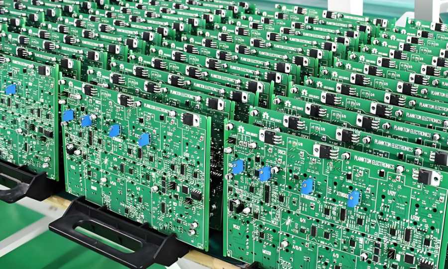
      Why Choose EBest for PCB Prototype Services in Israel, https://www.bestpcbs.com/blog/2026/03/pcb-prototype-services-in-israel/

      What Quality Certifications Do We Have for PCB Prototyping in Israel?

      Below are quality certifications we have for PCB prototyping in Israel:

      • ISO 9001:2015: Ensures our PCB prototype services in Israel follow strict quality management systems, guaranteeing consistent product quality and customer satisfaction.
      • ISO 13485:2016: Certified for medical device PCB prototyping, meeting the strict safety and quality requirements for medical applications, including biocompatibility and risk management standards.
      • AS9100D: Certified for aerospace PCB prototyping, complying with the rigorous quality standards for aerospace and defense applications.
      • IATF 16949: Certified for automotive PCB prototyping, ensuring prototypes meet automotive industry quality and reliability requirements.
      • UL: Ensures our PCB prototypes meet safety standards for electrical components, suitable for global markets including Israel.
      • REACH & RoHS: Compliant with environmental standards, ensuring our PCB prototyping in Israel is free from harmful substances.

      How We Ensure On-Time Delivery of Israel PCB Prototype Orders?

      Here are our methods for ensuring on-time delivery of PCB prototype orders from Israel:

      • Automated Production Equipment: We use advanced automated LDI laser imaging, automated dry film presses, and quick-change production modules. These tools cut down production time significantly, ensuring efficient processing of your prototypes and eliminating unnecessary delays in drilling, etching, and other key steps.
      • Real-Time MES System Scheduling: Our MES (Manufacturing Execution System) tracks your order progress in real time. It optimizes production resource allocation to avoid bottlenecks and sends instant alerts to our team if potential delays arise. This proactive approach lets us make timely adjustments and keep your order on track.
      • Dedicated Project Teams: Every order is assigned a dedicated project team responsible for design review, production oversight, and testing. This ensures clear communication, fast problem-solving, and no missteps, so your prototype moves smoothly from start to finish without unnecessary hold-ups.
      • Strategic Material Stocking: We maintain a steady stock of common PCB materials, including FR4, ceramic, and metal cores. This eliminates material shortages that often cause delays, allowing production to start immediately once your design is approved.
      • Streamlined Quality Control: Our pre-production and in-production quality checks are designed to catch issues early. By identifying and resolving defects before they escalate, we reduce rework and ensure your prototype is completed on schedule, with no costly delays from fixes later in the process.
      How We Ensure On-Time Delivery of Israel PCB Prototype Orders? https://www.bestpcbs.com/blog/2026/03/pcb-prototype-services-in-israel/

      Our Lead Time for Israel PCB Prototyping Orders

      TypeLead Time (Standard)Lead Time (Expedited)
      Single-Sided FR4 PCB Prototype2-3 business days24 hours
      Multi-Layer (2-8 Layers) PCB Prototype3-5 business days48 hours
      Flexible/Rigid-Flex PCB Prototype5-7 business days72 hours
      Ceramic/Metal Core PCB Prototype7-10 business days5 business days
      High-Frequency/RF PCB Prototype6-8 business days4 business days

      Our Quality Inspection Processes for Israel PCB Prototyping Orders

      Below are quality inspection processes for Israel PCB prototyping orders:

      • Raw Material Inspection: All materials for PCB prototype services in Israel are inspected for quality and compliance with standards, including material composition and thermal stability, with test records stored in the MES system.
      • Pre-Production Design Review: Our team conducts a detailed review of design files, including DFM analysis, to identify potential issues before production starts, ensuring design compatibility with manufacturing processes.
      • In-Production Inspection: Key production steps (drilling, etching, soldering) are inspected in real time, using automated AOI and X-Ray equipment to detect defects such as short circuits, open circuits, and poor soldering.
      • Electrical Performance Testing: Each prototype undergoes electrical testing, including continuity, impedance, and voltage resistance tests, to ensure it meets design specifications.
      • Final Visual Inspection: Finished prototypes are visually inspected for surface defects, dimensional accuracy, and overall quality, with only passing units approved for delivery.
      • Post-Delivery Quality Follow-Up: We follow up with clients to confirm prototype performance, addressing any issues promptly and continuously improving our PCB prototyping in Israel processes.
      Our Quality Inspection Processes for Israel PCB Prototyping Orders, https://www.bestpcbs.com/blog/2026/03/pcb-prototype-services-in-israel/

      Case Studies of Medical Israel PCB Prototype Services

      Project Background:

      An Israeli medical device company sought a high-precision ceramic PCB prototype for its portable diagnostic device. The project required strict compliance with ISO 13485 standards, it is critical for medical equipment and rigorous biocompatibility requirements, as the prototype would integrate with patient-facing diagnostic tools.

      Project Requirements:

      The client specified a 4-layer ceramic PCB with high thermal conductivity to support the device’s heat management needs. Key requirements included 50Ω impedance control, a compact 50mm×30mm design, and 20 total prototypes. The team needed delivery within 7 days, with all units meeting strict medical device safety standards.

      Project Challenges:

      Ceramic PCB manufacturing demands precise temperature control during firing to prevent cracking, a common pain point with this material. The tight ±5% impedance tolerance added complexity, requiring exact trace design. The 7-day lead time left no room for rework, and the prototype also needed to pass ISO 10993 biocompatibility testing to ensure safety for medical use.

      Our Solutions:

      To address these challenges, we used high-purity ceramic materials and optimized our firing process with temperature stabilization technology to eliminate cracking. Our engineering team adjusted trace layouts and used advanced impedance simulation software to meet the 50Ω requirement consistently. We prioritized the order in our production schedule, assigning a dedicated team and using expedited processes to ensure on-time delivery. We also conducted pre-delivery ISO 10993 biocompatibility testing to confirm compliance before shipping.

      Output Results:

      We delivered all 20 prototypes in 6 days, one day ahead of the client’s 7-day deadline. The project achieved a 99.8% yield, with every unit passing impedance and biocompatibility tests. The client reported zero defects during device testing and field trials, with the prototypes performing flawlessly in their portable diagnostic tool. Impressed by our reliability and quality, the client now partners with EBest for all their PCB prototype services in Israel.

      FAQs of PCB Prototyping Services in Israel

      Q1: Can I get PCB prototype services in Israel with a lead time shorter than 24 hours?
      A1: Yes, for simple single-sided FR4 prototypes with urgent needs, we can achieve 12-hour expedited delivery. We prioritize urgent orders and use automated production equipment to minimize processing time, ensuring fast delivery without compromising quality.

      Q2: Do you provide free DFM analysis for PCB prototyping in Israel?
      A2: Yes, we offer free DFM analysis for all PCB prototype in Israel orders. Our team reviews design files to identify potential manufacturing issues, such as incorrect soldering pads size, insufficient spacing, or incompatible materials, helping you avoid rework and delays.

      Q3: What is the minimum order quantity for PCB prototyping service in Israel?
      A3: Our MOQ for PCB prototype services in Israel is 1 unit. We support small-batch custom orders, making it easy for clients to test design concepts without large upfront costs. We also offer volume discounts for larger prototype orders.

      Q4: Are your PCB prototype services in Israel compliant with Israeli ICT safety standards?
      A4: Yes, all our PCB prototypes comply with the latest Israeli SI 62368 standard for ICT equipment safety, as well as international standards. Our certifications (ISO 9001, ISO 13485, AS9100D) ensure compliance with local and global requirements.

      Q5: Can you track the production progress of my PCB prototype in Israel order?
      A5: Yes, we use an MES system to track production data in real time. You can request updates on your PCB prototyping in Israel order at any time, including material inspection, production status, and testing results, ensuring full transparency.

      Choose EBest for PCB Prototype Services in Israel

      Choose EBest for PCB prototype services in Israel, your trusted partner for high-quality, reliable prototyping that moves your projects forward. We don’t just deliver prototypes; we deliver peace of mind with free DFM analysis to avoid costly rework, 24-hour expedited delivery to keep you ahead of deadlines, low MOQ (starting at 1 unit) to fit your budget, and full compliance with industry certifications (ISO 9001, ISO 13485, AS9100D) to guarantee safety and reliability.

      Whether you’re building medical devices, aerospace components, or industrial equipment, our 19+ years of expertise and proven track record with Israeli clients mean we have the experience and capabilities to bring your designs to life. Stop settling for delays, inconsistencies, or one-size-fits-all solutions. Contact us today at sales@bestpcbs.com to place your order and experience the EBest difference, where your success is our priority.

      You may also like

      PCB Via Types: What Are the Different Types of Vias in PCB?

      March 6th, 2026

      As electronic products become smaller and more complex, engineers rely on different types of vias in PCB layouts to achieve dense routing, high-speed signal integrity, and thermal stability. Without vias, multilayer PCB architecture would not function efficiently. Each via structure serves a specific purpose. Some focus on basic connectivity, others support HDI routing, RF performance, or thermal transfer.

      A typical multilayer PCB may contain hundreds or even thousands of vias depending on circuit density. According to common PCB fabrication guidelines, the most frequently used via diameter ranges between 0.2 mm and 0.5 mm, while high-density designs may use microvias smaller than 0.15 mm.

      In this guide, we explain the most widely used PCB via types, how they work, and when engineers should apply them. The article also compares via filling technologies and explains the difference between vias and PTH holes.

      PCB Via Types: What Are the Different Types of Vias in PCB?

      1. Through-Hole Vias

      Through-hole vias are the most traditional and widely used PCB via types. They pass completely through the entire PCB stack, connecting the top layer to the bottom layer. In standard PCB manufacturing, mechanical drilling machines can achieve drill diameters from 0.15 mm to 6 mm. For most multilayer boards, the common finished via hole size ranges from 0.2 mm to 0.4 mm.

      Another important parameter is the aspect ratio, which describes the ratio of board thickness to via hole diameter. Most PCB manufacturers recommend keeping the aspect ratio within 6:1 to 10:1 to ensure stable plating quality.

      1. Through-Hole Vias

      Typical characteristics of through-hole vias:

      • Connect all PCB layers
      • Larger drill diameters compared with HDI vias
      • Lower fabrication cost
      • Suitable for conventional multilayer PCB designs
      • Reliable mechanical strength

      However, through-hole vias occupy routing space on every layer they pass through. This can reduce layout flexibility when board density increases.

      Typical applications include:

      • Power distribution networks
      • Ground connections
      • Standard digital circuits
      • Industrial electronics

      Despite newer HDI technologies, through-hole vias remain an essential structure in many PCB designs.

      2. Blind Vias

      Blind vias connect the outer layer of a PCB to one or more inner layers, but they do not extend through the entire board.

      For example, a blind via may connect the top layer to layer two or layer three, while leaving the remaining layers untouched. This design helps engineers save routing space on deeper layers.

      Typical blind via depths are usually less than 0.3 mm, depending on the PCB stack-up structure. Laser-drilled blind vias often have diameters between 0.075 mm and 0.15 mm.

      Blind Vias

      Advantages of blind vias include:

      • Improved routing density
      • More available space on internal layers
      • Better signal routing for compact boards
      • Reduced interference between layers

      Blind vias are widely used in high-density electronics where layout space is limited.

      Common applications include:

      • Smartphones
      • IoT devices
      • compact industrial controllers
      • RF modules

      Blind vias help designers maintain a clean routing structure without drilling through the entire PCB stack.

      3. Buried Vias

      Buried vias connect inner PCB layers but do not reach the outer layers. They remain completely hidden within the board structure after lamination.

      These vias are created during intermediate lamination stages. Manufacturers first drill and plate the internal layers, then laminate additional layers on top.

      Typical buried via diameters are similar to standard mechanical vias, usually ranging from 0.2 mm to 0.3 mm.

      Benefits of buried vias include:

      • Increased routing density
      • Cleaner surface layout
      • Reduced via congestion
      • Better signal performance in complex designs

      However, buried vias increase fabrication complexity. They also require multiple lamination cycles.

      For example, a PCB with buried vias and blind vias may require 2–3 lamination cycles, increasing production cost.

      Typical uses include:

      • HDI PCB designs
      • advanced communication equipment
      • networking hardware
      • high-performance computing systems

      Buried vias are especially useful when engineers must route many signals across multiple layers.

      4. Stacked Vias

      Stacked vias are a vertical arrangement of microvias placed directly on top of each other. Each microvia connects two adjacent layers, this structure creates a continuous vertical connection through several layers.

      Stacked vias are commonly used in HDI PCB designs. They support extremely high routing density and are often placed under fine-pitch components such as BGA packages. Fine-pitch BGA packages often have ball pitches of 0.5 mm or smaller, making stacked microvias necessary for signal escape routing.

      Stacked Vias

      Key characteristics of stacked vias:

      • Vertical alignment of multiple microvias
      • Supports high-density routing
      • Suitable for fine-pitch BGA packages
      • Requires via filling and copper plating

      Because stacked vias require precise alignment and filling processes, manufacturing cost is higher.

      However, the structure provides excellent electrical performance and compact routing paths.

      5. Staggered Vias

      Staggered vias are an alternative to stacked vias. Instead of aligning microvias vertically, each via is slightly offset from the one above or below.

      Staggered Vias

      Advantages of staggered vias include:

      • Improved mechanical reliability
      • Lower fabrication difficulty
      • Reduced risk of via cracking
      • Suitable for HDI structures

      Engineers often choose staggered vias when cost control is important but high routing density is still required.

      These vias are frequently used in:

      • consumer electronics
      • automotive control boards
      • communication equipment

      Staggered vias provide a balanced solution between performance and manufacturing complexity.

      6. Microvias

      Microvias are very small vias typically created by laser drilling. They are an essential element of HDI PCB technology. Microvias usually connect only two adjacent layers, so their diameter is significantly smaller than traditional vias. Typical microvia diameter ranges between 50 μm and 150 μm.

      Because of their small size, microvias allow designers to route signals between fine-pitch component pads.

      Microvias

      Key advantages of microvias:

      • Extremely high routing density
      • Shorter signal paths
      • Lower parasitic inductance
      • Improved signal integrity

      Microvias are commonly used in advanced electronics such as:

      • smartphones
      • wearable devices
      • aerospace systems
      • high-speed communication equipment

      Although microvias improve performance, they require specialized fabrication equipment and strict process control.

      7. Vias in Pad

      Vias in pad refer to vias placed directly inside the component pad area. This design is common in fine-pitch packages such as BGA or QFN devices. The via allows signals to transition immediately from the pad to inner routing layers.

      However, vias in pad require filling and planarization before component assembly. Without proper filling, solder can flow into the via hole during reflow.

      Vias in Pad

      Advantages of vias in pad include:

      • Reduced signal path length
      • Improved routing density
      • Better thermal transfer
      • Ideal for fine-pitch BGA packages

      8. Vias on Pad

      Vias on pad are slightly different from vias in pad. In this structure, the via is placed very close to the pad rather than directly inside it.

      The via may partially overlap with the pad area depending on design requirements. This method helps engineers maintain efficient routing while reducing the risk of solder wicking.

      Key features of vias on pad include:

      • Easier manufacturing compared with via-in-pad
      • Lower cost than filled vias
      • Suitable for many standard BGA layouts
      • Good compromise between density and reliability

      Designers often use this structure when full via-in-pad technology is not required.

      What Is the Difference Between Via and PTH in PCB?

      Many engineers confuse vias with plated through holes (PTH). Although they share a similar manufacturing process, their functions differ.

      The following table explains the main differences.

      FeatureViaPTH (Plated Through Hole)
      Main functionElectrical interconnection between layersMounting hole for components
      Diameter0.1–0.5 mm typical0.6–1.2 mm typical
      Component insertionNot intended for component leadsDesigned for component leads
      Assembly processNo component insertionUsed in through-hole assembly
      Common useSignal routing and power connectionsMechanical support and electrical connection

      In simple terms, a via connects PCB layers, while a PTH hole supports component leads while also providing electrical connectivity.

      Via Filling Types in PCB

      In advanced PCB manufacturing, vias are often filled to improve reliability and assembly quality. Several via filling methods are commonly used, including:

      1. Conductive Paste Fill

      Conductive paste fill involves filling the via with a conductive material such as silver epoxy.

      Advantages:

      • Good electrical conductivity
      • Relatively simple process
      • Suitable for certain thermal applications

      However, paste materials may not provide the same mechanical strength as copper filling.

      2. Resin Plugging

      Resin plugging uses epoxy resin to fill the via hole. After filling, the surface is planarized to create a flat pad.

      Key benefits include:

      • Prevents solder wicking
      • Improves assembly reliability
      • Suitable for via-in-pad structures

      Resin plugging is widely used in HDI PCBs and BGA assemblies.

      3. Copper Fill (Via Plating)

      Copper filling is the most advanced via filling method. The via hole is completely filled with electroplated copper.

      Advantages include:

      • Excellent thermal conductivity
      • Strong mechanical stability
      • High electrical reliability
      • Ideal for stacked microvias

      Copper-filled vias are common in high-performance PCBs used in aerospace, telecommunications, and advanced computing systems.

      EBest Circuit: One-Stop PCB Manufacturer with Any PCB Via Types

      At EBest Circuit (Best Technology), we support a wide range of PCB via structures for both standard multilayer boards and advanced HDI designs. Our engineering team works closely with customers during the early design stage to review via structures, optimize manufacturability, and improve long-term reliability.

      Our capabilities include:

      • Mechanical drilling down to 0.15 mm
      • Laser microvia drilling to 75 μm
      • HDI stack-up structures such as 1+N+1, 2+N+2, 3+N+3, 4+N+4
      • Copper-filled stacked microvias
      • Blind and buried via fabrication
      • Professional DFM review before production
      • Guidance on selecting the right PCB via types
      • Optimization for HDI stack-up structures
      • Manufacturing support for microvias, blind vias, and buried vias
      • Full PCB fabrication and PCBA assembly service

      If you are designing a multilayer PCB or HDI board and need professional manufacturing support, working with an experienced PCB partner can simplify the entire development process.

      For project consultation, DFM review, or PCB manufacturing services, feel free to contact EBest Circuit (Best Technology) at: sales@bestpcbs.com. Our engineering team is always ready to help bring your PCB designs into reliable production.

      You may also like

      What is Empty Circuit Board? Empty Circuit Board vs Assembled PCB

      March 5th, 2026

      An empty circuit board is the starting point of almost every electronic product. Before chips, resistors, and connectors appear on a board, engineers begin with a bare platform that carries electrical pathways and mechanical structure. This base platform is the empty circuit board, also called a bare PCB.

      EBest Circuit (Best Technology) has more than 19 years of PCB fabrication and assembly experience. Our engineering team supports projects from design review to final assembly. With integrated PCB fabrication and PCBA production, customers receive consistent quality, fast delivery, and practical engineering support throughout the process.

      What Is an Empty Circuit Board?

      An empty circuit board refers to a printed circuit board before electronic components are mounted. It contains copper traces, vias, pads, and insulating substrate materials. These elements form the electrical network that later connects components.

      In manufacturing terms, an empty circuit board is often called:

      • Bare PCB
      • Blank PCB
      • Fabricated PCB

      The board becomes a finished electronic module only after component assembly. That stage is known as PCBA (Printed Circuit Board Assembly).

      What Materials Are Used in an Empty Circuit Board?

      The materials inside an empty circuit board determine electrical performance and durability. Most boards combine insulating substrate materials with conductive copper layers.

      1. Substrate Materials

      The substrate forms the structural foundation of the PCB. Common substrate materials include:

      • FR4 fiberglass epoxy – the most widely used PCB material
      • High-TG FR4 – suitable for higher thermal environments
      • Polyimide – used for flexible circuits
      • Aluminum core – used for heat dissipation
      • Ceramic materials – used in high-frequency electronics

      Among these options, FR4 remains the standard choice because it balances cost, strength, and electrical insulation.

      2. Copper Layers

      Copper forms the conductive pathways on the board. These traces connect electronic components. Copper thickness is measured in ounces (OZ) per square foot. Typical copper thickness values include:

      Copper WeightThicknessApplication
      0.5 oz~17 µmFine-line circuits
      1 oz~35 µmStandard electronics
      2 oz~70 µmPower electronics
      3 oz+100 µm+High-current circuits

      Higher copper thickness improves current capacity and thermal performance.

      3. Solder Mask

      Solder mask is the colored protective layer on top of the PCB. It prevents solder bridging during assembly. Common colors include:

      • Green
      • Black
      • Blue
      • White
      • Red

      Green remains the most common color because it offers good contrast for inspection.

      4. Surface Finish

      The copper pads require protective coating. Surface finishes prevent oxidation and improve solderability. Typical finishes include:

      • HASL (Hot Air Solder Leveling)
      • ENIG (Electroless Nickel Immersion Gold)
      • ENEPIG
      • Immersion silver
      • OSP coating

      Each finish has advantages depending on product requirements.

      How Is an Empty Circuit Board Manufactured?

      Manufacturing an empty circuit board involves multiple precision processes. Each step builds part of the board structure. Below is a simplified overview of the process.

      1. Design File Preparation

      Engineers prepare design files using PCB design software. These files define trace routing, drill holes, and board dimensions. Typical design files include:

      • Gerber files
      • Drill files
      • Stack-up specifications

      2. Material Preparation

      3. Inner Layer Imaging

      4. Etching

      5. Lamination

      6. Drilling

      7. Copper Plating

      8. Solder Mask Application

      9. Surface Finish

      10. Electrical Testing

      If you want to know more the manufacturing process of empty circuit board, you can watch below video from our PCB fabrication workshop:

      What Are the Different Types of Empty Circuit Boards?

      Empty circuit boards are not all built the same. Engineers select different PCB structures based on circuit complexity, signal speed, thermal conditions, and mechanical requirements. Below are the most common types of empty circuit boards used in modern electronics manufacturing.

      1. Single-Layer Empty Circuit Board

        A single-layer circuit board contains one conductive copper layer on one side of the substrate. All components and traces appear on the same surface.

        Typical applications include:

        • LED lighting modules
        • Power adapters
        • Small household electronics
        • Simple control boards

        However, routing space is limited because all connections must exist on one layer.

        2. Double-Layer Empty Circuit Board

        A double-layer circuit board contains copper layers on both the top and bottom surfaces of the substrate. Electrical connections between the two layers are created using plated through holes (vias).

        Double-layer PCBs are widely used in:

        • consumer electronics
        • industrial control systems
        • communication devices
        • embedded modules

        Because they provide more routing space than single-layer boards, they remain a practical solution for medium-complexity designs.

        3. Multilayer Empty Circuit Board

        A multilayer PCB contains three or more copper layers stacked together through lamination. Some advanced boards may include 8, 12, or even more layers.

        Common applications include:

        • smartphones and tablets
        • computer motherboards
        • networking equipment
        • high-speed communication systems

        Although multilayer PCBs require more manufacturing steps, they enable compact designs and higher performance.

        4. Flexible Circuit Boards

        A flexible PCB uses polyimide or similar flexible substrate materials instead of rigid fiberglass. The board can bend, twist, or fold without damaging the circuit. Flexible boards reduce connector usage and improve space utilization in compact devices.

        Typical applications include:

        • wearable electronics
        • camera modules
        • medical instruments
        • portable consumer devices

        5. Rigid-Flex Circuit Boards

        A rigid-flex PCB combines rigid circuit board sections with flexible interconnections in a single structure.

        Rigid-flex boards are often used in:

        • aerospace electronics
        • medical equipment
        • military systems
        • advanced communication devices

        Although the design and manufacturing process are more complex, rigid-flex PCBs offer excellent durability and compact integration.

        Rigid-Flex Circuit Boards

        6. Metal Core Circuit Boards

        A metal core PCB (MCPCB) uses a metal base layer, usually aluminum or copper, instead of standard fiberglass. Metal core boards are widely used in:

        • high-power LED lighting
        • automotive lighting systems
        • power converters
        • industrial power modules

        Because thermal performance is critical in these applications, metal core boards provide a reliable solution.

        Metal Core Circuit Boards

        7. Ceramic Circuit Board

        A ceramic PCB uses ceramic materials such as aluminum oxide (Al₂O₃) or aluminum nitride (AlN) as the substrate instead of fiberglass. Ceramic materials provide excellent thermal conductivity, electrical insulation, and dimensional stability.

        Key advantages include:

        • excellent heat dissipation
        • high electrical insulation strength
        • stable performance at high temperatures
        • low signal loss at high frequencies

        Ceramic PCBs are widely used in:

        • RF communication modules
        • power semiconductor modules
        • laser equipment
        • automotive electronics
        • aerospace electronics

        Although ceramic boards are more expensive than standard FR4 PCBs, they deliver superior performance in demanding environments.

        Ceramic Circuit Board

        Where Are Empty Circuit Boards Used?

        Empty circuit boards serve as the base platform for almost all electronic products. Before components are mounted, the board provides routing paths, grounding structures, and mechanical support for the final system.

        Common applications include:

        • Consumer electronics – smartphones, smart home devices, wireless earbuds, and wearable gadgets
        • Computer hardware – motherboards, graphics cards, memory modules, and storage controllers
        • Automotive – engine control units, battery management systems, infotainment modules, and sensor interfaces
        • Industrial automation systems – PLC controllers, motor drivers, robotics control boards, and industrial power supplies
        • Communication equipment – routers, base stations, RF communication modules, and network switches
        • Medical devices – patient monitoring systems, diagnostic equipment, imaging systems, and portable healthcare electronics
        • LED lighting systems – commercial lighting, automotive lighting, and architectural illumination.

        How Much Does an Empty Circuit Board Cost?

        The cost of an empty circuit board varies widely. Several factors influence manufacturing price, major cost factors including:

        1. Board size

        2. Layer count

        3. Material type

        4. Copper thickness

        5. Surface treatment

        6. Production quantity

        Here is a general cost for empty circuit boards:

        PCB TypeTypical Cost Range
        Single layer$1 – $5
        Double layer$3 – $15
        Multilayer PCB$20 – $200+

        These values vary depending on complexity and quantity. Working with an experienced manufacturer helps control cost while maintaining quality.

        Empty Circuit Board vs Assembled PCB

        An empty circuit board and an assembled PCB represent two different stages in electronic manufacturing. The empty board provides the physical and electrical platform. The assembled PCB transforms that platform into a working electronic module. Below is comparison chart between them:

        ItemEmpty Circuit Board (Bare PCB)Assembled PCB (PCBA)
        DefinitionPCB structure without electronic componentsPCB with components soldered and fully functional
        Manufacturing StagePCB fabricationPCB assembly
        Main ProcessesLamination, drilling, plating, etching, solder mask, surface finishSMT placement, reflow soldering, wave soldering, inspection
        Electrical FunctionProvides conductive pathways but no active functionalityFully operational circuit
        Components InstalledNoneResistors, capacitors, ICs, connectors, sensors
        Typical Layer Count1–20+ layers depending on designSame as PCB but populated with parts
        Manufacturing TimeUsually 3–7 days for prototypes5–10 days depending on component sourcing
        Testing MethodElectrical continuity testFunctional test, AOI, X-ray inspection
        Cost StructureMostly determined by material, layer count, board sizeIncludes PCB cost, components, assembly labor
        WeightVery light since no components are installedHeavier due to electronic parts
        Application StageUsed during early design, testing, and prototypingUsed in final electronic products
        Production ComplexityMedium complexity fabricationHigher complexity due to placement accuracy
        Typical UseEngineering validation and prototypingConsumer electronics, industrial equipment, automotive electronics

        From a manufacturing perspective, the empty circuit board acts as the foundation of the electronic system. Once components are installed through SMT or THT assembly processes, the board becomes a functional PCBA ready for integration into a product.

        Why Choose EBest as Your Empty Circuit Board & Assembled PCB Manufacturer?

        Best Technology (EBest Circuit) is a PCB and PCBA manufacturer with 19 years of industry experience, headquartered in Shenzhen, one of the world’s most important electronics manufacturing hubs. To better support global customers and ensure flexible supply chains, we have established production facilities in both China and Vietnam, allowing us to provide stable manufacturing capacity and competitive lead times.

        Our advantages include:

        • 19 Years of PCB & PCBA Manufacturing Experience
        • Professional R&D and engineering team
        • 1+3 engineering support model
        • One-stop PCB Fabrication and PCBA Assembly
        • Rapid prototype and production turnaround
        • Full Digital Manufacturing System
        • No MOQ, flexible order quantities
        • Global customer support experience across North America, Europe, and Asia
        • ISO 9001, ISO 13485, IATF 16949, and AS9100D certificated

        If you are planning a new electronics project or looking for a dependable PCB manufacturing partner, feel free to contact our engineering team.

        📩 sales@bestpcbs.com

        We are always ready to support your next circuit board project.

        FAQs

        1. Is an empty circuit board the same as a PCB?

        Yes. An empty circuit board is commonly called a bare PCB. It includes copper traces and pads but no electronic components.

        2. What thickness do empty PCBs usually have?

        Typical PCB thickness ranges from 0.8 mm to 1.6 mm. Thinner boards exist for compact electronics, while thicker boards provide higher mechanical strength.

        3. What files are required to manufacture a PCB?

        Manufacturers usually require the following files:

        • Gerber files
        • Drill files
        • PCB stack-up information
        • Bill of materials (for assembly)

        These files define the complete board structure.

        You may also like

        PCB Thermal Conductivity Guide: Materials, Heat Dissipation & Thermal Design

        March 5th, 2026

        If you work with electronic devices, you’ve probably heard of PCB thermal conductivity. But do you know what it really means? Or why it matters for your projects? This guide breaks down everything you need to know—from key materials to design tips

        What Is PCB Thermal Conductivity?

        PCB thermal conductivity refers to the ability of a printed circuit board material to transfer heat from one location to another. It is typically measured in W/m·K (Watts per meter-Kelvin).

        A higher thermal conductivity value means heat travels more efficiently through the board. This helps prevent local hot spots and keeps electronic components operating within safe temperature limits.

        Electronic components generate heat during operation. If the PCB cannot dissipate this heat effectively, several problems may occur:

        • Component overheating
        • Reduced electrical performance
        • Accelerated material aging
        • Solder joint fatigue
        • Unexpected system failure

        Because of these risks, thermal performance is now a critical parameter in PCB design.

        What Is PCB Thermal Conductivity?

        What Is PCB Thermal Conductivity?

        Why Thermal Conductivity is Important in PCB?

        Thermal conductivity becomes especially important in systems such as:

        • LED lighting modules
        • automotive power electronics
        • RF communication equipment
        • industrial motor controllers
        • high-density computing hardware

        In these systems, components like MOSFETs, power regulators, and RF amplifiers can generate significant heat during operation. A properly designed PCB spreads that heat efficiently across copper planes and into external cooling systems.

        Thermal Conductivity of Common PCB Materials

        Different PCB materials conduct heat at different rates. The base laminate, metal layers, and structural design all influence overall thermal performance.

        The following table shows typical thermal conductivity values for common PCB materials.

        PCB MaterialThermal Conductivity (W/m·K)Typical Applications
        FR-4 Standard Laminate0.3 – 0.4Consumer electronics
        High-Tg FR-40.4 – 0.6Industrial electronics
        Aluminum PCB1 – 3LED lighting, power modules
        Copper~385Heat spreading layer
        Ceramic (Alumina)20 – 30RF modules, high-power circuits
        Aluminum Nitride (AlN)140 – 180High-power semiconductor modules

        Most standard PCBs use FR-4 epoxy glass laminate. While FR-4 is cost-effective and electrically stable, its thermal conductivity is relatively low. This is why designers often rely on copper planes and thermal vias to improve heat flow.

        Which PCB Material Has the Highest Thermal Conductivity?

        Among commonly used PCB materials, ceramic substrates offer the highest thermal conductivity.

        Aluminum nitride (AlN) stands out because it combines high thermal conductivity with excellent electrical insulation. Its thermal conductivity can exceed 170 W/m·K, which is hundreds of times higher than standard FR-4. Despite its excellent thermal properties, AlN is significantly more expensive than FR-4. Manufacturing complexity is also higher.

        Therefore, ceramic PCBs are usually reserved for applications that require extreme thermal performance, such as:

        • power semiconductor modules
        • high-frequency RF systems
        • aerospace electronics
        • high-power laser drivers

        For most industrial products, aluminum PCB or optimized FR-4 stack-ups provide sufficient thermal performance at a more reasonable cost.

        How Does Copper Thickness Affect PCB Thermal Conductivity?

        Copper plays a major role in PCB heat spreading. Although the base laminate may have low thermal conductivity, copper traces and planes help move heat away from components. Copper has a thermal conductivity of approximately 385 W/m·K, which is extremely high compared with FR-4.

        Increasing copper thickness improves thermal performance in several ways:

        1. Thicker copper spreads heat across a larger area.
        2. Reduced resistance helps decrease power loss.
        3. Heat moves more evenly through copper planes.

        Typical PCB copper thickness values include:

        Copper WeightThickness
        1 oz~35 µm
        2 oz~70 µm
        3 oz~105 µm
        4 oz~140 µm

        Power electronics designs often use 2 oz or thicker copper. Heavy copper PCBs can reach 6 oz or even higher for extreme current applications. However, thicker copper also introduces design considerations:

        • trace spacing requirements increase
        • etching becomes more challenging
        • manufacturing cost rises

        Therefore, engineers usually balance copper thickness with other thermal management methods such as thermal vias and heat sinks.

        How Can You Improve PCB Thermal Conductivity in Design?

        Even when using standard FR-4 materials, designers can significantly improve heat dissipation through thoughtful PCB layout and structure. Several design techniques are commonly used.

        1. Use Larger Copper Planes

        Copper planes distribute heat across the board surface, you can use large ground planes or power planes act as heat spreaders.

        2. Add Thermal Vias

        Thermal vias create vertical heat paths between layers. They allow heat to move from the component side to inner copper planes or heat sinks.

        3. Select Metal Core PCB

        Metal core PCBs use aluminum or copper substrates. These materials improve thermal conductivity and enable efficient heat transfer.

        4. Optimize Component Placement

        Components that generate significant heat should not be crowded together. Proper spacing helps air circulation and reduces temperature buildup.

        5. Use Heat Sinks

        External heat sinks remove heat from the PCB and release it into the surrounding environment.

        What Is the Difference Between Thermal Conductivity and Thermal Resistance in PCB?

        Thermal conductivity and thermal resistance are related but different concepts.

        • Thermal conductivity describes how well a material conducts heat.
        • Thermal resistance measures how difficult it is for heat to travel through a structure.

        The relationship can be expressed as:

        Thermal Resistance = Thickness / (Thermal Conductivity × Area)

        In PCB design, this means:

        • thicker materials increase thermal resistance
        • higher conductivity materials reduce resistance
        • larger heat transfer areas improve cooling

        Designers often calculate thermal resistance when evaluating cooling performance. A lower thermal resistance means heat can flow away from components more easily.

        Where Are High Thermal Conductivity PCBs Used?

        High thermal conductivity PCBs appear in many modern electronic systems. As power density increases, thermal design becomes more critical.

        Common applications include:

        • LED lighting systems
        • automotive control modules
        • power converters and inverters
        • telecom base stations
        • RF amplifiers
        • industrial automation equipment

        Similarly, power electronics used in electric vehicles require efficient thermal management. Heavy copper PCBs and thermal vias help maintain stable operating temperatures. In RF systems, excessive heat can affect signal stability, thermal control therefore supports both reliability and electrical performance.

        Why Choose EBest as Your High Thermal Conductivity PCB Manufacturer?

        At EBest Circuit (Best Technology), we focus on supporting engineers who require reliable PCB fabrication and assembly solutions for high-performance electronics. Our team has over 19 of experience in PCB and PCBA manufacturing. Our facilities operate in both China and Vietnam, allowing us to support global supply chains and flexible production requirements.

        We work closely with customers during the early engineering stage. Our engineering team reviews design files and provides practical DFM feedback that helps improve manufacturability and thermal performance.

        Our capabilities include:

        • multilayer PCB fabrication up to complex stack-ups
        • aluminum PCB and metal core PCB manufacturing
        • heavy copper PCB production
        • thermal via drilling and filling technologies
        • SMT and THT assembly services
        • component sourcing and turnkey PCBA

        For PCB fabrication, thermal design consultation, or turnkey PCBA services, feel free to contact our team at sales@bestpcbs.com.

        FAQ About PCB Thermal Conductivity

        1. How can I improve PCB heat dissipation?

          Several design methods improve PCB heat dissipation. Common techniques include:

          • using thicker copper layers
          • adding thermal vias
          • increasing copper plane area
          • selecting aluminum PCB substrates
          • attaching external heat sinks

          2. What PCB material is best for thermal management?

          Ceramic materials such as aluminum nitride offer the highest thermal conductivity. However, aluminum PCBs provide an excellent balance between cost and performance. Many LED and power electronics systems use aluminum substrates. For general applications, optimized FR-4 with thermal vias can also deliver effective thermal management.

          3. Does thicker copper improve thermal conductivity?

          Yes. Thicker copper improves heat spreading across the board. Copper conducts heat extremely well. Increasing copper thickness creates larger thermal paths that help distribute heat more evenly.

          4. Is aluminum PCB better for heat dissipation?

          Yes. Aluminum PCBs provide significantly better heat dissipation than standard FR-4 boards.

          The aluminum base acts as a heat spreader and transfers heat quickly to external cooling systems.

          You may also like

          Industrial PCB Manufacturing: A Complete Professional Guide to Process, Materials, Cost, and Certifications

          March 4th, 2026

          Industrial systems operate in harsh environments. Heat, vibration, dust, moisture, and electrical noise are part of daily life. The circuit boards inside these systems must survive years of continuous duty. This is where industrial PCB manufacturing stands apart from standard consumer production.

          In this guide, we will walk through the materials, design rules, process steps, cost structure, certifications, and real-world expectations behind industrial-grade boards. If you design, source, or manage projects in this field, this article will give you clarity and confidence.

          What Is Industrial PCB Manufacturing?

          Industrial PCB manufacturing refers to the fabrication and assembly of circuit boards designed for high-reliability, long-life, and high-stress environments. These boards are used in equipment that runs factories, power plants, transportation systems, and heavy machinery.

          Unlike consumer electronics, industrial products often:

          • Operate 24/7
          • Face extreme temperatures
          • Handle high voltages or heavy current
          • Experience mechanical vibration
          • Require a long service life, often 10–20 years

          Because of this, the production standards are stricter. Material selection is more demanding. Inspection levels are higher. Traceability is critical.

          An industrial board is not defined by size or layer count. It is defined by performance expectations. A simple two-layer board can be industrial if it must operate reliably inside a motor control cabinet for fifteen years.

          What Materials Are Used In Industrial PCB Manufacturing?

          Material choice drives long-term performance. Industrial boards rarely rely on basic FR-4 alone. Instead, engineers consider thermal stress, mechanical load, and electrical safety margins.

          Here are common materials used:

          • High-Tg FR-4: Glass transition temperature above 170°C. Ideal for thermal cycling.
          • Polyimide: Excellent thermal resistance and chemical stability.
          • Metal-core PCB (MCPCB): Aluminum or copper base for heat dissipation.
          • Ceramic substrates: Alumina or aluminum nitride for extreme heat and power modules.
          • Heavy copper laminates: 2oz to 6oz copper for high current paths.

          Let’s compare common substrate options:

          Material TypeHeat ResistanceMechanical StrengthCost LevelTypical Use Case
          Standard FR-4ModerateGoodLowLight industrial
          High-Tg FR-4HighVery goodMediumMotor drives
          PolyimideVery highExcellentHighAerospace-grade industrial
          Aluminum Core PCBHighStrongMediumLED power modules
          Ceramic PCBExtremeVery rigidHighPower electronics

          Copper thickness is another key factor. Industrial boards often use:

          • 2oz copper for power control
          • 3oz or 4oz for heavy current
          • Thicker copper for busbar-like layers

          Surface finish is selected for durability. ENIG, immersion silver, and OSP are common. For long storage, ENIG remains a strong option.

          What Industries Use Industrial PCBs?

          Industrial PCBs support mission-critical sectors. Because downtime is costly, reliability becomes a core requirement.

          Key industries include:

          • Factory automation
          • Renewable energy systems
          • Oil and gas control platforms
          • Rail transportation
          • Power distribution equipment
          • Robotics systems
          • Industrial IoT infrastructure
          • Medical industrial equipment

          For example, motor drives rely on thick copper traces for switching stability. Similarly, solar inverters demand thermal resilience during constant power conversion. In rail systems, vibration resistance is essential for passenger safety.

          Industrial PCB Design Rules

          • Trace Width and Spacing: High-current paths require wider traces. Voltage clearance must meet safety standards.
          • Copper Weight Selection: Choose copper thickness based on current load and temperature rise calculations.
          • Creepage and Clearance: Industrial boards must meet international safety spacing standards.
          • Thermal Management: Use thermal vias, copper pours, and metal cores when necessary.
          • Vibration Reinforcement: Anchor large components and connectors.
          • Layer Stack-up Planning: Balanced stack-ups reduce warpage.
          • Surface Finish Selection: ENIG, OSP, or Immersion Tin depending on application.

          Design for manufacturability (DFM) reviews are critical. Best Technology performs DFM checks before fabrication begins. Early feedback reduces rework and accelerates production.

          How Long Does Industrial PCB Manufacturing Take?

          Lead time depends on complexity, testing scope, and material sourcing. However, planning can significantly improve schedule predictability. Below is a typical timeline for medium-complexity industrial boards:

          Production StageTypical Duration
          Engineering Review1–2 days
          Material Preparation2–3 days
          PCB Fabrication7–14 days
          Assembly (SMT + THT)3–7 days
          Testing & Inspection2–5 days

          Best Technology offers expedited services for urgent industrial projects. If your project requires urgent processing, please contact our team immediately or make a note in the order.
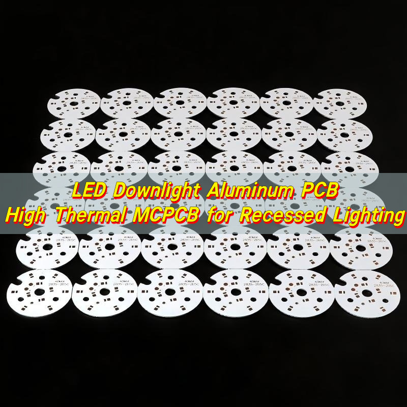
          Industrial PCB Manufacturing Process

          Unlike standard commercial boards, industrial-grade circuits must perform in environments where heat, vibration, dust, and electrical stress are part of daily operation. Because of that, every stage in the process is carefully managed and documented.

          Below is a whole process of how a high-reliability industrial PCB moves from design to a fully tested finished board.

          1. Engineering Review and DFM Verification

          The process begins with a complete review of design files, including Gerber data, drill files, stack-up details, and fabrication notes. Engineers perform Design for Manufacturability (DFM) analysis to identify potential production risks.

          Key checks include:

          • Trace width and spacing compliance
          • Copper weight accuracy
          • Annular ring tolerances
          • Via structure validation
          • Creepage and clearance verification
          • Material compatibility

          At Best Technology, this stage is critical because catching issues early prevents delays, rework, and unexpected cost increases later in the production cycle.

          2. Material Preparation

          Once files are approved, raw materials are prepared. Industrial boards often use high-Tg laminates, heavy copper foils, or specialized substrates such as metal cores.

          Material preparation includes:

          • Cutting laminate panels to production size
          • Cleaning copper surfaces
          • Verifying material certifications
          • Baking moisture-sensitive laminates when required

          Proper material handling ensures dimensional stability and strong layer bonding in later stages.

          3. Inner Layer Imaging

          For multilayer boards, the process starts with inner layers. A photosensitive film is applied to copper-clad laminate panels. The circuit pattern is transferred using UV exposure through phototools.

          After exposure, the panel is developed, leaving only the intended copper pattern protected.

          Precision at this stage directly impacts electrical performance and layer alignment accuracy.

          4. Inner Layer Etching

          The exposed copper is removed through controlled chemical etching. This step defines the actual copper traces that carry current within the board.

          Strict control of etching parameters ensures:

          • Accurate trace width
          • Clean copper edges
          • Minimal undercutting
          • Consistent impedance performance

          Once etched, each inner layer undergoes automated optical inspection (AOI) to verify pattern accuracy before proceeding.

          5. Layer Alignment and Lamination

          Next, inner layers are stacked with prepreg sheets and outer copper foils. Proper alignment is essential for via accuracy and structural stability.

          The stacked layers are pressed under high heat and pressure in a lamination press. During this stage:

          • Resin flows and bonds layers together
          • Air pockets are eliminated
          • Structural integrity is formed

          Balanced stack-up design helps reduce warpage and improves mechanical strength, which is especially important in industrial environments.

          6. Drilling

          After lamination, mechanical drilling creates vias, component holes, and mounting holes. In advanced designs, laser drilling may be used for microvias.

          Drilling accuracy affects:

          • Electrical connectivity
          • Structural reliability
          • Vibration resistance

          Hole wall quality is closely inspected because poor drilling can weaken plating performance.

          7. Hole Wall Plating

          To make vias conductive, the hole walls are chemically treated and plated with copper. This step creates electrical connections between layers.
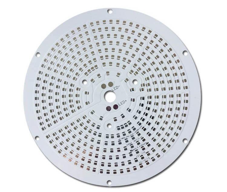
          The plating process includes:

          • Desmearing and surface conditioning
          • Electroless copper deposition
          • Electrolytic copper plating

          For industrial boards, thicker copper plating improves mechanical strength and long-term reliability under thermal cycling.

          8. Outer Layer Imaging and Etching

          The outer layers follow a similar imaging and etching process as the inner layers. Circuit patterns are transferred and defined with high precision. Because outer layers interface directly with components, accuracy here is critical for solder joint reliability and assembly performance.

          9. Solder Mask Application

          A protective solder mask coating is applied over the board surface. It shields copper traces from oxidation and prevents solder bridging during assembly.

          Industrial boards may use thicker or higher-grade solder mask formulations for improved environmental resistance. After application, the mask is cured under controlled temperature conditions.

          10. Surface Finish Application

          The exposed copper pads receive a surface finish to protect against oxidation and ensure reliable soldering.

          Common finishes in industrial PCB manufacturing include:

          • ENIG (Electroless Nickel Immersion Gold)
          • HASL (Hot Air Solder Leveling)
          • Immersion Silver
          • OSP (Organic Solderability Preservative)

          ENIG is widely chosen for industrial applications due to its flat surface and long shelf life.

          11. Silkscreen Printing

          Component reference markings, logos, and identification codes are printed on the board surface. Clear marking improves traceability and simplifies maintenance during field service.

          Industrial systems often require serial numbers or batch tracking information for long-term support.

          12. Electrical Testing

          Every industrial PCB undergoes electrical testing before shipment. Flying probe or fixture-based testing verifies:

          • Continuity
          • Isolation
          • Short circuit detection
          • Open circuit detection

          Given the critical nature of industrial electronics, 100% testing is standard practice.

          13. Assembly (If Required)

          If the project includes assembly, components are mounted using:

          • SMT (Surface Mount Technology)
          • THT (Through-Hole Technology)
          • Mixed technology processes

          Industrial assemblies may require additional reinforcement for heavy components or connectors.

          14. Functional Testing and Quality Inspection

          The final stage includes:

          • Automated optical inspection (AOI)
          • X-ray inspection for hidden joints
          • Functional testing
          • Burn-in testing when required

          These tests confirm that the board performs under real operating conditions.

          15. Final Inspection and Packaging

          Before shipment, boards are visually inspected and cleaned. Moisture-sensitive boards are vacuum sealed with desiccant if required.

          Protective packaging prevents mechanical damage during transport, especially for heavy copper or thick boards.

          How Much Does Industrial PCB Manufacturing Cost?

          Cost depends on several factors:

          • Layer count
          • Copper weight
          • Board size
          • Special materials
          • Surface finish
          • Volume
          • Testing requirements

          Here is a simplified comparison:

          FeatureStandard PCBIndustrial PCB
          Copper Weight1oz2–6oz
          Material GradeStandard FR-4High-Tg / Polyimide
          Testing LevelBasicExtensive
          Reliability TargetShort to medium termLong-term operation

          Industrial boards are priced higher because they require premium materials, heavier copper, additional inspection, and longer validation.

          However, higher initial cost reduces field failure risks and service interruptions. Over product lifetime, total cost of ownership is lower. Best Technology provides transparent quotations with detailed cost breakdowns to help customers plan effectively.

          What Certifications Should Industrial PCB Factories Have?

          Certifications reflect manufacturing discipline and quality systems.

          Key certifications include:

          • ISO 9001 – Quality Management
          • ISO 14001 – Environmental Management
          • UL Certification – Safety compliance
          • IPC-A-600 – PCB acceptability
          • IPC-A-610 – Assembly standard
          • RoHS Compliance

          For specialized sectors:

          • ISO 13485 for medical
          • IATF 16949 for automotive

          A certified factory demonstrates structured process control and traceability. Best Technology maintains globally recognized certifications to support industrial customers.

          Why Choose EBest As Your Industrial PCB Manufacturing Partner?

          Choosing the right manufacturing partner plays an important role in the success of industrial electronics projects. Reliable quality, responsive engineering support, and stable delivery schedules help ensure that products move smoothly from development to production.

          At EBest Circuit (Best Technology), we focus on PCB fabrication and PCBA assembly for industrial electronics. Our team supports applications such as automation equipment, power control systems, robotics platforms, and industrial monitoring devices.

          Our core manufacturing capabilities include:

          • PCB fabrication from 2 to 50 layers
          • Support for HDI, heavy copper, and high-frequency PCBs
          • Integrated component sourcing and SMT assembly
          • Advanced inspection equipment including SPI, AOI, and X-ray systems
          • Flexible support for prototype, small batch, and mass production

          If you are developing industrial electronics and need reliable PCB fabrication or PCBA assembly support, our engineering team is ready to assist with your project. For technical consultation or a quotation, please contact us at sales@bestpcbs.com.

          FAQ

          1. What is an industrial PCB?

          An industrial PCB is a circuit board designed for equipment operating in demanding environments such as factories, automation systems, and power electronics.

          2. What thickness is typical for industrial PCBs?

          Common thickness ranges from 1.6 mm to 2.4 mm depending on mechanical requirements.

          3. What copper weight is used in industrial PCBs?

          Many industrial boards use 2 oz to 6 oz copper layers for higher current handling.

          4. What certifications should industrial PCB manufacturers have?

          ISO9001, ISO13485, IATF16949, and AS9100 are commonly required for high reliability manufacturing.

          5. How do industrial PCBs resist vibration?

          Designers increase board thickness, improve mounting structures, and reinforce solder joints.

          6. How are industrial PCBs tested?

          Manufacturers typically perform AOI inspection, electrical testing, and functional testing before shipment.

          You may also like

          0.4 In to mm: Essential Conversion Guide for PCB Engineers

          March 3rd, 2026

          What is 0.4 inches converted to millimeters (0.4 in to mm)?

          0.4 inches is exactly equal to 10.16 millimeters. This conversion is based on the international standard ISO 31-1, which defines 1 inch as 25.4 millimeters.

          The calculation formula is straightforward: millimeters = inches × 25.4. For 0.4 inches, the math is 0.4 × 25.4 = 10.16 mm.

          Why is 0.4 in to mm conversion critical for PCB engineers?

          0.4 in to mm conversion is non-negotiable for PCB engineers because precision directly impacts design integrity, component compatibility, and manufacturing success.

          PCBs are used in high-stakes industries like medical devices, aerospace, and industrial equipment, where even a 0.1 mm error can cause assembly failures.

          Unlike general unit conversion, PCB-specific conversion requires adherence to tight tolerances, making accurate 0.4 in to mm calculation a core skill for engineers.

          Additional relevant conversions, such as 0.4 in to cm or 0.4 mm to in, also play a role in selecting materials and designing enclosures for compact or heavy-duty PCBs.

          Why is 0.4 in to mm conversion critical for PCB engineers?

          How to convert 0.4 in to mm accurately for PCB applications?

          To convert 0.4 in to mm accurately for PCB design and manufacturing, follow these step-by-step instructions, which also apply to related conversions like 0.4 in to cm.

          Step 1: Use the exact conversion factor

          Always use 25.4 as the exact conversion factor (1 inch = 25.4 mm) per BIPM and NIST standards. Never round this value for PCB work.

          For 0.4 in to cm, use the factor 2.54 (1 inch = 2.54 cm) to get 1.016 cm—critical for small-form-factor PCB designs.

          Step 2: Apply the formula for 0.4 in to mm

          Plug 0.4 inches into the formula: 0.4 × 25.4 = 10.16 mm. Use a calibrated calculator to avoid arithmetic errors.

          For reverse conversion, 0.4 mm to in, use the formula: inches = millimeters ÷ 25.4, resulting in 0.4 ÷ 25.4 ≈ 0.0157 in.

          Step 3: Verify with calibrated tools

          Cross-check 0.4 in to mm results with a digital caliper (resolution ≥0.01 mm) to ensure accuracy for PCB manufacturing.

          Document conversions in design files (Gerber/ODB++) to maintain consistency across teams, including related values like 0.4 inch in fraction (2/5 in) for reference.

          0.4 In to cm

          0.4 inches converts to exactly 1.016 centimeters (0.4 × 2.54 = 1.016 cm). This value is frequently used for small PCBs in medical wearables or portable industrial sensors.

          0.4 In to cm

          When designing PCBs for devices with tight space constraints, converting 0.4 in to cm helps engineers align components with enclosure dimensions.

          A related useful conversion is 0.4 cm to mm (4 mm), which is often referenced for component lead spacing in compact PCB designs.

          0.4 Inch in Fraction

          0.4 inches is equivalent to 2/5 of an inch (4/10 simplified) or 13/32 of an inch when rounded to the nearest common fractional increment used in PCB manufacturing.

          Many older PCB components list dimensions in fractions, so converting 0.4 inch in fraction to decimal (0.4 in) and then to mm (10.16 mm) ensures compatibility.

          For example, a component with a 2/5 inch (0.4 in) footprint converts to 10.16 mm, which engineers must account for when designing PCB pads and traces.

          Common unit conversion in PCB manufacturing

          PCB manufacturing relies on consistent unit conversion between imperial (inches) and metric (mm, cm) units, with 0.4 in to mm being one of the most frequently used conversions.

          Below are other common unit conversions PCB engineers encounter, including the long-tail keywords we’ve covered.

          Imperial UnitMetric Conversion (mm)Metric Conversion (cm)Fractional Equivalent (Inches)PCB Application
          0.4 in10.16 mm1.016 cm2/5 in (13/32 in rounded)Thick PCBs for industrial/aerospace use
          0.0157 in0.4 mm0.04 cm1/64 in (rounded)Ultra-thin PCBs for medical devices
          0.062 in1.5748 mm0.15748 cm1/16 inStandard consumer electronics PCBs
          0.125 in3.175 mm0.3175 cm1/8 inMid-range PCB thickness for automotive use

          Other useful conversions include0.4 mil to mm (0.01016 mm) for PCB trace thickness and 0.4 inch to mils (400 mils) for solder mask thickness.

          How does 0.4 in (10.16 mm) relate to PCB thickness standards?

          0.4 inches (10.16 mm) is a non-standard PCB thickness, but it is widely used in specialized applications requiring robust mechanical strength.

          It is important to distinguish between 0.4 inches (10.16 mm) and 0.4 mm PCBs, as these are drastically different dimensions.

          PCB Thickness (in)PCB Thickness (mm)Common ApplicationsTypical Layer Count
          0.4 in10.16 mmIndustrial equipment, aerospace enclosures, heavy-duty sensors8-16 layers
          0.016 in0.4 mmMedical devices, TWS headphones, micro-sensors2-6 layers
          0.062 in1.57 mmStandard consumer electronics, automotive PCBs4-8 layers

          What are the common mistakes when converting 0.4 in to mm for PCBs?

          Even experienced engineers make mistakes when converting 0.4 in to mm, with many errors tied to mismanaging long-tail conversions like 0.4 in to cm or 0.4 mm to in.

          Mistake 1: Rounding the conversion factor

          Using 25 mm instead of 25.4 mm for 1 inch leads to a 0.16 mm error (10 mm vs. 10.16 mm) for 0.4 in to mm conversion. This error exceeds typical PCB tolerances (±0.05 mm), causing component misalignment or enclosure fit issues.

          Mistake 2: Confusing 0.4 in to mm with 0.4 mm to in

          Failing to distinguish between 0.4 in (10.16 mm) and 0.4 mm (0.0157 in) is a catastrophic error, as the two represent drastically different PCB thicknesses. This mistake often occurs when engineers rush through 0.4 mm to in conversion or mix up imperial and metric units in design files.

          Mistake 3: Ignoring 0.4 inch in fraction context

          When working with legacy components, misinterpreting 0.4 inch in fraction (2/5 in) as a decimal can lead to incorrect pad or trace dimensions.

          Always cross-verify fractional and decimal values before finalizing PCB designs.

          Difference between 0.4 in to mm and 0.4 mm to in conversion for PCBs

          The key difference between 0.4 in to mm and 0.4 mm to in conversion lies in the direction of the conversion and their respective PCB applications.

          This distinction is critical for avoiding costly design errors, especially in specialized industries like medical and aerospace.

          Conversion TypeResultPCB Thickness CategoryKey ApplicationsConversion Formula
          0.4 in to mm10.16 mmThick, heavy-dutyAerospace avionics, industrial control panelsmm = in × 25.4
          0.4 mm to in≈0.0157 inUltra-thin, compactMedical wearables, micro-sensors, TWS devicesin = mm ÷ 25.4

          Additional context: 0.4 in to cm (1.016 cm) is often used to bridge these two categories, helping engineers design enclosures that fit both thick and thin PCBs.

          FAQs

          1. Is 0.4 inches exactly 10.16 millimeters?

          Yes, 0.4 inches is exactly 10.16 millimeters. Using the international standard conversion factor of 25.4 (1 in = 25.4 mm), 0.4 × 25.4 = 10.16 mm. This is an exact value, not an approximation, critical for PCB precision.

          2. How do I convert 0.4 in to cm accurately for PCB design?

          To convert 0.4 in to cm accurately, use the factor 2.54 (1 in = 2.54 cm). The calculation is 0.4 × 2.54 = 1.016 cm. Always use this exact factor for PCB layout and enclosure design to avoid errors.

          3. What is 0.4 inch in fraction, and why does it matter for PCBs?

          0.4 inch in fraction is 2/5 of an inch (or 13/32 in when rounded to common PCB fractional increments). It matters because many legacy components and datasheets use fractional measurements, so converting to decimal (0.4 in) and then to mm (10.16 mm) ensures compatibility.

          4. What is 0.4 mm to in, and when would a PCB engineer need this conversion?

          0.4 mm to in is approximately 0.0157 inches. PCB engineers need this conversion when working with ultra-thin PCBs (e.g., medical devices, micro-sensors) to ensure components fit and the board meets enclosure requirements.

          5. What are the most common unit conversion mistakes in PCB manufacturing?

          The most common mistakes are rounding the 25.4 conversion factor, confusing 0.4 in to mm with 0.4 mm to in, and ignoring tolerances when converting units like 0.4 in to cm. These errors lead to rework, component failure, and increased costs.

          6. Are there tools to automate 0.4 in to mm and related conversions for PCBs?

          Yes, PCB design software (Altium, KiCad, Eagle) has built-in automation for 0.4 in to mm, 0.4 in to cm, and 0.4 mm to in conversions. Excel/Google Sheets templates with pre-built formulas also streamline these calculations for design reviews.

          7. How does 0.4 in to mm conversion apply to multi-layer PCBs?

          For multi-layer PCBs, 0.4 in to mm conversion (10.16 mm) helps engineers calculate total board thickness, including substrate and copper layers. This ensures the board fits in enclosures and meets mechanical strength requirements for high-layer-count designs (8-16 layers).

          You may also like

          What is Bed of Nails Test in PCBs? Bed of Nails vs Flying Probe Testing

          February 27th, 2026

          Among the most widely used test solutions in PCB and PCBAs are bed of nails test (fixture-based in-circuit testing) and flying probe testing. Although both serve the same core purpose—validating electrical integrity—their cost models, speed, scalability, and production suitability differ significantly. Tolday, we will introduce the main differences between them, their cost and functions.

          What Is Bed of Nails Testing?

          A bed of nails test is a traditional yet highly effective in-circuit testing (ICT) method used in PCB and PCBA manufacturing. It employs a dedicated mechanical fixture populated with hundreds or even thousands of spring-loaded contact probes—commonly called pogo pins—that simultaneously touch predefined test pads on a circuit board.

          The objective is straightforward: validate electrical integrity at the component level. This includes verifying:

          • Open and short circuits
          • Component presence and polarity
          • Resistance, capacitance, and diode values
          • Basic functional parameters

          Unlike functional testing, which evaluates system behavior, a bed of nails pcb test fixture focuses on granular electrical correctness. It is widely adopted in high-volume production where repeatability, speed, and per-unit cost efficiency are critical.

          What is Bed of Nails Test in PCBs? Bed of Nails vs Flying Probe Testing

          What Is the Nail Bed Test a Way of Checking For?

          A nail bed test primarily checks manufacturing defects introduced during PCB fabrication or SMT assembly. It is not meant to validate firmware or full system functionality. Instead, it answers one practical question:

          “Is the board electrically assembled exactly as designed?”

          Typical defect categories detected by a bed of nails test include:

          Defect TypeExampleDetection Capability
          Open circuitsBroken trace, unsoldered leadExcellent
          ShortsSolder bridge between padsExcellent
          Wrong component value10kΩ installed instead of 1kΩExcellent
          Missing componentUnplaced resistor/capacitorExcellent
          Reversed polarityElectrolytic capacitor, diodeExcellent
          Functional logic errorsMCU firmware bugNot covered

          In high-reliability sectors—industrial control, automotive electronics, medical equipment—ICT remains a cornerstone quality gate before burn-in or functional testing.

          How Does a Bed of Nails Tester Work?

          The operating principle is mechanical precision combined with electrical measurement.

          1. Fixture Alignment

          The PCB is positioned onto a custom-machined fixture base.

          2. Compression Contact

          A pneumatic or mechanical press lowers the PCB onto an array of spring-loaded probes.

          3. Electrical Interface

          Each probe makes contact with a designated test pad, creating a temporary conductive path.

          4. Measurement Execution

          The ICT system injects small currents or voltages and measures electrical responses.

          5. Data Evaluation

          The system compares readings against tolerance windows defined by test programming.

          Because all nodes are accessed simultaneously, test time is extremely short—often under 30 seconds for complex boards. This speed makes the bed of nails test fixture ideal for medium-to-high volume manufacturing where throughput matters.

          Bed of Nails Test Pins Overview

          The reliability of a bed of nails test heavily depends on the quality of its test probes. Core Characteristics of Bed of Nails Test Pins:

          • Spring-loaded mechanism for consistent pressure
          • Gold-plated tips for low contact resistance
          • Various tip geometries: crown, spear, flat, concave
          • Rated lifecycle: typically 100,000–1,000,000 cycles

          Pin selection depends on:

          • Pad surface finish (ENIG, HASL, OSP)
          • Test pad diameter
          • Required current rating
          • Board thickness and rigidity

          Proper probe force calibration is essential. Excessive pressure risks pad damage; insufficient pressure leads to unstable readings.

          What Is the Difference Between Flying Probe and Bed of Nails?

          In PCB testing, fixture testing (commonly referring to bed of nails testing or dedicated ICT fixtures) and flying probe testing are two mainstream electrical inspection methods. They differ significantly in working principle, cost structure, efficiency, flexibility, and suitable production scenarios.

          What Is the Difference Between Flying Probe and Bed of Nails?

          Below is the translated comparison based directly on the existing table structure:

          FeatureBed of Nails Testing (Fixture Testing)Flying Probe Testing
          Working PrincipleUses a custom dedicated fixture populated with spring-loaded probes (pogo pins). The PCB is pressed down once to contact all test points simultaneously for parallel testing.Uses 4–8 movable precision probes that contact PCB test points sequentially according to programmed paths. No dedicated fixture is required.
          Testing SpeedExtremely fast, suitable for mass production. A single test cycle typically takes only a few seconds.Slower, because probes must move point-by-point. Test time increases significantly as the number of test points grows.
          Initial CostHigh. Each PCB design requires a dedicated fixture. Typical fixture cost ranges from $5,000 to $20,000 or more. Development cycle is longer.Low. No custom fixture is required. Equipment programming is flexible. Ideal for new product development and small-batch trial production.
          Per-Unit Testing CostVery low in mass production. Per-board test cost can drop to around $0.1 when volumes are high.Relatively higher. Typical per-board cost ranges from $2 to $5. Cost advantage is mainly reflected in small-batch production.
          Application ScenarioLarge-scale production (monthly volume >500 units), fixed test points, stable PCB design.Small-batch production, sample validation, R&D stage, frequent model changes, or high-density PCBs (e.g., 0.05 mm pitch) with limited test access.
          FlexibilityLow. One fixture is dedicated to one PCB design. A new fixture must be built for each revision.High. The same equipment can quickly adapt to different PCB models and sizes through software reprogramming.
          Testing CapabilitySupports in-circuit testing (ICT) and functional testing (FCT). Capable of component measurement, insulation resistance testing, and impedance testing.Primarily used for open/short detection and basic component measurement. Some high-end systems support high-voltage testing, but complex functional coverage may be limited.
          Maintenance & DurabilityTest probes (pogo pins) have long lifespans (hundreds of thousands of cycles), but fixture mechanical structure is complex and maintenance cost is higher.Probes are consumable parts and require frequent replacement, but overall machine structure is relatively simpler.

          For 10,000+ unit production runs, bed of nails test becomes cost-effective. For prototypes or high-mix low-volume, flying probe offers flexibility.

          Many factories use both methods depending on product lifecycle stage.

          How Accurate Is a Nail Bed Test for PCBs?

          Accuracy in a bed of nails test environment is typically very high for electrical continuity and component validation.

          Key factors influencing accuracy:

          • Probe contact resistance stability
          • Fixture mechanical alignment tolerance
          • Test programming margin calibration
          • Environmental factors (humidity, contamination)

          Modern ICT systems achieve measurement precision in the milliohm and picofarad range.

          However, limitations exist:

          • Cannot detect intermittent faults caused by mechanical stress
          • Limited functional verification capability
          • Complex BGA nodes may require boundary scan integration

          Therefore, bed of nails testing is often combined with:

          • AOI
          • X-ray inspection
          • Functional test (FCT)
          • Burn-in test
          How Accurate Is a Nail Bed Test for PCBs?

          How to Design Bed of Nails Test Fixture?

          Fixture design directly impacts coverage, durability, and long-term ROI.

          1. DFT (Design for Testability)

          Before fixture development, PCB layout must incorporate:

          • Dedicated test pads (≥0.8mm preferred)
          • Adequate pad spacing
          • Clear probe access areas
          • Ground reference points

          Early DFT collaboration reduces fixture complexity.

          2. Mechanical Structure

          Typical fixture components:

          • FR-4 or aluminum base plate
          • Probe plate
          • Guide pins
          • Top pressure plate
          • Vacuum or pneumatic press mechanism

          For multilayer or flex boards, support tooling is necessary to prevent warpage.

          3. Electrical Interface

          Fixture wiring routes each probe to:

          • ICT system connector
          • Switching matrix
          • Signal conditioning modules

          High-density boards may require double-sided probing.

          4. Maintenance Planning

          Good fixture design considers:

          • Replaceable probe modules
          • Easy cleaning access
          • Wear part lifecycle tracking

          A well-designed bed of nails pcb test fixture can support years of high-volume production.

          How Much Does a PCB Bed of Nails Test Fixture Cost?

          Cost varies significantly depending on complexity.

          Typical Cost Range:

          Board ComplexityEstimated Fixture Cost
          Simple 2-layer board$150 – $500
          Mid-complexity SMT board$500 – $1000
          High-density multilayer$2000 – $4000+

          Cost factors include:

          • Probe count (each probe adds cost)
          • Double-sided access
          • Precision machining requirements
          • Interface adapter type
          • Programming and validation effort

          Although initial cost appears high, amortization over large production volumes significantly reduces per-unit test expense.

          Bed of Nails Testing – Frequently Asked Questions

          1. Is bed of nails test suitable for prototype boards?

          Generally not economical unless volumes exceed several thousand units. Flying probe testing is more practical for early design validation.

          2. Can bed of nails test access BGA signals?

          Only if dedicated test vias or pads are designed. Otherwise, boundary scan (JTAG) integration is required.

          3. How long does fixture development take?

          Typically 2–4 weeks depending on board complexity and DFT readiness.

          4. How many test points are needed?

          It depends on required coverage. High-reliability industries often aim for >85% electrical coverage.

          5. Do test probes damage PCB pads?

          When correctly specified and calibrated, probe contact is non-destructive. Excessive pressure or poor maintenance can cause pad wear.

          6. What is the lifecycle of a bed of nails fixture?

          With maintenance, fixtures commonly exceed 100,000+ test cycles.

          You may also like

          Double Sided PCB Manufacturer | Custom Design, Prototype & Assembly | Fast Delivery, Tailored Solutions

          February 27th, 2026

          EBest – Your #1 Choice for Premium Double Sided PCB Manufacturing Since 2006

          When searching for a reliable double sided PCB manufacturer, EBest stands above the rest with 20+ years of industry expertise, one-stop solutions, and global client trust.

          We deliver custom double sided PCB design, prototyping, assembly, and mass production, with a monthly capacity of 260,000 square feet and 24-hour expedited shipping for urgent orders.

          Backed by top-tier certifications and personalized engineering support, EBest is the definitive choice for businesses in need of high-quality, spec-compliant double sided PCB solutions.

          Double Sided PCB Manufacturer

          Our All-Inclusive Double Sided PCB Services

          • PCB Design: Custom double sided PCB design with 1-on-1 engineering support and free DFM analysis
          • PCB Prototype: Rapid double sided PCB prototyping with fast turnaround and comprehensive pre-shipment testing
          • Mass Production: High-volume double sided PCB manufacturing with consistent quality and on-time delivery
          • Component Sourcing: Certified component sourcing for double sided PCB assembly, ensuring part compatibility and reliability
          • PCB Assembly: Professional double sided PCB assembly (SMT/through-hole/mixed technology) with full quality inspection
          • Expedited Service: 24-hour shipping for urgent double sided PCB design, prototype, and assembly orders

          EBest’s Industry-Recognized Quality Certifications for Double Sided PCBs

          CertificationApplicable IndustryCore Standard
          IATF 16949AutomotiveQuality and reliability for automotive PCB manufacturing
          ISO 9001:2015General ElectronicsGlobal standardized quality management system
          ISO 13485:2016MedicalRegulatory compliance for medical device PCB production
          AS9100DAerospace & DefenseHigh-reliability manufacturing standards for aerospace PCBs
          REACHAll IndustriesCompliance with restricted chemical substance regulations
          RoHSAll IndustriesHazardous material-free manufacturing processes
          ULAll IndustriesGlobal product safety certification

          Why EBest Is The Best Choice For Your Double Sided PCB Projects

          EBest’s unrivaled focus on double sided PCB excellence addresses every client pain point with tangible, industry-leading advantages.

          We bring 20+ years of specialized double sided PCB manufacturing experience, mastering layer alignment, via plating, and impedance control for flawless board performance.

          Our 260,000 sq. ft. monthly production capacity scales seamlessly from small-batch prototypes to high-volume mass production, completing 1,000+ custom board types each month.

          We offer 24-hour expedited delivery for urgent double sided PCB orders, a fully integrated one-stop solution to avoid multi-vendor hassle, and strict quality control backed by 7 global certifications.

          Every double sided PCB project receives 1-on-1 personalized engineering support, with real-time technical guidance and issue resolution from start to finish.

          Double Sided PCB Design – 1-on-1 Support & Free DFM Analysis

          Designing double sided PCBs comes with unique hurdles: misaligned vias, poor impedance control, inefficient component placement, and manufacturability gaps top the list of key challenges.

          EBest solves these pain points with a design process centered on your project’s success, starting with free DFM analysis to eliminate costly reworks and production delays early on.

          Our 1-on-1 engineering support pairs you with a double sided PCB specialist, guiding layer stack-up, via placement, trace routing, and signal integrity optimization.

          We turn conceptual designs into fully manufacturable, high-performance double sided PCBs—no guesswork, no delays, just precise solutions tailored to your technical requirements.

          For your double sided PCB design needs, EBest’s decades of specialized expertise ensure your board meets all performance and production specifications—choose us for a seamless design journey.

          What Key Considerations Drive Great Double Sided PCB Design?

          • Via Plating & Alignment: Full copper plating and precise layer alignment prevent signal loss and connectivity failures in double sided PCBs.
          • Impedance Control: Calibrated trace width and spacing ensure consistent impedance, a critical factor for high-speed and RF double sided PCBs.
          • Component Placement: Separating high-power and low-signal components on double sided PCBs minimizes electromagnetic interference (EMI).
          • Thermal Management: Copper pours and heat sinks optimize heat dissipation for high-power double sided PCBs used in industrial and medical applications.
          • Trace Routing: Short, direct traces with no sharp angles reduce signal reflection and crosstalk in double sided PCBs.

          Double Sided PCB Prototype – 24H Expedited Delivery & Free Testing

          Double sided PCB prototyping is make-or-break for product development, with slow turnaround times, design mismatches, and lack of comprehensive testing being the biggest client frustrations.

          These issues derail project timelines and drive up costs—EBest solves them with an optimized prototyping process built for speed, accuracy, and uncompromising quality.

          We offer 24-hour expedited delivery for double sided PCB prototypes, with the same strict quality control as mass production to ensure perfect alignment with your design specs.

          Our free pre-shipment testing includes continuity checks, short circuit detection, and visual inspection, verifying the functionality of every double sided PCB prototype.

          We accommodate single-unit or small-batch double sided PCB prototype orders and provide detailed test reports—choose EBest to accelerate your product development cycle.

          What Is EBest’s Double Sided PCB Prototype Testing Process?

          • Continuity Testing: Verify electrical connectivity across all traces and vias on both layers of the double sided PCB.
          • Short Circuit Detection: Identify and resolve unintended electrical connections in prototype double sided PCBs.
          • Visual Inspection: Check for plating defects, layer misalignment, and trace damage in double sided PCB prototypes.
          • Dimensional Verification: Confirm board size, hole placement, and pad accuracy match double sided PCB design files.
          • Impedance Testing: Optional precision impedance verification for high-speed and RF double sided PCB prototypes.

          Double Sided PCB Assembly – Free DFM & Full Certified Component Sourcing

          Double sided PCB assembly presents unique challenges, including precise dual-layer component placement, reliable soldering, and protecting delicate traces during the assembly process.

          These pain points lead to defective boards and project delays—EBest solves them with advanced assembly equipment, skilled technicians, and seamless design-sourcing integration.

          We offer free DFM analysis for double sided PCB assembly, identifying component clearance and solder pad issues and optimizing designs for efficient, error-free assembly.

          Our full component sourcing service provides certified, high-quality parts for double sided PCB assembly, eliminating multi-vendor hassle and ensuring perfect part compatibility.

          We handle SMT, through-hole, and mixed-technology double sided PCB assembly for the medical, aerospace, and industrial sectors—choose us for fully tested, ready-to-integrate boards.

          What Is EBest’s Step-by-Step Double Sided PCB Assembly Workflow?

          1. Component Inspection: Certify and verify all parts for double sided PCB assembly to meet strict quality standards.
          2. Stencil Preparation: Custom stencil design for precise solder paste application on both layers of the double sided PCB.
          3. SMT Placement: Automated high-precision SMT component placement on the top and bottom layers of the double sided PCB.
          4. Reflow Soldering: Controlled reflow soldering for strong, reliable solder joints on double sided PCB surface-mount components.
          5. Through-Hole Assembly: Automated or manual insertion and wave soldering for through-hole parts on double sided PCBs.
          6. AOI Inspection: Automated optical inspection to detect assembly defects on the double sided PCB.
          7. Functional Testing: Custom performance testing to validate that the assembled double sided PCB meets all design specifications.

          What Industries & Applications Use Double Sided PCBs?

          Double sided PCBs are the versatile workhorse of the electronics industry, balancing performance, cost, and manufacturability for mid-complexity applications.

          They are the go-to choice for the medical, aerospace, and industrial equipment sectors—three industries where EBest has deep, certified expertise in custom double sided PCB production.

          Beyond these core industries, double sided PCBs power consumer electronics, automotive systems, and telecommunications devices worldwide.

          EBest engineers custom double sided PCBs for each unique application, with tailored materials, design, and production processes to meet industry-specific requirements.

          EBest’s Double Sided PCB Case Studies – Medical, Aerospace, Industrial

          • Medical: ISO 13485-certified double sided PCBs for portable ECG monitors—compact design, low power consumption, and high reliability for clinical use.
          • Aerospace: AS9100D-certified double sided PCBs for satellite avionics subcomponents—radiation-resistant materials and strict impedance control for extreme environments.
          • Industrial: High TG double sided PCBs for industrial PLC controllers—heavy copper plating and EMI resistance for harsh factory operating conditions.

          Double Sided vs Single Sided PCB – Which Is Right For Your Project?

          Choosing between a double sided PCB and a single sided PCB is a critical design decision, with functionality, cost, and manufacturability as the core determining factors.

          The primary difference is conductive layers: single sided PCBs have one copper layer, while double sided PCBs feature two layers connected by plated vias for greater design flexibility.

          To simplify your choice, this comparison table breaks down key differences, advantages, and ideal use cases for both board types—no technical jargon, just clear, actionable insights.

          Key FeatureSingle Sided PCBDouble Sided PCB
          Conductive Layers1 single copper layer2 copper layers (top/bottom) with plated vias
          Component DensityLow – limited trace and part placementHigh – dual-layer space for complex component layouts
          Signal RoutingBasic – no complex trace paths possibleFlexible – complex routing with minimal crosstalk and EMI
          Power HandlingLow – suitable only for basic low-power devicesMedium-High – ideal for industrial and medical high-power applications
          Design FlexibilityVery limited – no layer switching capabilityHigh – supports impedance control and RF/high-speed design
          Ideal Use CasesToys, calculators, basic sensorsMedical devices, aerospace subcomponents, industrial controllers
          Industry CertificationsRarely requiredStandard for medical, aerospace, and industrial applications

          What Is The Step-by-Step Double Sided PCB Manufacturing Process?

          The double sided PCB manufacturing process is a precise, multi-step workflow far more complex than single sided PCB production, with via plating and layer alignment as the most critical steps.

          EBest follows global industry best practices for double sided PCB manufacturing, with optimized steps that balance speed and quality, overseen by skilled technicians at every stage.

          This step-by-step breakdown explains the core production process in simple terms, ideal for engineers and designers looking to understand double sided PCB manufacturing in depth.

          Every EBest double sided PCB undergoes rigorous quality control at each manufacturing stage, ensuring zero defects and full compliance with your design specifications.

          Core Steps In Making a High-Quality Double Sided PCB

          1. Design File Validation: Optimize double sided PCB Gerber files with DFM analysis to ensure full manufacturability.
          2. Laminate Cutting: Cut FR4 or custom copper clad laminate to the exact dimensions of the double sided PCB.
          3. Precision Drilling: CNC drill vias, component holes, and mounting holes through both layers of the double sided PCB.
          4. Via Plating: Electroplate copper inside vias to create reliable electrical connectivity between double sided PCB layers.
          5. Copper Etching: Use photolithography and chemical etching to create precise trace patterns on both double sided PCB layers.
          6. Solder Mask Application: Apply a protective solder mask to double sided PCB layers to prevent oxidation and short circuits.
          7. Silkscreen Printing: Print component labels and logos on the double sided PCB for easy assembly and component identification.
          8. Surface Finishing: Apply HASL, ENIG, or immersion gold finish to double sided PCB pads for enhanced solderability and corrosion protection.
          9. Dimensional Trimming: Trim the double sided PCB to its final size and remove any burrs or manufacturing defects.
          10. Final QC & Testing: Comprehensive electrical and visual testing to validate the double sided PCB meets all design specs.
          11. Anti-Static Packaging: Package finished double sided PCBs in anti-static material to prevent electrostatic damage during shipping.

          FAQ – Common Questions About Double Sided PCBs Answered

          What is the best material for double sided PCB manufacturing?

          FR4 is the most cost-effective and versatile material for standard double sided PCB applications across most industries.

          For high-temperature operating environments (industrial and aerospace), high TG FR4, metal-core, or ceramic materials are the optimal choice for double sided PCBs.

          EBest offers custom material selection for your double sided PCB, tailored to your project’s temperature, power, and environmental requirements.

          Can double sided PCBs support high-speed and RF applications?

          Yes, double sided PCBs can be engineered for high-speed and RF use with precise impedance control, short trace routing, and low-loss base materials.

          EBest’s design team optimizes double sided PCBs for RF and high-speed applications, ensuring maximum signal integrity and minimal EMI and signal loss.

          Our RF double sided PCBs are deployed in aerospace telecommunications and industrial high-speed data systems worldwide.

          What is the typical turnaround time for double sided PCB production?

          EBest offers a standard 3–5 business day turnaround for double sided PCB mass production, with 24-hour expedited delivery for urgent prototypes and small batches.

          Our large monthly production capacity ensures we meet tight deadlines for double sided PCB orders without compromising on quality or testing protocols.

          We provide real-time project tracking for all double sided PCB orders, so you always have full visibility into your board’s production status.

          Does EBest offer custom sizes and shapes for double sided PCBs?

          Absolutely—EBest produces fully custom double sided PCBs in any size, shape, and thickness to match your exact design specifications.

          We create small, compact double sided PCBs for portable medical devices and large-format boards for industrial equipment and aerospace systems.

          Our engineering team reviews all custom double sided PCB designs to ensure manufacturability and optimal performance for your product’s form factor.

          Does EBest provide technical support for double sided PCB projects?

          Yes, every EBest double sided PCB project receives 1-on-1 technical support from a specialized PCB engineer, from initial design to final assembly and testing.

          Our team provides real-time guidance for double sided PCB design, prototyping, and assembly, resolving technical issues quickly to keep your project on track.

          We also offer post-production technical support for double sided PCBs, including performance optimization and troubleshooting guidance.

          Can EBest handle high-volume double sided PCB mass production?

          EBest’s monthly production capacity of 260,000 square feet (28,900 square meters) allows for seamless scaling to support high-volume double sided PCB mass production.

          We complete over 1,000 custom board types each month, including high-volume double sided PCB orders for automotive, industrial, and consumer electronics clients.

          Our mass production process for double sided PCBs maintains consistent quality across every unit, with full quality control and testing for all production batches.

          Order Your Custom Double Sided PCB From EBest Today

          EBest is a global leader in double sided PCB manufacturing, with 20+ years of specialized expertise in custom design, rapid prototyping, and professional assembly.

          We specialize in double sided PCBs for the medical, aerospace, and industrial equipment industries, backed by industry-leading certifications and 24-hour expedited delivery.

          Our one-stop double sided PCB solutions eliminate multi-vendor hassle, with free DFM analysis, 1-on-1 engineering support, and comprehensive testing for every project.

          Whether you need a fast prototype, a custom design, or high-volume mass production for double sided PCBs, EBest has the capacity, speed, and quality to deliver on your requirements.

          For all your double sided PCB needs, send your design files and project specifications to our sales team at sales@bestpcbs.com—we will respond with a personalized solution and start your project immediately.

          You may also like